DE102023133275A1 - Process for producing a transparent, scratch-resistant component - Google Patents
Process for producing a transparent, scratch-resistant componentDownload PDFInfo
- Publication number
- DE102023133275A1 DE102023133275A1DE102023133275.9ADE102023133275ADE102023133275A1DE 102023133275 A1DE102023133275 A1DE 102023133275A1DE 102023133275 ADE102023133275 ADE 102023133275ADE 102023133275 A1DE102023133275 A1DE 102023133275A1
- Authority
- DE
- Germany
- Prior art keywords
- metal film
- diamond
- vapor deposition
- growth
- nickel
- Prior art date
- Legal status (The legal status is an assumption and is not a legal conclusion. Google has not performed a legal analysis and makes no representation as to the accuracy of the status listed.)
- Pending
Links
Images

Classifications
- C—CHEMISTRY; METALLURGY
- C23—COATING METALLIC MATERIAL; COATING MATERIAL WITH METALLIC MATERIAL; CHEMICAL SURFACE TREATMENT; DIFFUSION TREATMENT OF METALLIC MATERIAL; COATING BY VACUUM EVAPORATION, BY SPUTTERING, BY ION IMPLANTATION OR BY CHEMICAL VAPOUR DEPOSITION, IN GENERAL; INHIBITING CORROSION OF METALLIC MATERIAL OR INCRUSTATION IN GENERAL
- C23C—COATING METALLIC MATERIAL; COATING MATERIAL WITH METALLIC MATERIAL; SURFACE TREATMENT OF METALLIC MATERIAL BY DIFFUSION INTO THE SURFACE, BY CHEMICAL CONVERSION OR SUBSTITUTION; COATING BY VACUUM EVAPORATION, BY SPUTTERING, BY ION IMPLANTATION OR BY CHEMICAL VAPOUR DEPOSITION, IN GENERAL
- C23C16/00—Chemical coating by decomposition of gaseous compounds, without leaving reaction products of surface material in the coating, i.e. chemical vapour deposition [CVD] processes
- C23C16/02—Pretreatment of the material to be coated
- C23C16/0272—Deposition of sub-layers, e.g. to promote the adhesion of the main coating
- C23C16/0281—Deposition of sub-layers, e.g. to promote the adhesion of the main coating of metallic sub-layers
- C—CHEMISTRY; METALLURGY
- C23—COATING METALLIC MATERIAL; COATING MATERIAL WITH METALLIC MATERIAL; CHEMICAL SURFACE TREATMENT; DIFFUSION TREATMENT OF METALLIC MATERIAL; COATING BY VACUUM EVAPORATION, BY SPUTTERING, BY ION IMPLANTATION OR BY CHEMICAL VAPOUR DEPOSITION, IN GENERAL; INHIBITING CORROSION OF METALLIC MATERIAL OR INCRUSTATION IN GENERAL
- C23C—COATING METALLIC MATERIAL; COATING MATERIAL WITH METALLIC MATERIAL; SURFACE TREATMENT OF METALLIC MATERIAL BY DIFFUSION INTO THE SURFACE, BY CHEMICAL CONVERSION OR SUBSTITUTION; COATING BY VACUUM EVAPORATION, BY SPUTTERING, BY ION IMPLANTATION OR BY CHEMICAL VAPOUR DEPOSITION, IN GENERAL
- C23C16/00—Chemical coating by decomposition of gaseous compounds, without leaving reaction products of surface material in the coating, i.e. chemical vapour deposition [CVD] processes
- C23C16/006—Chemical coating by decomposition of gaseous compounds, without leaving reaction products of surface material in the coating, i.e. chemical vapour deposition [CVD] processes characterized by the colour of the layer
- C—CHEMISTRY; METALLURGY
- C23—COATING METALLIC MATERIAL; COATING MATERIAL WITH METALLIC MATERIAL; CHEMICAL SURFACE TREATMENT; DIFFUSION TREATMENT OF METALLIC MATERIAL; COATING BY VACUUM EVAPORATION, BY SPUTTERING, BY ION IMPLANTATION OR BY CHEMICAL VAPOUR DEPOSITION, IN GENERAL; INHIBITING CORROSION OF METALLIC MATERIAL OR INCRUSTATION IN GENERAL
- C23C—COATING METALLIC MATERIAL; COATING MATERIAL WITH METALLIC MATERIAL; SURFACE TREATMENT OF METALLIC MATERIAL BY DIFFUSION INTO THE SURFACE, BY CHEMICAL CONVERSION OR SUBSTITUTION; COATING BY VACUUM EVAPORATION, BY SPUTTERING, BY ION IMPLANTATION OR BY CHEMICAL VAPOUR DEPOSITION, IN GENERAL
- C23C16/00—Chemical coating by decomposition of gaseous compounds, without leaving reaction products of surface material in the coating, i.e. chemical vapour deposition [CVD] processes
- C23C16/01—Chemical coating by decomposition of gaseous compounds, without leaving reaction products of surface material in the coating, i.e. chemical vapour deposition [CVD] processes on temporary substrates, e.g. substrates subsequently removed by etching
- C—CHEMISTRY; METALLURGY
- C23—COATING METALLIC MATERIAL; COATING MATERIAL WITH METALLIC MATERIAL; CHEMICAL SURFACE TREATMENT; DIFFUSION TREATMENT OF METALLIC MATERIAL; COATING BY VACUUM EVAPORATION, BY SPUTTERING, BY ION IMPLANTATION OR BY CHEMICAL VAPOUR DEPOSITION, IN GENERAL; INHIBITING CORROSION OF METALLIC MATERIAL OR INCRUSTATION IN GENERAL
- C23C—COATING METALLIC MATERIAL; COATING MATERIAL WITH METALLIC MATERIAL; SURFACE TREATMENT OF METALLIC MATERIAL BY DIFFUSION INTO THE SURFACE, BY CHEMICAL CONVERSION OR SUBSTITUTION; COATING BY VACUUM EVAPORATION, BY SPUTTERING, BY ION IMPLANTATION OR BY CHEMICAL VAPOUR DEPOSITION, IN GENERAL
- C23C16/00—Chemical coating by decomposition of gaseous compounds, without leaving reaction products of surface material in the coating, i.e. chemical vapour deposition [CVD] processes
- C23C16/02—Pretreatment of the material to be coated
- C23C16/0209—Pretreatment of the material to be coated by heating
- C—CHEMISTRY; METALLURGY
- C23—COATING METALLIC MATERIAL; COATING MATERIAL WITH METALLIC MATERIAL; CHEMICAL SURFACE TREATMENT; DIFFUSION TREATMENT OF METALLIC MATERIAL; COATING BY VACUUM EVAPORATION, BY SPUTTERING, BY ION IMPLANTATION OR BY CHEMICAL VAPOUR DEPOSITION, IN GENERAL; INHIBITING CORROSION OF METALLIC MATERIAL OR INCRUSTATION IN GENERAL
- C23C—COATING METALLIC MATERIAL; COATING MATERIAL WITH METALLIC MATERIAL; SURFACE TREATMENT OF METALLIC MATERIAL BY DIFFUSION INTO THE SURFACE, BY CHEMICAL CONVERSION OR SUBSTITUTION; COATING BY VACUUM EVAPORATION, BY SPUTTERING, BY ION IMPLANTATION OR BY CHEMICAL VAPOUR DEPOSITION, IN GENERAL
- C23C16/00—Chemical coating by decomposition of gaseous compounds, without leaving reaction products of surface material in the coating, i.e. chemical vapour deposition [CVD] processes
- C23C16/22—Chemical coating by decomposition of gaseous compounds, without leaving reaction products of surface material in the coating, i.e. chemical vapour deposition [CVD] processes characterised by the deposition of inorganic material, other than metallic material
- C23C16/26—Deposition of carbon only
- C23C16/27—Diamond only
- C23C16/271—Diamond only using hot filaments
- C—CHEMISTRY; METALLURGY
- C23—COATING METALLIC MATERIAL; COATING MATERIAL WITH METALLIC MATERIAL; CHEMICAL SURFACE TREATMENT; DIFFUSION TREATMENT OF METALLIC MATERIAL; COATING BY VACUUM EVAPORATION, BY SPUTTERING, BY ION IMPLANTATION OR BY CHEMICAL VAPOUR DEPOSITION, IN GENERAL; INHIBITING CORROSION OF METALLIC MATERIAL OR INCRUSTATION IN GENERAL
- C23C—COATING METALLIC MATERIAL; COATING MATERIAL WITH METALLIC MATERIAL; SURFACE TREATMENT OF METALLIC MATERIAL BY DIFFUSION INTO THE SURFACE, BY CHEMICAL CONVERSION OR SUBSTITUTION; COATING BY VACUUM EVAPORATION, BY SPUTTERING, BY ION IMPLANTATION OR BY CHEMICAL VAPOUR DEPOSITION, IN GENERAL
- C23C16/00—Chemical coating by decomposition of gaseous compounds, without leaving reaction products of surface material in the coating, i.e. chemical vapour deposition [CVD] processes
- C23C16/22—Chemical coating by decomposition of gaseous compounds, without leaving reaction products of surface material in the coating, i.e. chemical vapour deposition [CVD] processes characterised by the deposition of inorganic material, other than metallic material
- C23C16/26—Deposition of carbon only
- C23C16/27—Diamond only
- C23C16/274—Diamond only using microwave discharges
- C—CHEMISTRY; METALLURGY
- C23—COATING METALLIC MATERIAL; COATING MATERIAL WITH METALLIC MATERIAL; CHEMICAL SURFACE TREATMENT; DIFFUSION TREATMENT OF METALLIC MATERIAL; COATING BY VACUUM EVAPORATION, BY SPUTTERING, BY ION IMPLANTATION OR BY CHEMICAL VAPOUR DEPOSITION, IN GENERAL; INHIBITING CORROSION OF METALLIC MATERIAL OR INCRUSTATION IN GENERAL
- C23C—COATING METALLIC MATERIAL; COATING MATERIAL WITH METALLIC MATERIAL; SURFACE TREATMENT OF METALLIC MATERIAL BY DIFFUSION INTO THE SURFACE, BY CHEMICAL CONVERSION OR SUBSTITUTION; COATING BY VACUUM EVAPORATION, BY SPUTTERING, BY ION IMPLANTATION OR BY CHEMICAL VAPOUR DEPOSITION, IN GENERAL
- C23C16/00—Chemical coating by decomposition of gaseous compounds, without leaving reaction products of surface material in the coating, i.e. chemical vapour deposition [CVD] processes
- C23C16/22—Chemical coating by decomposition of gaseous compounds, without leaving reaction products of surface material in the coating, i.e. chemical vapour deposition [CVD] processes characterised by the deposition of inorganic material, other than metallic material
- C23C16/26—Deposition of carbon only
- C23C16/27—Diamond only
- C23C16/279—Diamond only control of diamond crystallography
- C—CHEMISTRY; METALLURGY
- C30—CRYSTAL GROWTH
- C30B—SINGLE-CRYSTAL GROWTH; UNIDIRECTIONAL SOLIDIFICATION OF EUTECTIC MATERIAL OR UNIDIRECTIONAL DEMIXING OF EUTECTOID MATERIAL; REFINING BY ZONE-MELTING OF MATERIAL; PRODUCTION OF A HOMOGENEOUS POLYCRYSTALLINE MATERIAL WITH DEFINED STRUCTURE; SINGLE CRYSTALS OR HOMOGENEOUS POLYCRYSTALLINE MATERIAL WITH DEFINED STRUCTURE; AFTER-TREATMENT OF SINGLE CRYSTALS OR A HOMOGENEOUS POLYCRYSTALLINE MATERIAL WITH DEFINED STRUCTURE; APPARATUS THEREFOR
- C30B25/00—Single-crystal growth by chemical reaction of reactive gases, e.g. chemical vapour-deposition growth
- C30B25/02—Epitaxial-layer growth
- C30B25/18—Epitaxial-layer growth characterised by the substrate
- C30B25/183—Epitaxial-layer growth characterised by the substrate being provided with a buffer layer, e.g. a lattice matching layer
- C—CHEMISTRY; METALLURGY
- C30—CRYSTAL GROWTH
- C30B—SINGLE-CRYSTAL GROWTH; UNIDIRECTIONAL SOLIDIFICATION OF EUTECTIC MATERIAL OR UNIDIRECTIONAL DEMIXING OF EUTECTOID MATERIAL; REFINING BY ZONE-MELTING OF MATERIAL; PRODUCTION OF A HOMOGENEOUS POLYCRYSTALLINE MATERIAL WITH DEFINED STRUCTURE; SINGLE CRYSTALS OR HOMOGENEOUS POLYCRYSTALLINE MATERIAL WITH DEFINED STRUCTURE; AFTER-TREATMENT OF SINGLE CRYSTALS OR A HOMOGENEOUS POLYCRYSTALLINE MATERIAL WITH DEFINED STRUCTURE; APPARATUS THEREFOR
- C30B29/00—Single crystals or homogeneous polycrystalline material with defined structure characterised by the material or by their shape
- C30B29/02—Elements
- C30B29/04—Diamond
Landscapes
- Chemical & Material Sciences (AREA)
- Engineering & Computer Science (AREA)
- Materials Engineering (AREA)
- Metallurgy (AREA)
- Organic Chemistry (AREA)
- Chemical Kinetics & Catalysis (AREA)
- General Chemical & Material Sciences (AREA)
- Mechanical Engineering (AREA)
- Crystallography & Structural Chemistry (AREA)
- Inorganic Chemistry (AREA)
- Crystals, And After-Treatments Of Crystals (AREA)
- Chemical Vapour Deposition (AREA)
Abstract
Translated fromGermanDescription
Translated fromGermanDie Erfindung betrifft ein Verfahren zur Herstellung eines durchsichtigen, kratzfesten Bauteils (Ausführungsvariante 1) sowie ein Verfahren zur Herstellung einer Diamantscheibe (Ausführungsvariante 2).The invention relates to a method for producing a transparent, scratch-resistant component (embodiment variant 1) and a method for producing a diamond disc (embodiment variant 2).
Es ist Aufgabe der Erfindung, Verfahren anzugeben, die die effiziente Herstellung eines durchsichtigen, kratzfesten Bauteils sowie einer Diamantscheibe ermöglichen.The object of the invention is to provide methods which enable the efficient production of a transparent, scratch-resistant component and a diamond disc.
Die Lösung dieser Aufgabe erfolgt durch die Merkmale der unabhängigen Ansprüche. Die abhängigen Ansprüche zeigen bevorzugte Ausführungsformen der Erfindung.This object is achieved by the features of the independent claims. The dependent claims show preferred embodiments of the invention.
So zeigt die Erfindung ein Verfahren zur Herstellung eines durchsichtigen, kratzfesten Bauteils (Ausführungsvariante 1), umfassend zumindest die folgenden Schritte:
- (i) Bereitstellen einer für sichtbares Licht durchlässigen Trägerscheibe aus Glas, insbesondere Quarzglas, mit einem Metallfilm auf der Oberseite. Der Metallfilm kann als katalytischfunktionell bezeichnet werden. Die Trägerscheibe besteht somit insbesondere hauptsächlich aus Silicium-Oxid, wobei z.B. zur Veränderung des Ausdehnungskoeffizienten noch weitere Materialien beigemischt werden können - dies wird noch im Detail beschrieben. Vorzugsweise umfasst das Verfahren auch das Aufbringen des Metallfilms auf die Oberseite der Trägerscheibe.
- (ii) Ferner erfolgt im Verfahren ein Züchten einer Diamantschicht auf der Oberseite der Trägerscheibe mittels chemischer Gasabscheidung, auch als CVD Verfahren oder Chemical-Vapor-Deposition Verfahren bezeichnet. Dabei kommt insbesondere ein Microwave-Plasma-Chemical-Vapor-Deposition (MPCVD)-Verfahren oder ein Hot Filament CVD (HFCVD)-Verfahren zum Einsatz. Dieser Verfahrensschritt wird insbesondere in einer Vorrichtung zum Durchführen der chemischen Gasabscheidung durchgeführt.
- (i) Providing a carrier disc made of glass, in particular quartz glass, which is transparent to visible light and has a metal film on its upper surface. The metal film can be described as catalytically functional. The carrier disc thus consists primarily of silicon oxide, although other materials can be added, for example, to modify the expansion coefficient—this will be described in more detail below. Preferably, the method also comprises applying the metal film to the upper surface of the carrier disc.
- (ii) Furthermore, the process involves growing a diamond layer on the upper side of the carrier wafer by means of chemical vapor deposition, also known as a CVD process or chemical vapor deposition process. In particular, a microwave plasma chemical vapor deposition (MPCVD) process or a hot filament CVD (HFCVD) process is used. This process step is carried out, in particular, in a device for carrying out chemical vapor deposition.
Das fertige Bauteil umfasst somit die Trägerscheibe und die damit fest verbundene Diamantschicht. Solch ein Bauteil kann beispielsweise als Uhrglas oder als Scheibe für ein Smartphone verwendet werden.The finished component thus comprises the carrier disk and the diamond layer firmly bonded to it. Such a component can be used, for example, as a watch glass or as a screen for a smartphone.
Die Erfindung zeigt die ideale Variante eines durchsichtigen, kratzfesten Bauteils (z.B. ein Uhrglas) als die direkte Kombination einer Trägerscheibe, welche im Ausdehnungskoeffizient mit dem Diamanten harmonisiert, und einer darauf direkt im CVD-Verfahren aufgebrachten Diamantschicht aus synthetischem Diamant.The invention shows the ideal variant of a transparent, scratch-resistant component (e.g. a watch glass) as the direct combination of a carrier disc, which harmonizes with the diamond in terms of expansion coefficient, and a diamond layer made of synthetic diamond applied directly to it using the CVD process.
Im Rahmen der Erfindung wurde erkannt, dass eine polykristalline Diamantschicht, welche meist auf einem Initiations-Verfahren mit Hilfe von DND (detonation-nano-diamonds) basiert, den Nachteil hat, dass sie an der Nukleations-Seite, also an der Stelle der Diamantschicht, wo die ersten wahllos verstreuten Diamant-Körner von sehr kleiner Größe (5 nm bis 40 nm) den Aufwachsvorgang in Gang setzten, eine extrem hohe optische Streuung aufweist. Bei einer Durchschnittsgröße von 20 nm passen 2 Milliarden, 500 Millionen Diamantpartikel auf einen Quadrat-Millimeter. Wenn diese Schicht von einzelnen Kristallen anfängt, im CVD-Verfahren in alle möglichen verschiedenen Richtungen zu wachsen, entsteht zunächst eine „Keim-Schicht“, die sehr fragmentiert und damit optisch nicht voll transparent ist. Im Laufe des Aufwachsens der Diamantschicht verringert sich die Anzahl der Keimzellen, da diejenigen Diamantkristalle, welche senkrecht zur Trägerscheibe in einer starken Aufwachsrichtung wachsen, ihre Geschwisterzellen überholen und verdrängen. Somit bessert sich die Situation mit zunehmender Schichtdicke. Die unterste Schicht, die Nukleationsseite, müsste dann abgeschliffen werden, um ein optisch ansprechendes Produkt zu erhalten. Bei einem direkten Aufwachsen solch einer polykristallinen Schicht auf ein finales Substrat (Trägerscheibe gemäß vorliegender Erfindung) jedoch kann diese Nukleations-Schicht nicht abgetragen werden, da sie ja direkt auf der Trägerscheibe, die Bestandteil des Bauteils bleiben soll, aufgewachsen ist.Within the scope of the invention, it was recognized that a polycrystalline diamond layer, which is usually based on an initiation process using DND (detonation nanodiamonds), has the disadvantage of exhibiting extremely high optical scattering on the nucleation side, i.e., at the point in the diamond layer where the first randomly scattered diamond grains of very small size (5 nm to 40 nm) initiate the growth process. With an average size of 20 nm, 2 billion, 500 million diamond particles fit on one square millimeter. When this layer of individual crystals begins to grow in all possible directions using the CVD process, a "seed layer" initially forms that is highly fragmented and thus not fully optically transparent. As the diamond layer grows, the number of seed cells decreases, as those diamond crystals that grow perpendicular to the carrier disk in a strong growth direction overtake and displace their sister cells. Thus, the situation improves with increasing layer thickness. The bottom layer, the nucleation side, would then have to be ground off to obtain a visually appealing product. However, when such a polycrystalline layer is grown directly onto a final substrate (carrier wafer according to the present invention), this nucleation layer cannot be removed, as it is grown directly onto the carrier wafer, which is intended to remain part of the component.
Im Rahmen der Erfindung wurde erkannt, dass ein Metallfilm auf der Oberseite der Trägerscheibe ein Aufwachsen einer optisch einwandfrei durchsichtigen Diamantscheibe ermöglicht. Dies wird im Folgenden anhand eines Metallfilms aus Nickel näher diskutiert; diese Überlegungen gelten jedoch auch für einen Metallfilm z.B. aus Kupfer.Within the scope of the invention, it was recognized that a metal film on the upper side of the carrier disk enables the growth of an optically perfectly transparent diamond disk. This will be discussed in more detail below using a metal film made of nickel; however, these considerations also apply to a metal film made of copper, for example.
Damit Diamant im CVD-Verfahren wachsen kann, bedarf es zunächst eines dem Kristallgitter des Diamanten ähnlichen oder identischen Kristallisations-Keims, eines sogenannten „seed“. Im Normalfall sind diese Nukleations-Keime selbst aus Diamant. Auf reinem Quarzglas würde im CVD-Verfahren Diamant nicht aufwachsen. Dazu erfolgt bevorzugt eine Imprägnierung mit Diamantpulver und/oder Diamant-ähnlichen Keimzellen auf dem Metallfilm.For diamond to grow using the CVD process, a crystallization nucleus, a so-called "seed," is first required that is similar to or identical to the diamond crystal lattice. These nuclei are typically made of diamond themselves. Diamond would not grow on pure quartz glass using the CVD process. For this purpose, the metal film is preferably impregnated with diamond powder and/or diamond-like nuclei.
Diamant hat ein flächenzentriertes kubisches Kristallgitter. Es gibt andere Materialien, die ebenfalls ein solches Kristallgitter aufweisen, beispielsweise Silizium oder einige Metalle, wie z.B. Nickel und Kupfer. Damit solch ein Material aber einen positiven Einfluss auf das Wachstum des Diamantfilms ausüben kann, müsste die Elementarzelle des flächenzentrierten kubischen Kristallgitters nicht nur in seiner Struktur, sondern auch in seiner Größe etwa derjenigen des Diamanten entsprechen. So hat z.B. die Elementarzelle des Siliziums eine Größe von 5,43 Å (Ångström), die von Diamant aber 3,57 Å.Diamond has a face-centered cubic crystal lattice. There are other materials that also have such a crystal lattice, for example silicon or some metals, such as nickel and copper. However, for such a material to have a positive influence To exert such an influence on the growth of the diamond film, the unit cell of the face-centered cubic crystal lattice would have to correspond not only in structure but also in size to that of diamond. For example, the unit cell of silicon has a size of 5.43 Å (Ångström), but that of diamond is 3.57 Å.
Da sowohl Nickel als auch Silizium eine kubische Elementarzelle des Kristallgitters besitzen, haben auch bestimmte Nickel-Silizium-Verbindungen eine kubische Elementarzelle. Die Elementarzelle von Ni3Si ist in ihrer Größe auch derjenigen des Diamanten sehr ähnlich (3,506 Å).Since both nickel and silicon have a cubic unit cell in their crystal lattice, certain nickel-silicon compounds also have a cubic unit cell. The unit cell of Ni3 Si is also very similar in size to that of diamond (3.506 Å).
Um auf ein Nicht-Diamant-Substrat synthetischen Diamant aufwachsen zu lassen, wird oft sehr feines Diamantpulver verwendet, bei welchem die originale Kristallstruktur des Diamanten noch vorhanden ist. Für gewöhnlich wird DND (Detonation Nano Diamond)-Pulver mit einer Korngröße von ca 5 - 40 nm verwendet, welches während einer Explosion einer TNT/RDX - Mischung in einer abgeschlossenen Druckkammer entsteht. Es gibt aber auch andere Verfahren zur Herstellung von kristallinem Diamant-Pulver. Die Methode, Diamant-Pulver durch Zerreiben von synthetischem oder natürlichem Diamant herzustellen, wäre für das Anwendungsgebiet als Keimzelle nicht so gut geeignet, da dadurch vornehmlich keine intakten Diamantkristalle, sondern Bruchstücke von solchen entstehen. Das feine Diamantpulver wird nun mit Hilfe eines geeigneten Lösungsmittels auf das Substrat aufgetragen, welches vorher mit Azeton und verschiedenen Alkoholen gründlich gereinigt wurde. Hierfür gibt es verschiedene Verfahren wie die Benutzung von hochfeinen 3D-Druckanlagen, Anlagen, mit denen lithographische Schichten für die Halbleiter-Industrie auf Wafers aufgebracht werden, etc. Nach dem Imprägnieren des Substrats wird dieses in einen CVD-Reaktor einbracht. Im Plasma-Verfahren wachsen dann durch Abscheiden von Kohlenstoff aus Methangas die Diamantkristalle in der für sie typischen Kristallgitterstruktur auf. Allerdings würde ein solches Verfahren zur Herstellung von durchsichtigen Bauteilen ohne eine Modifikation zu keinem zielführenden Ergebnis führen, da die optische Qualität nicht den Anforderungen z.B. eines hochwertigen Uhrglases entspräche. Die hohe Streuung des Lichts in einem polykristallin mit synthetischem Diamant aufgewachsenen Quarzglas-Substrat würde einen so starken Grauschleier in der Diamantschicht aufweisen, dass das Produkt für ein Uhrglas ungeeignet wäre.In order to grow synthetic diamond onto a non-diamond substrate, very fine diamond powder is often used, which still retains the diamond's original crystal structure. DND (Detonation Nano Diamond) powder with a grain size of approximately 5 - 40 nm is usually used. This powder is created during the explosion of a TNT/RDX mixture in a sealed pressure chamber. However, there are also other processes for producing crystalline diamond powder. The method of producing diamond powder by grinding synthetic or natural diamond would not be particularly suitable for use as a seed cell, as this primarily produces fragments rather than intact diamond crystals. The fine diamond powder is then applied to the substrate using a suitable solvent, which has previously been thoroughly cleaned with acetone and various alcohols. There are various methods for this, such as the use of ultra-fine 3D printing systems, systems for applying lithographic layers to wafers for the semiconductor industry, etc. After impregnation, the substrate is placed in a CVD reactor. In the plasma process, the diamond crystals grow in their typical crystal lattice structure by depositing carbon from methane gas. However, such a process for the production of transparent components would not produce effective results without modification, as the optical quality would not meet the requirements of, for example, a high-quality watch glass. The high light scattering in a polycrystalline quartz glass substrate grown with synthetic diamond would produce such a strong gray haze in the diamond layer that the product would be unsuitable for a watch glass.
Die vorliegende Erfindung schlägt nun eine Modifikation dieses Prozesses dahingehend vor, dass zwischen Trägerscheibe und Diamantschicht mindestens ein Film eingebaut wird, der den völlig diffusen polykristallinen Charakter der Aufwachsschicht aus Diamant in ein geordnetes System mit einer Orientierung der Wachstumsrichtung bringt, welches man im Endeffekt als monokristallin bezeichnen kann, oder als „quasi-monokristallin“, welche andererseits das Problem der unterschiedlichen Ausdehnungskoeffizienten von Diamant und Quarzglas überbrücken und welche nach Erfüllen ihrer Aufgabe optisch wieder verschwinden, oder unsichtbar sind/werden.The present invention now proposes a modification of this process in that at least one film is installed between the carrier disk and the diamond layer, which film brings the completely diffuse polycrystalline character of the diamond growth layer into an ordered system with an orientation of the growth direction, which can ultimately be described as monocrystalline, or as "quasi-monocrystalline", which on the other hand bridge the problem of the different expansion coefficients of diamond and quartz glass and which, after fulfilling their task, optically disappear again or are/become invisible.
Zum Beispiel Nickel - aber auch Kupfer oder Iridium - eignen sich von allen hierfür möglichen Materialien hervorragend, und zwar aus folgenden Gründen:
- (1) Die Kristallgitter-Struktur von Nickel, Kupfer und Iridium ist ebenfalls flächenzentriert kubisch wie bei Silizium und Diamant.
- (2) Die Größe der Elementarzelle, also der atomaren Grund-Zelle, entspricht bei Nickel und bei Kupfer mit einer Abweichung von nur wenig mehr als 1% derjenigen der Elementarzelle von Diamant. Die Ni-Elementarzelle hat eine Größe von 3,52 Å, diejenige von Diamant hat eine Größe von 3,57 Å, die von Kupfer 3,615 Å. Dadurch lagern sich auf Grund der Oberflächenspannung die Diamant-Kristalle schon beim Imprägnier-Prozess (Aufbringen des Diamantpulvers) sehr dicht und in einer besser geordneten Orientierung des Kristallgitters auf der Nickelschicht oder Kupferschicht ab. Vorteilhaft hierfür ist, wenn sich schon der Nickelfilm bzw. der Kupferfilm in einer geordneten Art und Weise mit der richtigen Orientierung auf der Trägerscheibe abgelagert hat.
- (1) The crystal lattice structure of nickel, copper and iridium is also face-centered cubic like silicon and diamond.
- (2) The size of the unit cell, i.e., the basic atomic cell, of nickel and copper corresponds to that of the unit cell of diamond, with a deviation of only slightly more than 1%. The Ni unit cell has a size of 3.52 Å, that of diamond has a size of 3.57 Å, and that of copper 3.615 Å. Due to surface tension, the diamond crystals are deposited very densely and with a better-ordered crystal lattice orientation on the nickel or copper layer during the impregnation process (application of the diamond powder). It is advantageous for this to occur if the nickel or copper film has already been deposited in an orderly manner with the correct orientation on the carrier disk.
Wenn Nickel- und Kupferschichten als dünne Filme auf Substraten aufgetragen werden, die der Struktur von reinem Nickel oder Kupfer nicht entsprechen, dann tendieren Schichten aus diesen beiden Materialien dazu, sich in einem nachträglichen „Annealing“-Prozess zu strukturieren. Hierbei kommen verschiedene Arten von Strukturen vor, je nach Temperatur, Dauer des Annealing-Prozesses und Substrat, auf dem die Schichten aufgetragen werden. Flächenzentrierte kubische Elementarzellen in geordneter Orientierung sind die ideale Strukturierung für ein darauffolgendes Aufwachsen von monokristallinem Diamant. Es kommen aber auch Faserstrukturen vor, in denen einzelne Gruppen von Elementarzellen bis zu der 500-fachen Größe, verglichen mit der einzelne Elementarzelle, erreichen. Solche Strukturen sind für unsere Anwendung nicht geeignet.When nickel and copper layers are deposited as thin films on substrates that do not conform to the structure of pure nickel or copper, layers of these two materials tend to become structured in a subsequent "annealing" process. Various types of structures occur depending on the temperature, duration of the annealing process, and the substrate to which the layers are deposited. Face-centered cubic unit cells in an ordered orientation are the ideal structure for subsequent growth of monocrystalline diamond. However, fiber structures also occur in which individual groups of unit cells can reach up to 500 times the size of a single unit cell. Such structures are not suitable for our application.
Es gibt zusätzlich zu dem Annealing-Prozess noch andere Methoden, um die flächenzentrierte kubische Struktur von Kupfer- oder Nickelfilmen in geordneter Orientierung zu provozieren, wie Ionenbeschuss, BEN-Methoden (Bias Enhanced Nucleation) und andere.In addition to the annealing process, there are other methods to provoke the face-centered cubic structure of copper or nickel films in an ordered orientation, such as ion bombardment, BEN (Bias Enhanced Nucleation) methods and others.
Der erste Schritt ist also insbesondere das Auftragen eines Metallfilms (insbesondere aus Ni oder Cu oder Ir) insbesondere mit Hilfe eines Sputtering-Verfahrens, E-Beams, Dampfabscheidung oder einem anderen geeigneten Verfahren.The first step is therefore in particular the application of a metal film (in particular of Ni or Cu or Ir), in particular by means of a sputtering process, e-beams, vapor deposition or another suitable process.
Als zweiter Schritt ist ein Annealing-Prozess vorteilhaft, also beispielsweise ein Erhitzen unter Schutzgas wie Argon, meist mit Unterdruck, oder ein sonst geeigneter Prozess zur kristallographischen Strukturierung der Metallschicht.As a second step, an annealing process is advantageous, for example heating under a protective gas such as argon, usually with negative pressure, or another suitable process for the crystallographic structuring of the metal layer.
Insbesondere können diese beiden Schritte auch zu einem zusammengefasst werden, indem das Auftragen des Metallfilms bei hinreichend hoher Substrattemperatur erfolgt.In particular, these two steps can also be combined into one by applying the metal film at a sufficiently high substrate temperature.
Eine geordnete Kristallstruktur des Metallfilms ist eine bevorzugte Voraussetzung dafür, dass sich beim „seeding“ mit Diamantkristallen eine Orientierung der Wachstumsrichtung der Diamanten z.B. bevorzugt in (110)-Richtung ergibt, die sich dann z.B. der (220), bzw. der (110) -Orientierung bei Nickel zuordnen.An ordered crystal structure of the metal film is a preferred prerequisite for the diamond growth orientation during seeding with diamond crystals, e.g. preferentially in the (110) direction, which then corresponds to the (220) or (110) orientation in nickel, for example.
Diamant hat nicht nur einen Höchstwert an Härte, sondern ebenso einen sehr hohen Wert an Oberflächenenergie. Eine hohe Oberflächenenergie bewirkt, dass ein Material eine große Tendenz aufweist, andere Moleküle anzuziehen. Dabei ist die Oberflächenenergie unterschiedlich, je nach der kristallographischen Orientierung der Oberfläche des Diamant-Kristallgitters.Diamond not only has exceptional hardness, but also a very high surface energy. A high surface energy means that a material has a strong tendency to attract other molecules. The surface energy varies depending on the crystallographic orientation of the surface of the diamond crystal lattice.
Aus der unterschiedlichen Oberflächenenergie gemäß den verschiedenen Orientierungsebenen ergeben sich im Material unterschiedliche Werte für die Kohäsion von Diamant. Auch Nickel hat einen hohen Oberflächenenergie-Wert. Auch bei Nickel ist dieser Wert je nach kristallographischer Orientierung im flächenzentrierten kubischen Kristallgitter unterschiedlich.The varying surface energies according to the different orientation planes result in different cohesion values for diamond. Nickel also has a high surface energy value. For nickel, this value also varies depending on the crystallographic orientation in the face-centered cubic crystal lattice.
Wenn nun in der richtigen Art und Weise Nano-Kristalle von Diamanten auf ein Nickel-Substrat (Metallfilm) aufgebracht werden, welches kristallographisch klar orientiert ist, dann arrangieren sich die Diamant-Nanokristalle in solch einer Art und Weise, dass jeweils gewisse Orientierungsebenen der Diamantkristalle sich mit den dazu passenden Orientierungsebenen der kubischen Nickel Struktur zusammenfinden.If diamond nanocrystals are applied in the correct manner to a nickel substrate (metal film) which is crystallographically clearly oriented, then the diamond nanocrystals arrange themselves in such a way that certain orientation planes of the diamond crystals coincide with the corresponding orientation planes of the cubic nickel structure.
Nickel ist ein Metall, welches sich im Laufe des Aufwachsprozesses von Diamant in der CVD-Kammer unter dem Einfluss des über der Nickelschicht liegenden Plasmas und der Temperatur zwischen 700°C und 1150°C (bevorzugt zwischen 900 °C und 1000 °C) mit der unter dem Nickel liegenden Trägerscheibe (Quarzglas) verbindet. Dies bedeutet, dass bei den hohen Temperaturen Nickel in die Trägerscheibe hineindiffundiert und dort teilweise Silizium-Atome ersetzt, teilweise NiSi oder NiSi2-Verbindungen eingeht, welche ihrerseits letztendlich wiederum im Quarzglas absorbiert und aufgelöst werden.Nickel is a metal that, during the diamond growth process in the CVD chamber, bonds with the substrate (quartz glass) beneath the nickel under the influence of the plasma above the nickel layer and at temperatures between 700°C and 1150°C (preferably between 900°C and 1000°C). This means that at these high temperatures, nickel diffuses into the substrate, partially replacing silicon atoms and partially forming NiSi orNiSi2 compounds, which in turn are ultimately absorbed and dissolved in the quartz glass.
Diese Absorption der Nickelschicht hat mehrere Vorteile. Zum einen verschwindet damit die Nickelschicht und stört optisch nicht. Zwar wäre eine sehr dünne Nickelschicht mit dem bloßen Auge kaum erkennbar. Dennoch würde das nicht transparente Nickel für eine zusätzliche Verstärkung des Grauschleiers des Bauteils sorgen. Zum anderen bildet sich durch das Eindiffundieren der Nickel-Atome in das Quarzglas in der Grenzgegend des Quarzglases zur Diamantschicht eine Art „Nickel-Glas“. Bei dieser Schicht beträgt nun der Ausdehnungskoeffizient nicht mehr 0,45 × 10⁻⁶ K-1 wie beim reinen Quarzglas, sondern etwas mehr. Dabei ändert sich der Ausdehnungskoeffizient stetig anschwellend von den 0,45 × 10⁻⁶ K-1 des reinen Quarzglases bis zu (im Idealfall) 1,0 × 10⁻⁶ K-1 an der Grenzschicht zwischen Quarzglas und Diamant. Damit ist die Grenze zwischen dem Ausdehnungskoeffizienten von Diamant (1,0 × 10⁶ K-1) und Quarzglas (0,45 × 10⁻⁶ K-1) nicht mehr eine harte Grenze, an welcher ein Riss zwischen den beiden Materialien entstehen könnte, sondern die Spannung verteilt sich in einer dünnen Grenzschicht an der Diamant-Seite des Trägerscheibe. Damit wird ein Riss im Quarzglas oder zwischen Quarzglas und Diamant unwahrscheinlich, da die Spannung zwischen den verschiedenen Atom-Lagen jeweils nur sehr gering ist, geringer als die atomare Bindung der einzelnen Atome im Nickel-Quarz-Glas.This absorption of the nickel layer has several advantages. Firstly, the nickel layer disappears and is not visually disturbing. Although a very thin nickel layer would be barely visible to the naked eye, the opaque nickel would nevertheless further intensify the gray haze of the component. Secondly, the diffusion of nickel atoms into the quartz glass in the boundary region between the quartz glass and the diamond layer creates a type of "nickel glass." In this layer, the coefficient of expansion is no longer 0.45 × 10⁻⁶ K-1 as with pure quartz glass, but slightly higher. The coefficient of expansion changes continuously, increasing from 0.45 × 10⁻⁶ K-1 for pure quartz glass to (ideally) 1.0 × 10⁻⁶ K-1 at the boundary layer between quartz glass and diamond. This means that the boundary between the coefficients of expansion of diamond (1.0 × 10⁶ K-1 ) and quartz glass (0.45 × 10⁻⁶ K-1 ) is no longer a hard boundary at which a crack could develop between the two materials. Instead, the stress is distributed in a thin boundary layer on the diamond side of the carrier disk. This makes a crack in the quartz glass or between quartz glass and diamond unlikely, as the stress between the various atomic layers is very small, less than the atomic bond between the individual atoms in the nickel-quartz glass.
Um die richtige Strukturierung des stetig ansteigenden Ausdehnungskoeffizienten so zu treffen, dass er an der Grenze zum Diamant weder zu gering noch zu hoch ist (beispielsweise könnte ein Ausdehnungskoeffizient von 2 × 10⁻⁶ K-1 zu hoch sein), sollten die Dicke der Nickelschicht, die Temperatur während des Aufwachsprozesses und die Dauer des Aufwachsprozesses entsprechend aufeinander abgestimmt werden. Eine längere Dauer des Aufwachsprozesses und eine höhere Temperatur während des Aufwachsens von Diamant bedingen eine stärkere Diffusion in das Quarzglas und ab einem bestimmten Fortschritt dieser Diffusion einen zu niedrigen Ausdehnungskoeffizienten an der Grenzfläche. Hingegen bedingt eine dickere Nickelschicht einen höheren Ausdehnungskoeffizienten an der Grenzfläche. Die drei genannten Faktoren müssen also so miteinander austariert werden, dass die Haftung der Diamantschicht auf dem Quarzglas stärker ist als die Spannung auf Grund zweier unterschiedlicher Ausdehnungskoeffizienten.In order to correctly structure the steadily increasing expansion coefficient so that it is neither too low nor too high at the diamond interface (for example, an expansion coefficient of 2 × 10⁻⁶ K-1 could be too high), the thickness of the nickel layer, the temperature during the growth process, and the duration of the growth process must be coordinated accordingly. A longer growth process duration and a higher temperature during diamond growth result in stronger diffusion into the quartz glass and, beyond a certain stage of this diffusion, an excessively low expansion coefficient at the interface. In contrast, a thicker nickel layer results in a higher expansion coefficient at the interface. The three factors mentioned must therefore be balanced with one another to ensure stronger adhesion of the diamond layer to the quartz glass. ker than the stress due to two different expansion coefficients.
Man kann mit Hilfe von Polarisationsfiltern die Spannungsfelder im Quarzglas sehr gut sichtbar machen. Auch im Diamant kann man Spannungsfelder mit verschiedenen Apparaturen gut erkennen.The stress fields in quartz glass can be clearly visualized using polarizing filters. Stress fields in diamond can also be clearly identified using various instruments.
Die Gefahr eines Spannungsrisses ist natürlich am größten während des Abkühlens des Quarz-Substrates mit aufgewachsenem Diamantfilm, da hier innerhalb kurzer Zeit ein starker Temperaturwechsel vorliegt. Doch auch langfristig birgt ein spannungsgeladenes Quarzglas die Gefahr von Rissen. Der Grund hierfür ist die extreme Anfälligkeit von Glas und auch Quarzglas für Mikrorisse. Irgendwann entsteht eventuell in einer Spannungszone ein mikroskopisch kleiner Mikro-Riss. Wenn das Umfeld dieses Risses unter Spannung steht, dann wird der Riss im Laufe der Zeit wachsen, sich schließlich mit Nachbar-Rissen verbinden und langfristig (eventuell noch nach Jahren) zu einem Abplatzen der Diamantschicht führen.The risk of stress cracking is naturally greatest during the cooling of the quartz substrate with the diamond film deposited on it, as this involves a dramatic temperature change within a short period of time. However, stressed quartz glass also poses a long-term risk of cracking. The reason for this is the extreme susceptibility of glass, and quartz glass in particular, to microcracks. At some point, a microscopically small crack may develop in a stress zone. If the area surrounding this crack is under stress, the crack will grow over time, eventually merging with neighboring cracks, and in the long term (possibly even after years), lead to the flaking of the diamond layer.
Aus obigen Überlegungen und diversen Versuchen haben sich die folgenden Merkmale des Verfahrens als vorteilhaft erwiesen:
- Vorzugsweise ist vorgesehen, dass der Metallfilm Nickel und/oder Kupfer und/oder Iridium umfasst. Vorzugsweise besteht der Metallfilm zu über der Hälfte, insbesondere vollständig, aus zumindest einem dieser Metalle. Auch eine Legierung aus zwei dieser Metalle, insbesondere Kupfer und Nickel, hat sich als vorteilhaft für den Metallfilm herausgestellt.
- Preferably, the metal film comprises nickel and/or copper and/or iridium. Preferably, more than half, in particular entirely, of the metal film consists of at least one of these metals. An alloy of two of these metals, in particular copper and nickel, has also proven advantageous for the metal film.
Hinsichtlich der Auswahl der Metalle spielten neben Versuchen auch folgende Überlegungen eine Rolle:
- Diamant:
Elementarzelle mit 3,57 Angstrom; Ausdehnungskoeffizient: 1,0 × 10⁻⁶ K-1 - Nickel:
Elementarzelle mit 3,52 Å und einer Differenz zu Diamant von 0,05 Angstrom; Schmelzpunkt: 1455 °C. - Kupfer: Elementarzelle mit 3,615 Å und einer Differenz zu Diamant von 0,045 Angstrom; Schmelzpunkt: 1083 °C.
- Iridium: Elementarzelle mit 3,833 Å und einer Differenz zu Diamant von 0,26 Å; Schmelzpunkt: 2446 °C.
- Diamond: Unit cell with 3.57 angstroms; expansion coefficient: 1.0 × 10⁻⁶ K-1
- Nickel: Unit cell with 3.52 Å and a difference to diamond of 0.05 angstroms; melting point: 1455 °C.
- Copper: unit cell with 3.615 Å and a difference to diamond of 0.045 angstroms; melting point: 1083 °C.
- Iridium: Unit cell with 3.833 Å and a difference to diamond of 0.26 Å; melting point: 2446 °C.
Der hohe Schmelzpunkt von Iridium bedingt, dass ein Annealing eines dünnen Iridiumfilms in derselben Weise, wie dies bei Kupfer oder Nickel möglich ist, auf der Oberfläche des Quarzglases schwierig ist, da der Schmelzpunkt des Quarzglases deutlich niedriger ist. Somit sollten bei Iridium andere Mechanismen zur Ausrichtung des Kristallgitters als bei Nickel oder Kupfer, bzw. zum geordneten Aufwachsen von Diamant auf dem Iridium-Substrat angewandt werden, z.B. ein Ionenbeschuss, bzw. ein BEN Prozess (bias enhanced nucleation), etc. Oder es bedarf einer etwas abgewandelten Prozedur des Annealings.The high melting point of iridium makes it difficult to anneal a thin iridium film on the surface of quartz glass in the same way as copper or nickel, since the melting point of quartz glass is significantly lower. Therefore, different mechanisms for aligning the crystal lattice of iridium than for nickel or copper, or for the orderly growth of diamond on the iridium substrate, should be used for iridium, e.g., ion bombardment or a BEN (bias-enhanced nucleation) process, etc. Alternatively, a slightly modified annealing procedure may be required.
Iridium ist nicht wirklich exzellent, was die Größe der Elementarzelle im Vergleich zum Diamant angeht (3,833 Å). Trotzdem konnten auch gute Ergebnisse mit Iridium erzielt werden.Iridium isn't exactly excellent in terms of unit cell size compared to diamond (3.833 Å). Nevertheless, good results have been achieved with iridium.
Insbesondere für ein Aufwachsen auf Quarzglas eignet sich ein Metallfilm aus Nickel als auch aus Kupfer sehr gut, da die Größe der Elementarzelle der flächenzentrierten kubischen Kristallstruktur derjenigen von Diamant sehr ähnlich ist.A metal film made of nickel or copper is particularly suitable for growth on quartz glass, since the size of the unit cell of the face-centered cubic crystal structure is very similar to that of diamond.
Bevorzugt kommt auch eine Cu-Ni-Legierung als Metallfilm zum Einsatz; insbesondere mit einer Abweichung der Größe der kubischen Elementarzelle von nur 0,025 Angstrom im Vergleich zur Größe der kubischen Elementarzelle von Diamant.A Cu-Ni alloy is also preferably used as the metal film; in particular, with a deviation of the size of the cubic unit cell of only 0.025 Angstroms compared to the size of the cubic unit cell of diamond.
Da der Metallfilm nach der ersten Kristallisation von Diamant ins Quarzglas hineindiffundieren und sich somit auflösen soll, ist reines Kupfer besonders bevorzugt, da dies von den genannten Materialien den höchsten Diffusionskoeffizienten in Quarzglas aufweist.Since the metal film is supposed to diffuse into the quartz glass after the first crystallization of diamond and thus dissolve, pure copper is particularly preferred because of the materials mentioned it has the highest diffusion coefficient in quartz glass.
Vorzugsweise ist vorgesehen, dass der Metallfilm vor dem Züchten des Diamanten eine Dicke von maximal 30nm, vorzugsweise maximal 20nm, weiter vorzugsweise maximal 10nm, aufweist; vorzugsweise wobei der Metallfilm eine Dicke von mindestens 2nm aufweist. Während des Züchtens kann der Metallfilm teilweise oder vollständig in die Trägerscheibe eindiffundieren und somit zumindest teilweise verschwinden. Durch die geringe Dicke des Metallfilms wird sichergestellt, dass das gesamte Bauteil durchsichtig bleibt, auch wenn der Metallfilm nicht vollständig eindiffundiert.Preferably, the metal film has a thickness of at most 30 nm, preferably at most 20 nm, and more preferably at most 10 nm, prior to diamond growth; preferably, the metal film has a thickness of at least 2 nm. During growth, the metal film can partially or completely diffuse into the carrier disk and thus at least partially disappear. The small thickness of the metal film ensures that the entire component remains transparent, even if the metal film does not completely diffuse in.
Vorzugsweise ist vorgesehen, dass die Diamantschicht nach dem Züchten eine Dicke von mindestens 30µm und/oder maximal 2mm aufweist.It is preferably provided that the diamond layer after growth has a thickness of at least 30µm and/or a maximum of 2mm.
Vorzugsweise ist vorgesehen, dass die Trägerscheibe einen Ausdehnungskoeffizienten von 0,45 × 10⁻⁶ K1 bis 1,2 × 10⁻⁶ K-1, vorzugsweise von 0,8 × 10⁻⁶ K-1 bis 1,2 × 10⁻⁶ K-1, aufweist.It is preferably provided that the carrier disc has an expansion coefficient of 0.45 × 10⁻⁶ K1 to 1.2 × 10⁻⁶ K-1 , preferably of 0.8 × 10⁻⁶ K-1 to 1.2 × 10⁻⁶ K-1 .
Quarzglas als bevorzugtes Material für die Trägerscheibe hat einen Ausdehnungskoeffizienten von 0,45 × 10⁻⁶ K-1, synthetischer Diamant hat einen Ausdehnungskoeffizienten von 1,0 × 10⁻⁶ K-1. Die beiden Materialien passen also einigermaßen gut zusammen. Trotzdem könnte aber ein direktes Aufwachsen einer dicken Diamantschicht direkt auf Quarzglas zu Spannungen führen, denn weder Quarzglas noch synthetischer Diamant sind sehr elastisch und können eine unterschiedliche Ausdehnung ausgleichen. Vor allem wird im CVD-verfahren mit Temperaturen von 925°C bis 950°C gearbeitet. Beim Abkühlen von solchen Temperaturen auf Zimmertemperatur könnte ein direkt miteinander verbundenes zweischichtiges Quarz-Diamantglas zerspringen. Vorteilhaft ist also ein gewisser Puffer zwischen den beiden Schichten, bzw. eine Modifikation des Quarzglases zumindest an der Grenzfläche.Quartz glass, the preferred material for the carrier disk, has an expansion coefficient of 0.45 × 10⁻⁶ K-1 , while synthetic diamond has an expansion coefficient of 1.0 × 10⁻⁶ K-1 . The two materials therefore fit together reasonably well. Nevertheless, a direct growth of a thick diamond layer directly on Quartz glass can lead to stresses, as neither quartz glass nor synthetic diamond are very elastic and can compensate for differential expansion. The CVD process, in particular, operates at temperatures of 925°C to 950°C. Cooling from such temperatures to room temperature could cause a directly bonded two-layer quartz-diamond glass to shatter. Therefore, a certain buffer between the two layers, or a modification of the quartz glass at least at the interface, is advantageous.
Vorzugsweise erfolgt die Anpassung des Ausdehnungskoeffizienten durch Verwendung eines dotierten Quarzglases als Trägerscheibe, welches möglichst nahe an den Ausdehnungskoeffizienten von synthetischem Diamant angepasst ist. Dies ist zum Beispiel basierend auf folgenden Überlegungen möglich:
- Quarz ist das Grundmaterial für Glas. Bei den extrem vielen Varianten von Glas wird normalerweise ein Teil der Silizium-Atome durch Atome eines oder mehrerer anderer Elemente ersetzt. So besteht ein gutes Blei-Kristallglas bis zu 75% aus Bleioxid, ein gutes Silber-Kristallglas aus bis zu 50% aus Silberoxid etc. Glas kann sehr viele Metalle absorbieren, indem es Silizium-Atome durch Fremdatome ersetzt. In diesem Fall verändert sich dann der Ausdehnungskoeffizient und wird in den meisten Fällen größer. So haben die meisten Glassorten einen Ausdehnungskoeffizienten von zwischen 6 × 10⁻⁶ K-1 bis zu 9 × 10⁻⁶ K-1, also von dem 12- bis 20-fachen des Ausdehnungskoeffizienten von Quarzglas. So ist ersichtlich, dass durch gezielte Beimengung von z.B. Bleioxid oder Silber der Ausdehnungskoeffizient der Trägerscheibe auf ca. 1 × 10⁻⁶ K-1 eingestellt werden kann.
- Quartz is the basic material for glass. In the extremely wide variety of glass variants, some of the silicon atoms are usually replaced by atoms of one or more other elements. For example, good lead crystal glass consists of up to 75% lead oxide, good silver crystal glass of up to 50% silver oxide, etc. Glass can absorb many metals by replacing silicon atoms with foreign atoms. In this case, the coefficient of expansion changes and in most cases becomes larger. Most types of glass have a coefficient of expansion of between 6 × 10⁻⁶ K-1 and 9 × 10⁻⁶ K-1 , i.e. 12 to 20 times the coefficient of expansion of quartz glass. It is therefore clear that by deliberately adding lead oxide or silver, for example, the coefficient of expansion of the carrier disc can be adjusted to approximately 1 × 10⁻⁶ K-1 .
Vorzugsweise ist vorgesehen, dass der Metallfilm durch Aufdampfen oder Kathodenzerstäubung oder Elektronenstrahlverdampfung oder ein elektrolytisches Verfahren aufgebracht wird. Der Metallfilm sollte mit möglichst gleichmäßiger Dicke auf die Trägerscheibe aufgetragen werden.Preferably, the metal film is applied by vapor deposition, cathode sputtering, electron beam evaporation, or an electrolytic process. The metal film should be applied to the carrier disk with as uniform a thickness as possible.
Vorzugsweise ist vorgesehen, dass der Metallfilm während oder nach dem Aufbringen durch Annealing in eine definierte kristallographische Orientierung gebracht wird.Preferably, the metal film is brought into a defined crystallographic orientation by annealing during or after application.
Vorzugsweise ist vorgesehen, dass vor dem Züchten ein Diamantpulver auf den Metallfilm aufgebracht wird, insbesondere mit einer Korngröße von 5 nm bis 40 nm. Insbesondre erfolgt dies mit folgenden Schritten: Aufbringen einer Mischung aus einer Flüssigkeit mit Diamantpulver auf den Metallfilm und Entfernen der Flüssigkeit, insbesondere durch Zentrifugieren und/oder Verdampfen.Preferably, prior to growth, a diamond powder is applied to the metal film, in particular with a grain size of 5 nm to 40 nm. In particular, this is carried out by the following steps: applying a mixture of a liquid with diamond powder to the metal film and removing the liquid, in particular by centrifugation and/or evaporation.
Vorzugsweise ist vorgesehen, dass der Metallfilm durch thermische Einwirkung vor und/oder während der chemischen Gasabscheidung zumindest teilweise in die Trägerscheibe eindiffundiert wird.It is preferably provided that the metal film is at least partially diffused into the carrier disk by thermal action before and/or during the chemical vapor deposition.
Vorzugsweise ist vorgesehen, dass sich vor dem Züchten zwischen dem Metallfilm und der Trägerscheibe ein Zusatzfilm aus mineralischen Material, vorzugsweise mit Silizium oder synthetischem Material befindet.It is preferably provided that an additional film of mineral material, preferably with silicon or synthetic material, is located between the metal film and the carrier disk before growth.
Vorzugsweise ist vorgesehen, dass der Zusatzfilm eine Dicke von maximal 30nm, vorzugsweise maximal 20nm, weiter vorzugsweise maximal 10nm, aufweist.It is preferably provided that the additional film has a thickness of at most 30 nm, preferably at most 20 nm, more preferably at most 10 nm.
Vorzugsweise umfasst die Erfindung die Verwendung des Bauteils, hergestellt nach einem der vorab beschriebenen Verfahren, als Uhrglas oder als Scheibe für ein Smartphone.The invention preferably comprises the use of the component, produced by one of the methods described above, as a watch glass or as a screen for a smartphone.
Ferner zeigt die Erfindung ein Verfahren zur Herstellung einer Diamantscheibe (Ausführungsvariante 2), umfassend die folgenden Schritte, wobei vorstehende Überlegungen auch für dieses Verfahren gelten:
- (i) Bereitstellen eines Substrats aus vorzugsweise reinem, kristallinem Silizium mit einem Metallfilm auf der Oberseite. Vorzugsweise umfasst das Verfahren auch das Aufbringen des Metallfilms auf die Oberseite des Substrats. Da Silizium schon eine flächenzentrierte kubische Kristallstruktur besitzt, läuft die kristallographische Ausrichtung eines Metallfilms auf der Siliziumscheibe bevorzugt nicht nach demselben Verfahren ab wie das Annealing eines Metallfilms auf Quarzglas. Hier scheidet sich bevorzugt das Nickel oder Kupfer schon beim Aufbringen des Metallfilms auf dem Silizium in der geeigneten kubischen Struktur ab.
- (ii) Ferner erfolgt im Verfahren ein Züchten einer Diamantschicht als Diamantscheibe mittels chemischer Gasabscheidung, auch als CVD Verfahren oder Chemical-Vapor-Deposition-Verfahren bezeichnet. Dabei kommt insbesondere ein Microwave-Plasma-Chemical-Vapor-Deposition (MPCVD)-Verfahren oder ein Hot Filament CVD (HFCVD)-Verfahren zum Einsatz. Dieser Verfahrensschritt wird insbesondere in einer Vorrichtung zum Durchführen der chemischen Gasabscheidung durchgeführt.
- (iii) Nach dem Züchten erfolgt ein Entfernen des Substrats von der Diamantscheibe.
- (i) Providing a substrate of preferably pure, crystalline silicon with a metal film on top. Preferably, the method also comprises applying the metal film to the top of the substrate. Since silicon already has a face-centered cubic crystal structure, the crystallographic alignment of a metal film on the silicon wafer preferably does not follow the same process as the annealing of a metal film on quartz glass. Here, the nickel or copper is preferably deposited in the appropriate cubic structure during the application of the metal film to the silicon.
- (ii) Furthermore, the process involves growing a diamond layer as a diamond disk by means of chemical vapor deposition, also known as a CVD process or chemical vapor deposition process. In particular, a microwave plasma chemical vapor deposition (MPCVD) process or a hot filament CVD (HFCVD) process is used. This process step is carried out, in particular, in a device for carrying out chemical vapor deposition.
- (iii) After growth, the substrate is removed from the diamond disk.
Vorzugsweise ist für das Verfahren zur Herstellung der Diamantscheibe vorgesehen, dass als Substrat eine Halbleiter-Wafer verwendet wird.Preferably, the method for producing the diamond disc provides for a semiconductor wafer to be used as the substrate.
Vorzugsweise ist für das Verfahren zur Herstellung der Diamantscheibe vorgesehen, dass ein Metallfilm aus Nickel und/oder Kupfer und/oder Iridium verwendet wird. Vorzugsweise besteht der Metallfilm zu über der Hälfte, insbesondere vollständig, aus zumindest einem dieser Metalle. Auch eine Legierung aus Kupfer und Nickel hat sich als vorteilhaft für den Metallfilm herausgestellt.Preferably, the process for producing the diamond disc uses a metal film made of nickel and/or copper and/or iridium. Preferably, the metal film consists of more than half, in particular entirely, of at least one of these metals. An alloy of copper and nickel has also proven advantageous for the metal film.
Vorzugsweise ist für das Verfahren zur Herstellung der Diamantscheibe vorgesehen, dass der Metallfilm vor dem Züchten eine Dicke von maximal 30nm, vorzugsweise maximal 20nm, weiter vorzugsweise maximal 10nm, aufweist; vorzugsweise wobei der Metallfilm eine Dicke von mindestens 2nm aufweist. Während des Prozesses reagiert das Metall mit dem Silizium-Substrat und diffundiert teilweise oder vollständig in das Substrat und verschwindet somit zumindest teilweise. Dieser Prozess hat gewisse Vorteile insofern, als dadurch z.B. Silizium-Nickel-Verbindungen entstehen, welche während des Prozesses des Aufwachsens von Diamant die polykristallinen Carbon-Bildungen zurückdrängen bzw. in der Auflösung der unerwünschten Nicht-Diamant-Abscheidungen mit Hilfe von Wasserstoff-Gas behilflich sein können.Preferably, the method for producing the diamond disk provides for the metal film to have a maximum thickness of 30 nm, preferably a maximum of 20 nm, and more preferably a maximum of 10 nm, prior to growth; preferably, the metal film has a thickness of at least 2 nm. During the process, the metal reacts with the silicon substrate and diffuses partially or completely into the substrate, thus at least partially disappearing. This process has certain advantages in that, for example, silicon-nickel compounds are formed, which can suppress the polycrystalline carbon formations during the diamond growth process or assist in the dissolution of unwanted non-diamond deposits with the aid of hydrogen gas.
Vorzugsweise ist für das Verfahren zur Herstellung der Diamantscheibe vorgesehen, dass die Diamantscheibe nach dem Züchten eine Dicke von mindestens 30µm und/oder maximal 2mm aufweist.Preferably, the method for producing the diamond disc provides that the diamond disc has a thickness of at least 30µm and/or a maximum of 2mm after growth.
Vorzugsweise ist für das Verfahren zur Herstellung der Diamantscheibe vorgesehen, dass der Metallfilm durch Aufdampfen oder Kathodenzerstäubung oder Elektronenstrahlverdampfung oder ein elektrolytisches Verfahren aufgebracht wird.Preferably, the method for producing the diamond disc provides that the metal film is applied by vapor deposition or cathode sputtering or electron beam evaporation or an electrolytic process.
Vorzugsweise ist für das Verfahren zur Herstellung der Diamantscheibe vorgesehen, dass vor dem Züchten ein Diamantpulver auf den Metallfilm aufgebracht wird. Insbesondre erfolgt dies mit folgenden Schritten: Aufbringen einer Mischung aus einer Flüssigkeit mit Diamantpulver auf den Metallfilm, und Entfernen der Flüssigkeit, insbesondere durch Zentrifugieren und/oder Verdampfen.Preferably, the method for producing the diamond disk includes applying diamond powder to the metal film prior to growth. In particular, this is done by applying a mixture of a liquid with diamond powder to the metal film, and removing the liquid, in particular by centrifugation and/or evaporation.
Vorzugsweise umfasst die Erfindung die Verwendung der Diamantscheibe, hergestellt nach einem der vorab beschriebenen Verfahren, als Uhrglas oder als Scheibe für ein Smartphone.The invention preferably comprises the use of the diamond disc, produced by one of the methods described above, as a watch glass or as a disc for a smartphone.
Weitere Einzelheiten, Vorteile und Merkmale der vorliegenden Erfindung ergeben sich aus nachfolgender Beschreibung von Ausführungsbeispielen anhand der Zeichnungen.Further details, advantages and features of the present invention will become apparent from the following description of embodiments with reference to the drawings.
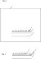
Zunächst wird der CVD-Reaktor 1 als Vorrichtung zu Durchführung der chemischen Gasabscheidung mit dem Siliziumsubstrat 2 samt aufgebrachtem Metallfilm 3 bestückt; z.B. einer Nickelschicht von entweder 5 nm Dicke oder 10 nm Dicke, auf welcher eine Schicht von Diamantkristallen 4 in einer Korngröße von 5 nm bis 40 nm aufgebracht ist. Die Diamantkristalle sind bevorzugt DND (Detonation Nano Diamant)-Kristalle, können aber auch in einem anderen Verfahren als mittels einer Detonation hergestellt worden sein. Durch die hohe Oberflächenenergie des Nickels und der Diamanten entsteht eine gleichmäßige und dichte Verteilung der Diamantkristalle auf dem Nickelfilm. Dasselbe trifft zu für Kupfer. Der Übersichtlichkeit halber ist der CVD-Reaktor 1 nur in
Als CVD Reaktor 1 kann z.B. eine normaler MPCVD-Reaktor (Microwave-Plasma-Chemical-Vapour-Deposition-Reaktor) verwendet werden. Geeignet ist auch ein HFCVD-Reaktor (Hot Filament Chemical Vapour Deposition Reaktor). Ferner eignen sich auch weiterführende Reaktoren, die mit zusätzlichen Mitteln (wie z.B. Laser- oder Ionenbeschuss) Energie an die Aufwachsebene des Diamanten befördern.
1 : Zunächst evakuieren wir die Reaktor-Kammer des CVD-Reaktors 1, um sämtliche atmosphärischen Gase aus der Reaktorkammer zu verbannen. Danach fluten wir, während wir die Temperatur langsam hochfahren, die Kammer zunächst mit Wasserstoff, dem Prozessgas und dann mit Methan, dem Träger des Kohlenstoffs, den wir auf dem Substrat als Diamant abscheiden möchten. Das Verhältnis von Wasserstoff zu Methan beträgt etwa 10 / 1. Die Fließgeschwindigkeit des Wasserstoffs ist etwa 400 sccm und die des Methans etwa 40 sccm, man kann aber auch eine andere Fließgeschwindigkeit und ein anderes Mengenverhältnis zwischen H2 und CH4 wählen. Den Druck in der Reaktor-Kammer halten wir am Anfang noch bei einem sehr niedrigen Niveau von ca. 25 Torr. Im Laufe des Verfahrens erhöhen wir den Druck aber auf bis zu 135 Torr.2 : Wenn wir beim Hochfahren der Temperatur 200 °C erreichen, wachsen die Diamant-Kristalle noch nicht auf, aber das Nickel beginnt langsam in das Silizium des Substrats 2 hinein zu diffundieren und fängt aneine Zwischenschicht 5 aus Nickel-Silizium zu bilden.- Während der nächsten Operationszeit der ersten Stunde bildet sich (
3 ) ab 400°C polykristalliner Nicht-Diamant-Kohlenstoff (Kohlenstoff 6) zwischen den einzelnen Seed-Zellen (Diamantkristalle 4). Dieser wird jedoch von dem Prozess-Wasserstoff mit aufgebrochen und durch das Plasma zu Methan oder anderen Wasserstoff-Kohlenstoff-Gasen umgewandelt. Dabei (4 ) diffundiert auch Kohlenstoff 6 in die Zwischenschicht 5 (Nickel-Silizium- Schicht), bzw. diffundiert wieder heraus. Langsam beginnen die zunächst durcheinander liegenden Diamantkristalle 4 zu wachsen. Dabei wachsen sie bevorzugt in der (110) Orientation oder in der (100) Orientation. Da die (110) orientiert liegenden Kristalle 4 etwas schneller wachsen als die in anderen Richtungen liegenden, bildet sich bald eine beinahe einheitliche Wachstumsorientierung. 5 : Bei einer Temperatur von 750 °C bildet sich zunächst eine polykristalline Schicht 7 von Nicht-Diamant-Kohlenstoff (Kohlenstoff 6)auf den Diamantkristallen 4, die sich jedoch bei noch höherer Temperatur wieder zurückbildet.6 : Unter Aufnahme von Kohlenstoff aus dem Methangas erhalten wir eine Aufwachs-Struktur, bei welcher die schnell wachsenden Kristalle den langsam wachsenden Kristallen die Energie und das Methangas wegnehmen und diese überwuchern.7 und8 : Bei einem weiteren Wachstum bildet sich dann eine mehr oder weniger einheitliche Schicht von schnell wachsenden Diamantkristallen 4, welche alle in derselben Orientierung nach oben wachsen.
1 : First, we evacuate the reactor chamber ofCVD reactor 1 to remove all atmospheric gases from the reactor chamber. Then, while slowly increasing the temperature, we flood the chamber first with hydrogen, the process gas, and then with methane, the carrier of the carbon we want to deposit as diamond on the substrate. The ratio of hydrogen to methane is approximately 10/1. The hydrogen flow rate is approximately 400 sccm and that of methane approximately 40 sccm; however, a different flow rate and a different ratio ofH2 toCH4 can also be selected. We initially keep the pressure in the reactor chamber at a very low level of approximately 25 Torr. Over the course of the process, however, we increase the pressure to up to 135 Torr.2 : When we reach 200 °C during the temperature increase, the diamond crystals do not yet grow, but the nickel slowly begins to diffuse into the silicon of thesubstrate 2 and starts to form anintermediate layer 5 of nickel-silicon.- During the next operating time of the first hour, (
3 ) from 400°C polycrystalline non-diamond carbon (carbon 6) between the individual seed cells (diamond crystals 4). However, this is Process hydrogen is broken up and converted by the plasma into methane or other hydrogen-carbon gases.4 ),carbon 6 also diffuses into the intermediate layer 5 (nickel-silicon layer), or diffuses out again. Thediamond crystals 4, which are initially arranged in a jumbled pattern, slowly begin to grow. They grow preferentially in the (110) orientation or the (100) orientation. Since the (110) orientedcrystals 4 grow somewhat faster than those in other directions, an almost uniform growth orientation soon forms. 5 : At a temperature of 750 °C, apolycrystalline layer 7 of non-diamond carbon (carbon 6) initially forms on thediamond crystals 4, but this layer regresses at an even higher temperature.6 : By absorbing carbon from the methane gas, we obtain a growth structure in which the fast-growing crystals take away the energy and methane gas from the slow-growing crystals and overgrow them.7 and8 : With further growth, a more or less uniform layer of fast-growingdiamond crystals 4 is formed, all of which grow upwards in the same orientation.
In der Grenzschicht können sich kleine Silizium-Nickel Partikel 8 oder polykristallines schwarzes Karbon ablagern, doch sind diese Partikel so klein, dass sie unterhalb der Sichtbarkeitsgrenze mit bloßem Auge liegen. Die Nickelschicht ist inzwischen annähernd oder völlig verschwunden, alles Nickel ist ins Silizium-Substrat diffundiert.Small silicon-
Während wir nach 2 bis 3,5 Stunden noch etwa 10 bis 15% des Diamanten in der Orientierung (111) vorliegen haben, ist nach etwa 10 Stunden das Verhältnis von Diamant in der Orientierung (110) zu Diamant in der Orientierung (111) schon bei nahezu 95 % zu 5%.While after 2 to 3.5 hours we still have about 10 to 15% of the diamond in the orientation (111), after about 10 hours the ratio of diamond in the orientation (110) to diamond in the orientation (111) is already almost 95% to 5%.
Wir können jetzt also schon von einer monokristallinen oder „quasi-monokristallinen“ Diamantschicht bzw. Diamantscheibe sprechen.We can now speak of a monocrystalline or “quasi-monocrystalline” diamond layer or diamond disc.
Chemisch gesehen passiert folgendes, was sowohl für Ausführungsvariante 1) als auch für Ausführungsvariante 2) zutrifft:
- Von dem Prozessgas (oder Katalysator-Gas) H2 zerfällt ein Wasserstoff-Molekül und die beiden Wasserstoff-Atome lagern sich an zwei Kohlenstoff-Atomen der Diamantscheibe oder des Diamant-Seeds an, die ihrerseits damit wieder ihre Bindung zueinander aufgeben.
- A hydrogen molecule from the process gas (or catalyst gas) H2 decomposes and the two hydrogen atoms attach themselves to two carbon atoms of the diamond disc or diamond seed, which in turn release their bond to each other.
Dann spaltet sich ein Wasserstoff-Atom vom Methan-Gas ab, bildet mit dem Wasserstoff-Atom, welches sich temporär mit einem Kohlenstoffatom des Diamantgitters verbunden hatte, ein H2-Molekül und setzt damit das Kohlenstoffatom frei, welches sich nun mit der freien Valenz des Kohlenstoff-Atoms des Methans verbinden kann.Then a hydrogen atom splits off from the methane gas, forms an H2 molecule with the hydrogen atom that had temporarily bonded to a carbon atom of the diamond lattice, and thus releases the carbon atom, which can now bond with the free valence of the carbon atom of the methane.
Derselbe Prozess findet auch mit dem zweiten Kohlenstoffatom statt, welches eine freie Valenz hat, sobald sich ein H-Atom entfernt hat.The same process also occurs with the second carbon atom, which has a free valence once one H atom has been removed.
Schließlich entreißt das H2-Gas-Plasma den halbwegs angebundenen Methan-Gas-Molekülen jeweils ein H-Atom, woraufhin sich die beiden freien Valenzen der beiden Kohlenstoffatome des Diamant miteinander verbinden können.Finally, the H2 gas plasma tears one H atom from each of the halfway bound methane gas molecules, whereupon the two free valences of the two carbon atoms of the diamond can bond with each other.
Somit sind zwei neue Kohlenstoffatome am Diamant angedockt, der Diamant ist ein kleines bisschen gewachsen.Thus, two new carbon atoms are docked to the diamond, and the diamond has grown a little bit.
Die Aufwachsgeschwindigkeit beträgt je nach Temperatur und Gasgemisch bis zu 8 µm / h, teilweise bis zu 10 µm /h.Depending on the temperature and gas mixture, the growth rate is up to 8 µm / h, sometimes up to 10 µm / h.
Ein nachträgliches „Annealing“ der Diamantscheibe, wie dies bei der Herstellung synthetischer Diamanten üblich ist, also das „Auskristallisieren“ der Diamant-Struktur und die Farbverbesserung im HPHT-Reaktor, ist nicht möglich. Das doppelstrukturierte Quarz-Diamant-Glas würde diese Prozedur ggf. nicht unbeschadet überstehen. Deswegen lässt man die Aufwachsgeschwindigkeit in diesem Verfahren eher niedrig, wodurch eine bessere Farbe und reinere Struktur des Diamant-Teils entstehen und das nachträgliche auskristallisieren im Annealing mittels HPHT Verfahren überflüssig macht.Subsequent annealing of the diamond disc, as is common in the production of synthetic diamonds—that is, the "crystallization" of the diamond structure and color enhancement in the HPHT reactor—is not possible. The double-structured quartz-diamond glass might not survive this procedure unscathed. Therefore, the growth rate in this process is kept relatively low, resulting in a better color and purer structure of the diamond part and eliminating the need for subsequent crystallization in the annealing process using the HPHT process.
Die fertige Diamant-Scheibe wird nach dem Aufwachsen vorzugsweise auf der den zugänglichen Oberflächen mechanisch poliert, um eine absolut glatte Oberfläche aufzuweisenAfter growth, the finished diamond disc is mechanically polished, preferably on the accessible surfaces, in order to have an absolutely smooth surface
Wenn wir in dem Verfahren zur Ausführungsvariante 1) zwischen der Schicht Trägerscheibe 2 und Metallfilm 3 noch einen Zusatzfilm, zum Beispiel eine dünne Schicht Silizium, einbauen, z.B. etwa zwischen 5 nm und 10 nm, dann bewirkt dieser Zusatzfilm, dass das polykristalline „non-diamond-carbon“ (NDC) in das Silizium eingebaut wird (SiC), um sich dann im Plasmaprozess wieder aufzulösen. Daher kann der Zusatzfilm eine verbesserte optische Qualität des Bauteils bewirken. Des Weiteren stellt der Zusatzfilm auf Grund der minimalen Dicke einen Film dar, der eine gewisse Elastizität hat und daher den mechanischen Stress auf Grund der verschiedenen Ausdehnungskoeffizienten von Quarzglas und Diamant reduziert.If, in the process for embodiment 1), we incorporate an additional film, for example a thin layer of silicon, between the
Für das Verfahren zur Herstellung der Diamatscheibe ohne Trägerscheibe (Ausführungsvariante 2) nehmen wir bevorzugt einen normalen Wafer für Halbleiter aus reinem Silizium. Silizium hat schon mal die perfekte kristallographische Struktur, ähnlich derer von Diamant, also die flächenzentrierte kubische Kristallstruktur. Außerdem hat der Halbleiter-Wafer aus reinem Silizium einen Ausdehnungskoeffizienten von nur 2,5 × 10⁻⁶ K-1. Das ist zwar immer noch das Zweieinhalbfache des Ausdehnungskoeffizienten von synthetischem Diamant (1,0 × 10⁻⁶ K-1). Doch ist dies, abgesehen von Spezialgläsern wie reinem Quarzglas, ein Ausdehnungskoeffizient, der dem von Diamant sehr nahekommt. Zum Vergleich: Saphir hat 6,0 × 10⁻⁶ K-1, Floatglas hat 9,2 × 10⁻⁶ K-1.For the process for producing the diamond wafer without a carrier wafer (version 2), we prefer to use a standard semiconductor wafer made of pure silicon. Silicon already has a perfect crystallographic structure, similar to that of diamond—a face-centered cubic crystal structure. Furthermore, the semiconductor wafer made of pure silicon has an expansion coefficient of only 2.5 × 10⁻⁶ K-1 . This is still two and a half times the expansion coefficient of synthetic diamond (1.0 × 10⁻⁶ K-1 ). However, with the exception of special glasses such as pure quartz glass, this is a coefficient of expansion that is very close to that of diamond. For comparison: sapphire has 6.0 × 10⁻⁶ K-1 , and float glass has 9.2 × 10⁻⁶ K-1 .
Auf den Wafer bringen wir den Metallfilm z.B. aus Nickel auf. Die Schichtdicke sollte etwa 5 nm oder 10 nm betragen. Nickel hat nicht nur dieselbe kristallographische Struktur wie Diamant (den flächenzentrierten Kubus), sondern die Größe der Elementarzelle von Nickel entspricht mit nur 1,5 % Abweichung der Größe der Elementarzelle von Diamant (Nickel 3,52 Å, Diamant 3,57 Å). Wir beschichten dann das Substrat aus Silizium/Metallfilm mit DND-Diamantpulver. Danach wachsen wir im CVD-Verfahren synthetischen Diamant auf das Substrat auf, vorzugsweise in der kristallographischen Orientierung (110) oder (100). Die Aufwachsgeschwindigkeit entspricht ca. 8 µm/h. Wenn wir ein Diamantglas von ca. 1 mm Dicke produzieren möchten, benötigen wir also etwa 150 Stunden. Wir nehmen also das mit dem Diamantfilm beschichtete Substrat nach 6 Tagen wieder aus dem Reaktor. Wir entfernen zunächst mittels Laser den polykristallinen Kohlenstoff an den Rändern des Diamantglases. Danach schneiden wir das Glas mittels Laser auf die genaue gewünschte Größe und Form. Danach schleifen wir es von beiden Seiten ab, bis es genau die gewünschte Dicke besitzt.We apply a metal film, for example, made of nickel, to the wafer. The layer thickness should be approximately 5 nm or 10 nm. Not only does nickel have the same crystallographic structure as diamond (the face-centered cube), but the size of the nickel unit cell corresponds to the size of the diamond unit cell, with only a 1.5% deviation (nickel 3.52 Å, diamond 3.57 Å). We then coat the silicon/metal film substrate with DND diamond powder. We then grow synthetic diamond onto the substrate using a CVD process, preferably in the crystallographic orientation (110) or (100). The growth rate is approximately 8 µm/h. Therefore, if we want to produce a diamond glass approximately 1 mm thick, we need approximately 150 hours. We remove the substrate coated with the diamond film from the reactor after 6 days. We first use a laser to remove the polycrystalline carbon from the edges of the diamond glass. We then laser cut the glass to the exact desired size and shape. We then sand it on both sides until it reaches the exact thickness you require.
Danach wird auf der Innenseite vorzugsweise eine Beschichtung oder Mehrfachbeschichtung aufgetragen.Afterwards, a coating or multiple coatings are preferably applied to the inside.
BezugszeichenlisteList of reference symbols
- 11
- CVD-ReaktorCVD reactor
- 22
- Siliziumsubstrat (Substrat)Silicon substrate (substrate)
- 33
- Metallfilmmetal film
- 44
- DiamantkristalleDiamond crystals
- 55
- Nickel-Silizium-ZwischenschichtNickel-silicon interlayer
- 66
- Kohlenstoffcarbon
- 77
- polykristalline Schichtpolycrystalline layer
- 88
- Silizium-Nickel PartikelSilicon-nickel particles
Claims (19)
Translated fromGermanPriority Applications (2)
| Application Number | Priority Date | Filing Date | Title |
|---|---|---|---|
| DE102023133275.9ADE102023133275A1 (en) | 2023-11-28 | 2023-11-28 | Process for producing a transparent, scratch-resistant component |
| PCT/EP2024/083994WO2025114481A2 (en) | 2023-11-28 | 2024-11-28 | Method for producing a transparent, scratch-resistant component |
Applications Claiming Priority (1)
| Application Number | Priority Date | Filing Date | Title |
|---|---|---|---|
| DE102023133275.9ADE102023133275A1 (en) | 2023-11-28 | 2023-11-28 | Process for producing a transparent, scratch-resistant component |
Publications (1)
| Publication Number | Publication Date |
|---|---|
| DE102023133275A1true DE102023133275A1 (en) | 2025-05-28 |
Family
ID=93797038
Family Applications (1)
| Application Number | Title | Priority Date | Filing Date |
|---|---|---|---|
| DE102023133275.9APendingDE102023133275A1 (en) | 2023-11-28 | 2023-11-28 | Process for producing a transparent, scratch-resistant component |
Country Status (2)
| Country | Link |
|---|---|
| DE (1) | DE102023133275A1 (en) |
| WO (1) | WO2025114481A2 (en) |
Citations (6)
| Publication number | Priority date | Publication date | Assignee | Title |
|---|---|---|---|---|
| US20040069209A1 (en)* | 2002-08-27 | 2004-04-15 | Board Of Trustees Of Michigan State University | Heteroepitaxial diamond and diamond nuclei precursors |
| DE10320133A1 (en)* | 2003-05-06 | 2004-12-02 | Universität Augsburg | Single crystal diamond layer and process for its production |
| JP2006096640A (en)* | 2004-09-30 | 2006-04-13 | Kobe Steel Ltd | Substrate for synthesizing single crystal diamond and method for producing single crystal diamond film |
| CN113430640A (en)* | 2021-06-23 | 2021-09-24 | 西安交通大学 | Method for preparing heteroepitaxial single crystal diamond by using Pt metal as Ir buffer layer |
| CN114892141A (en)* | 2022-05-10 | 2022-08-12 | 化合积电(厦门)半导体科技有限公司 | Method for manufacturing diamond diaphragm |
| DE102022205081A1 (en)* | 2022-05-20 | 2023-11-23 | Universität Augsburg, Körperschaft des öffentlichen Rechts | Method, substrate, device and their use for the synthesis of flat single-crystalline diamonds |
Family Cites Families (8)
| Publication number | Priority date | Publication date | Assignee | Title |
|---|---|---|---|---|
| JP3728465B2 (en)* | 1994-11-25 | 2005-12-21 | 株式会社神戸製鋼所 | Method for forming single crystal diamond film |
| US5686152A (en)* | 1995-08-03 | 1997-11-11 | Johnson; Linda F. | Metal initiated nucleation of diamond |
| JP3728467B2 (en)* | 1995-08-04 | 2005-12-21 | 株式会社神戸製鋼所 | Method for forming single crystal diamond film |
| US7132309B2 (en)* | 2003-04-22 | 2006-11-07 | Chien-Min Sung | Semiconductor-on-diamond devices and methods of forming |
| US10494713B2 (en)* | 2015-04-16 | 2019-12-03 | Ii-Vi Incorporated | Method of forming an optically-finished thin diamond film, diamond substrate, or diamond window of high aspect ratio |
| JP7078947B2 (en)* | 2017-02-06 | 2022-06-01 | 信越化学工業株式会社 | A base substrate for diamond film formation and a method for manufacturing a diamond substrate using the substrate. |
| CN110670126B (en)* | 2019-09-30 | 2021-03-23 | 长沙新材料产业研究院有限公司 | Diamond with cantilever structure and preparation method thereof |
| US11753740B2 (en)* | 2019-11-18 | 2023-09-12 | Shin-Etsu Chemical Co., Ltd. | Diamond substrate and method for manufacturing the same |
- 2023
- 2023-11-28DEDE102023133275.9Apatent/DE102023133275A1/enactivePending
- 2024
- 2024-11-28WOPCT/EP2024/083994patent/WO2025114481A2/enactivePending
Patent Citations (6)
| Publication number | Priority date | Publication date | Assignee | Title |
|---|---|---|---|---|
| US20040069209A1 (en)* | 2002-08-27 | 2004-04-15 | Board Of Trustees Of Michigan State University | Heteroepitaxial diamond and diamond nuclei precursors |
| DE10320133A1 (en)* | 2003-05-06 | 2004-12-02 | Universität Augsburg | Single crystal diamond layer and process for its production |
| JP2006096640A (en)* | 2004-09-30 | 2006-04-13 | Kobe Steel Ltd | Substrate for synthesizing single crystal diamond and method for producing single crystal diamond film |
| CN113430640A (en)* | 2021-06-23 | 2021-09-24 | 西安交通大学 | Method for preparing heteroepitaxial single crystal diamond by using Pt metal as Ir buffer layer |
| CN114892141A (en)* | 2022-05-10 | 2022-08-12 | 化合积电(厦门)半导体科技有限公司 | Method for manufacturing diamond diaphragm |
| DE102022205081A1 (en)* | 2022-05-20 | 2023-11-23 | Universität Augsburg, Körperschaft des öffentlichen Rechts | Method, substrate, device and their use for the synthesis of flat single-crystalline diamonds |
Also Published As
| Publication number | Publication date |
|---|---|
| WO2025114481A2 (en) | 2025-06-05 |
| WO2025114481A3 (en) | 2025-10-02 |
Similar Documents
| Publication | Publication Date | Title |
|---|---|---|
| DE102014104799B4 (en) | Substrate with a coating to increase scratch resistance, process for its production and its use | |
| DE19543723C2 (en) | Process for the production of single crystal diamond films | |
| DE69411777T2 (en) | Single crystal diamond and process for its manufacture | |
| DE69124881T2 (en) | Diamond-like carbon coatings | |
| DE69003557T2 (en) | Diamond breeding. | |
| DE69504896T2 (en) | Synthetic diamond layer with reduced bending and process for its production | |
| DE102009022224A1 (en) | Process for producing epitaxial silicon wafers | |
| DE102005045338A1 (en) | Epitaxial silicon wafer and process for producing epitaxially coated silicon wafers | |
| AT411070B (en) | METHOD FOR PRODUCING A SUBSTRATE WITH A POLYCRYSTALLINE DIAMOND LAYER | |
| DE10302342A1 (en) | Production of substrate used in the production of mask or optical component comprises preparing a base layer, applying a first covering layer on the base layer, and post-treating the covering layer | |
| DE102005060883A1 (en) | Vacuum process and assembly to manufacture diamond-coated spheres for ball bearing assembly | |
| DE3112604A1 (en) | METHOD FOR PRODUCING AN AMORPHOUS SILICON FILM | |
| WO2021032493A1 (en) | Temperable coatings having diamond-like carbon and deposition by means of high-power impulse magnetron sputtering | |
| DE10211312A1 (en) | Epitaxial coating applying method of semiconductor wafer in chemical vapor deposition reactor, involves exposing back surface of semiconductor wafer to ejection gas containing specific amount of hydrogen | |
| DE102023133275A1 (en) | Process for producing a transparent, scratch-resistant component | |
| DE19528329A1 (en) | X-ray transparent layer material, process for its production and its use | |
| DE3877407T2 (en) | PRODUCTION OF A DEVICE BY X-RAY RAY LITHOGRAPHY BY MEANS OF A STABLE BORNITRIDE MASK. | |
| DE102013004558B4 (en) | Method for producing a surface-strained sapphire disk, surface-strained sapphire disk and electrical device with a transparent cover | |
| DE3882856T2 (en) | Production of a polycrystalline layer. | |
| DE3152307A1 (en) | USE OF METALLIC GLASSES FOR FABRICATION OF STRUCTURES WITH SUBMICRON DIMENSIONS | |
| EP3779526A1 (en) | Method of manufacturing an aluminum layer and optical element | |
| DE102015200692B4 (en) | Epitaxial diamond layer and process for its preparation | |
| DE102004010377A1 (en) | Production of substrate wafers for low-defect semiconductor components, their use, and components obtained therewith | |
| DE102012200454A1 (en) | Method for manufacturing reflective optical element for extreme ultraviolet lithography for manufacturing of semiconductor devices, involves providing substrate, applying releasing layer, and applying layer with optical function | |
| DE102023133273A1 (en) | watch glass |
Legal Events
| Date | Code | Title | Description |
|---|---|---|---|
| R012 | Request for examination validly filed |