DE102021214166A1 - Radar sensor and a manufacturing process - Google Patents
Radar sensor and a manufacturing processDownload PDFInfo
- Publication number
- DE102021214166A1 DE102021214166A1DE102021214166.8ADE102021214166ADE102021214166A1DE 102021214166 A1DE102021214166 A1DE 102021214166A1DE 102021214166 ADE102021214166 ADE 102021214166ADE 102021214166 A1DE102021214166 A1DE 102021214166A1
- Authority
- DE
- Germany
- Prior art keywords
- circuit board
- signals
- radar sensor
- board
- recess
- Prior art date
- Legal status (The legal status is an assumption and is not a legal conclusion. Google has not performed a legal analysis and makes no representation as to the accuracy of the status listed.)
- Pending
Links
Images


Classifications
- H—ELECTRICITY
- H01—ELECTRIC ELEMENTS
- H01Q—ANTENNAS, i.e. RADIO AERIALS
- H01Q1/00—Details of, or arrangements associated with, antennas
- H01Q1/27—Adaptation for use in or on movable bodies
- H01Q1/32—Adaptation for use in or on road or rail vehicles
- H01Q1/3208—Adaptation for use in or on road or rail vehicles characterised by the application wherein the antenna is used
- H01Q1/3233—Adaptation for use in or on road or rail vehicles characterised by the application wherein the antenna is used particular used as part of a sensor or in a security system, e.g. for automotive radar, navigation systems
- H—ELECTRICITY
- H01—ELECTRIC ELEMENTS
- H01P—WAVEGUIDES; RESONATORS, LINES, OR OTHER DEVICES OF THE WAVEGUIDE TYPE
- H01P3/00—Waveguides; Transmission lines of the waveguide type
- H01P3/12—Hollow waveguides
- H01P3/121—Hollow waveguides integrated in a substrate
- H—ELECTRICITY
- H01—ELECTRIC ELEMENTS
- H01Q—ANTENNAS, i.e. RADIO AERIALS
- H01Q13/00—Waveguide horns or mouths; Slot antennas; Leaky-waveguide antennas; Equivalent structures causing radiation along the transmission path of a guided wave
- H01Q13/10—Resonant slot antennas
- H01Q13/18—Resonant slot antennas the slot being backed by, or formed in boundary wall of, a resonant cavity ; Open cavity antennas
- H—ELECTRICITY
- H05—ELECTRIC TECHNIQUES NOT OTHERWISE PROVIDED FOR
- H05K—PRINTED CIRCUITS; CASINGS OR CONSTRUCTIONAL DETAILS OF ELECTRIC APPARATUS; MANUFACTURE OF ASSEMBLAGES OF ELECTRICAL COMPONENTS
- H05K1/00—Printed circuits
- H05K1/02—Details
- H05K1/0213—Electrical arrangements not otherwise provided for
- H05K1/0237—High frequency adaptations
- H05K1/0243—Printed circuits associated with mounted high frequency components
- H—ELECTRICITY
- H05—ELECTRIC TECHNIQUES NOT OTHERWISE PROVIDED FOR
- H05K—PRINTED CIRCUITS; CASINGS OR CONSTRUCTIONAL DETAILS OF ELECTRIC APPARATUS; MANUFACTURE OF ASSEMBLAGES OF ELECTRICAL COMPONENTS
- H05K1/00—Printed circuits
- H05K1/02—Details
- H05K1/14—Structural association of two or more printed circuits
- H05K1/144—Stacked arrangements of planar printed circuit boards
- H—ELECTRICITY
- H05—ELECTRIC TECHNIQUES NOT OTHERWISE PROVIDED FOR
- H05K—PRINTED CIRCUITS; CASINGS OR CONSTRUCTIONAL DETAILS OF ELECTRIC APPARATUS; MANUFACTURE OF ASSEMBLAGES OF ELECTRICAL COMPONENTS
- H05K2201/00—Indexing scheme relating to printed circuits covered by H05K1/00
- H05K2201/04—Assemblies of printed circuits
- H05K2201/042—Stacked spaced PCBs; Planar parts of folded flexible circuits having mounted components in between or spaced from each other
- H—ELECTRICITY
- H05—ELECTRIC TECHNIQUES NOT OTHERWISE PROVIDED FOR
- H05K—PRINTED CIRCUITS; CASINGS OR CONSTRUCTIONAL DETAILS OF ELECTRIC APPARATUS; MANUFACTURE OF ASSEMBLAGES OF ELECTRICAL COMPONENTS
- H05K2201/00—Indexing scheme relating to printed circuits covered by H05K1/00
- H05K2201/09—Shape and layout
- H05K2201/09009—Substrate related
- H05K2201/09072—Hole or recess under component or special relationship between hole and component
Landscapes
- Engineering & Computer Science (AREA)
- Microelectronics & Electronic Packaging (AREA)
- Computer Security & Cryptography (AREA)
- Radar, Positioning & Navigation (AREA)
- Remote Sensing (AREA)
- Radar Systems Or Details Thereof (AREA)
Abstract
Translated fromGerman
Description
Translated fromGermanDie vorliegende Erfindung betrifft einen Radarsensor sowie ein Herstellungsverfahren zum Herstellen eines erfindungsgemäßen Radarsensors.The present invention relates to a radar sensor and a production method for producing a radar sensor according to the invention.
Technologischer HintergrundTechnological background
Moderne Fortbewegungsmittel wie Kraftfahrzeuge oder Motorräder werden zunehmend mit Fahrerassistenzsystemen ausgerüstet, welche mit Hilfe von Sensorsystemen die Umgebung erfassen, Verkehrssituationen erkennen und den Fahrer unterstützen können, z. B. durch einen Brems- oder Lenkeingriff oder durch die Ausgabe einer optischen oder akustischen Warnung. Als Sensorsysteme zur Umgebungserfassung werden regelmäßig Radarsensoren, Lidarsensoren, Kamerasensoren oder dergleichen eingesetzt. Aus den durch die Sensoren ermittelten Sensordaten können anschließend Rückschlüsse auf die Umgebung gezogen werden. Die Umgebungserfassung mittels Radarsensoren basiert auf der Aussendung von gebündelten elektromagnetischen Wellen und deren Reflexion, z. B. durch andere Verkehrsteilnehmer, Hindernissen auf der Fahrbahn oder die Randbebauung der Fahrbahn. Die Erfassung von Fußgängern wird oftmals mit Kamerasensoren durchgeführt, jedoch kommen hierbei auch zunehmend Radarsensoren zum Einsatz.Modern means of transport such as motor vehicles or motorcycles are increasingly being equipped with driver assistance systems which use sensor systems to detect the environment, recognize traffic situations and support the driver, e.g. B. by a braking or steering intervention or by the output of a visual or acoustic warning. Radar sensors, lidar sensors, camera sensors or the like are regularly used as sensor systems for detecting the surroundings. From the sensor data determined by the sensors, conclusions can then be drawn about the environment. Environment detection using radar sensors is based on the emission of bundled electromagnetic waves and their reflection, e.g. B. by other road users, obstacles on the road or the edge of the road. Pedestrians are often detected using camera sensors, but radar sensors are also increasingly being used here.
Für Systeme der oben beschriebenen Art werden Radarsensoren eingesetzt, häufig auch in Fusion mit Sensoren anderer Technologie, wie z. B. Kamera- oder Lidarsensoren. Radarsensoren haben u. a. den Vorteil, dass sie auch bei schlechten Wetterbedingungen zuverlässig arbeiten und neben dem Abstand von Objekten auch direkt deren radiale Relativgeschwindigkeit über den Dopplereffekt messen können. Als Sendefrequenzen werden dabei in der Regel 24 GHz, 77 GHz und 79 GHz eingesetzt. Durch den zunehmenden funktionalen Umfang solcher Systeme erhöhen sich permanent die Anforderungen, insbesondere an die maximale Detektionsreichweite. Gleichzeitig findet aber dennoch ein starker Preisverfall statt. Neben der Umgebungserfassung von Kraftfahrzeugen für Systeme der oben beschriebenen Art rückt mittlerweile auch die Innenraumüberwachung von Kraftfahrzeugen in den Fokus, z. B. zur Erkennung, welche Sitze belegt sind; dabei werden Frequenzen im Bereich 60 GHz eingesetzt.Radar sensors are used for systems of the type described above, often in combination with sensors of other technologies, such as e.g. B. camera or lidar sensors. Radar sensors have i.a. the advantage that they work reliably even in poor weather conditions and, in addition to the distance from objects, can also directly measure their radial relative speed using the Doppler effect. As a rule, 24 GHz, 77 GHz and 79 GHz are used as transmission frequencies. Due to the increasing functional scope of such systems, the requirements are constantly increasing, especially with regard to the maximum detection range. At the same time, however, there is a sharp fall in prices. In addition to detecting the surroundings of motor vehicles for systems of the type described above, the interior monitoring of motor vehicles is now also coming into focus, e.g. B. to identify which seats are occupied; frequencies in the 60 GHz range are used.
Ein zentrales Element jedes Radarsensors ist die Antenne, sie definiert maßgeblich die Performance und den Preis des Radarsensors. Aktuell werden die Antennen meist in Planartechnologie auf einer Hochfrequenzplatine realisiert, z. B. als Patchantennen.A central element of every radar sensor is the antenna, which largely defines the performance and price of the radar sensor. Currently, the antennas are mostly realized in planar technology on a high-frequency circuit board, e.g. B. as patch antennas.
Nachteilig an einer solchen Antennenrealisierung sind Verluste in Zuleitungen und Antennen (was die Reichweite limitiert) sowie ein hoher Kostenaufwand einer solchen Platine, wobei z. B. die Material- und Prozesskosten deutlich höher sind als bei der Verwendung von Standard-PCB-Materialen.Disadvantages of such an antenna implementation are losses in feed lines and antennas (which limits the range) and the high cost of such a circuit board, with z. B. the material and process costs are significantly higher than when using standard PCB materials.
Gattungsgemäße Antennen bestehen in der Regel (vollständig oder teilweise) aus einer Leiterplatte bzw. PCB (Printed Circuit Board) mit einer insbesondere geätzten Metallstruktur auf einem HF-Substrat und/oder einem Formteil aus Kunststoff. Daraus können Nachteile entstehen, wie z. B. hohe Kosten durch spezielle HF-Substrate, schwankende Material Eigenschaften oder sehr anspruchsvolle Fertigungstoleranzen eines Formteiles. Außerdem ist die Schichtdicke der Oberflächenmetallisierung des Formteils relativ dünn (z. B. typischerweise dünner als 5µm insbesondere inklusive Haftvermittler, Antioxidationsschicht, „Finishing“ für Lötung oder dergleichen), wodurch die HF-Performance, die Lötqualität oder dergleichen beeinträchtigt werden können, d. h. der Radarsensor weniger zuverlässig arbeitet.Generic antennas generally consist (completely or partially) of a printed circuit board or PCB (printed circuit board) with an etched metal structure in particular on an HF substrate and/or a molded part made of plastic. This can result in disadvantages such as B. high costs due to special HF substrates, fluctuating material properties or very demanding manufacturing tolerances of a molded part. In addition, the layer thickness of the surface metallization of the molded part is relatively thin (e.g. typically thinner than 5 µm, in particular including adhesion promoter, antioxidant layer, "finishing" for soldering or the like), which can affect the HF performance, the soldering quality or the like, i. H. the radar sensor works less reliably.
Druckschriftlicher Stand der TechnikPrinted state of the art
Aus der
Aufgabe der vorliegenden ErfindungObject of the present invention
Ausgehend vom Stand der Technik besteht die Aufgabe der vorliegenden Erfindung nunmehr darin, einen Radarsensor mit verbesserter Performance und Zuverlässigkeit sowie ein Herstellungsverfahren eines derartigen Radarsensors zur Verfügung zu stellen, mit dem die Nachteile aus dem Stand der Technik in einfacher und kostengünstiger Weise überwunden sind.Proceeding from the prior art, the object of the present invention is now to provide a radar sensor with improved performance and reliability and a manufacturing method for such a radar sensor, with which the disadvantages of the prior art are overcome in a simple and cost-effective manner.
Lösung der Aufgabesolution of the task
Die vorstehende Aufgabe wird durch die gesamte Lehre des Anspruchs 1 sowie des nebengeordneten Anspruchs gelöst. Zweckmäßige Ausgestaltungen der Erfindung sind in den Unteransprüchen beansprucht.The above object is achieved by the entire teaching of
Der erfindungsgemäße Radarsensor dient insbesondere zur Objekterkennung und kann praktischerweise im Automotive bzw. Fahrzeugbereich eingesetzt werden. Der Radarsensor umfasst dabei eine erste Platine mit mindestens einem HF-Bauteil bzw. Hochfrequenzbauteil zum Erzeugen und/oder Empfangen von HF-Signalen (bzw. Radarsignale) und mindestens einer Öffnung zum Ein- und/oder Auskoppeln der HF-Signale, und eine zweite Platine, wobei die erste Platine und zweite Platine zumindest teilweise metallisiert sind, die erste Platine und/oder zweite Platine zumindest eine, insbesondere longitudinale, Ausnehmung aufweisen, und die erste Platine oder die zweite Platine zumindest eine Öffnung zum Abstrahlen und/oder Empfangen der HF-Signale aufweist. Ferner wird mindestens ein Wellenleiter durch die Ausnehmung bzw. die Ausnehmungen in der ersten Platine und/oder der zweiten Platine sowie die Anordnung der Platinen zueinander gebildet, d. h. der Wellenleiter entsteht durch den, insbesondere luftgefüllten, Raum innerhalb der Ausnehmung(en), der durch die insbesondere metallisierte Wandung der Ausnehmung in der ersten und/oder zweiten Platine entsteht. Durch die spezielle Anordnung der Platinen und den/der Ausnehmung(en) darin entsteht somit eine Wellenleiterantenne bzw. eine Hohlleiterschlitzantenne, welche die Ausnehmung sowie die Öffnung zum Abstrahlen und/oder Empfangen der HF-Signale umfasst.The radar sensor according to the invention is used in particular for object recognition and can be used practically in the automotive or vehicle sector. The radar sensor includes a first circuit board with at least one HF component or high-frequency component for generating and/or receiving HF signals (or radar signals) and at least one opening for coupling and/or decoupling the HF signals, and a second Circuit board, wherein the first circuit board and second circuit board are at least partially metallized, the first circuit board and/or second circuit board have at least one, in particular longitudinal, recess, and the first circuit board or the second circuit board has at least one opening for radiating and/or receiving the RF -Has signals. Furthermore, at least one waveguide is formed by the recess or the recesses in the first circuit board and/or the second circuit board and the arrangement of the circuit boards relative to one another, d. H. the waveguide is created by the space, in particular air-filled, within the recess(es) which is created by the metalized wall of the recess in the first and/or second circuit board. The special arrangement of the circuit boards and the recess(es) therein results in a waveguide antenna or a waveguide slot antenna, which includes the recess and the opening for radiating and/or receiving the HF signals.
In bevorzugter Weise beinhalten die Platinen des erfindungsgemäßen Radarsensors kein HF-Substrat. Dadurch, dass für die Platinen nicht zwangsläufig HF-Substrat verwendet werden muss, ist der erfindungsgemäße Radarsensor besonders kostengünstig mit geringem Herstellungs- und Zeitaufwand herzustellen. Ferner können die Ausnehmungen in einfacher Weise während des Herstellungsprozesses der Platine mit gefertigt werden, wodurch der Zeit- und Kostenaufwand in besonderem Maße verringert wird. Zudem kann die Platine dadurch mechanische als auch elektromagnetische Funktionen erfüllen.The printed circuit boards of the radar sensor according to the invention preferably contain no HF substrate. Due to the fact that an HF substrate does not necessarily have to be used for the printed circuit boards, the radar sensor according to the invention can be produced particularly cost-effectively with little outlay in terms of production and time. Furthermore, the recesses can also be produced in a simple manner during the production process of the circuit board, as a result of which the expenditure of time and money is reduced to a particular extent. In addition, the circuit board can thus fulfill mechanical as well as electromagnetic functions.
Als HF-Substrat im Sinne der Erfindung wird ein Substrat verstanden, das speziell auf die Anwendung im Hochfrequenzbereich optimierte und konstante Parameter aufweist. Diese Parameter sind unter anderem eine konstante Permittivität sowie ein möglichst kleiner Verlustwinkel. Der Wert des Verlustwinkels gängiger HF-Substrate beträgt in der Regel bei 10 GHz 0,005 oder weniger.An HF substrate within the meaning of the invention is understood to be a substrate that has constant parameters that are specifically optimized for use in the high-frequency range. These parameters include a constant permittivity and the smallest possible loss angle. The value of the loss angle of common RF substrates is typically 0.005 or less at 10 GHz.
Als Platine im Sinne der Erfindung sind alle Arten von Leiterplatten umfasst, wie z. B. Leiterkarten oder gedruckte Schaltungen (PCB, Printed Circuit Board), welche als Träger für elektronische Bauteile verwendet werden. Die Leiterplatten umfassen dabei ein elektrisch isolierendes Material und in der Regel daran haftende, leitende Verbindungen (sogenannte Leiterbahnen). Als isolierendes Material kann z. B. faserverstärkter Kunststoff oder Hartpapier (insbesondere aus Phenoplast: Faserverbundwerkstoff aus Papier und Phenol-Formaldehyd-Kunstharz) verwendet werden. Die Leiterbahnen werden zumeist aus einer dünnen Schicht Kupfer geätzt, mit einer Dicke im Bereich von z. B. 10-50 µm. Darauf können dann Bauelemente auf Lötflächen (Pads) oder in Lötaugen gelötet werden, z. B. Mikrochips, HF-Chips oder HF-Bauteile, Sende- und Empfangsantennen. Die Leiterplattenarten reichen von einseitigen Leiterplatten über Multilayer bis hin zu Sondertechniken. Als Platinen können dabei sämtliche aus dem Stand der Technik bekannte Platinenarten- und/oder -materialien eingesetzt werden, wie z. B. Standardleiterplatten, einseitige und zweiseitige Leiterplatten, Multilayerplatten mit mehreren Lagen, Flexlam, Dünnstleiterplatten, Dickkupferleiterplatten, beschichtete Leiterplatten, Leiterplatten auf Glas, HDI (High-Density-Interconnect)-Leiterplatten, SBU (Sequential Build Up)-Leiterplatten, LBA (Leiterbild-Aufbau)-Leiterplatten, IMS (Insulated Metal Substrate)-Leiterplatten oder dergleichen. Durch die Auswahl eines verlustbehafteten Leiterplattenmaterials können unerwünschte Substratwellen unterdrückt werden, wodurch es zu weniger Störungen im Bereich der Antenne oder im Richtdiagramm kommt. Ferner kann durch eine geeignete Auswahl von Platinensubstraten bzw. Materialien der „CTE-mismatch“ im Radarsensor gut balanciert werden, insbesondere können erste und zweite Platine aus gleichem oder unterschiedlichem Material gefertigt sein. Gemäß einer bevorzugten Ausgestaltung der Erfindung kann mindestens eine der Platinen ein Feuerwiderstandsmaterial und/oder ein Bismaleimidtrizinharz und/oder ein Polymidmaterial und/oder ein Epoxidmatrixmaterial und/oder dergleichen umfassen, wobei die Verlustwinkel dieser Materialen größer als 0,005 bei 10 GHz sein sollten.All types of printed circuit boards are included as circuit boards within the meaning of the invention, e.g. As circuit boards or printed circuits (PCB, Printed Circuit Board), which are used as a carrier for electronic components. The printed circuit boards comprise an electrically insulating material and, as a rule, conductive connections (so-called conductor tracks) adhering thereto. As an insulating material z. B. fiber-reinforced plastic or laminated paper (especially from phenolic: fiber composite material made of paper and phenol-formaldehyde resin) can be used. The conductor tracks are usually etched from a thin layer of copper with a thickness in the range of e.g. B. 10-50 µm. Components can then be soldered on soldering surfaces (pads) or in soldering eyes, e.g. B. microchips, HF chips or HF components, transmitting and receiving antennas. The circuit board types range from single-sided circuit boards to multilayer and special technologies. All types and/or materials of circuit boards known from the prior art can be used as circuit boards, such as e.g. B. Standard printed circuit boards, single-sided and double-sided printed circuit boards, multilayer boards with several layers, Flexlam, thin printed circuit boards, thick copper printed circuit boards, coated printed circuit boards, printed circuit boards on glass, HDI (high-density interconnect) printed circuit boards, SBU (sequential build up) printed circuit boards, LBA (circuit diagram -Construction) circuit boards, IMS (Insulated Metal Substrate) circuit boards or the like. By selecting a lossy circuit board material, unwanted substrate waves can be suppressed, resulting in fewer disturbances in the area of the antenna or in the directivity pattern. Furthermore, the “CTE mismatch” in the radar sensor can be well balanced through a suitable selection of circuit board substrates or materials; in particular, the first and second circuit boards can be made of the same or different material. According to a preferred embodiment of the invention, at least one of the circuit boards may comprise a fire resistant material and/or a bismaleimide trizine resin and/or a polyimide material and/or an epoxy matrix material and/or the like, the loss angles of these materials should be greater than 0.005 at 10 GHz.
Zweckmäßigerweise können die erste Platine und die zwei Platine über Lötstellen (z. B. Lötperlen oder Löttropfen, insbesondere präzise definiert durch eine sogenannte Soldermaske) miteinander verbunden sein, d. h. sie sind durch einen Lötvorgang miteinander verbunden. Insbesondere kann mit einer Standard-Soldermaske die Lötqualität, z. B. in Hinblick auf Löt-Breite und -Höhe, in einfacher Weise kontrolliert und verbessert werden.The first circuit board and the two circuit boards can expediently be connected to one another via soldering points (e.g. solder balls or solder drops, in particular precisely defined by a so-called solder mask), i. H. they are connected to each other by a soldering process. In particular, with a standard solder mask, the soldering quality, e.g. B. in terms of soldering width and height, easily controlled and improved.
Alternativ oder zusätzlich können die erste Platine und die zwei Platine auch mittels Kleben, Verpressen, Zusammendrücken oder dergleichen miteinander verbunden sein, Vorzugsweise sind die Ausnehmungen bzw. die Wandung der Ausnehmung bzw. auch die Platinen zumindest teilweise metallisiert. Daraus resultiert der Vorteil, dass die Metallschicht der insbesondere gefrästen Wellenleiterantenne massiver bzw. dicker im Vergleich zu herkömmlichen mittels PVD-Prozessen aufgebrachten Schichten des Formteils ist sowie einfacher herzustellen und zu implementieren ist.Alternatively or additionally, the first circuit board and the two circuit boards can also be connected to one another by means of gluing, pressing, pressing together or the like. The recesses or the wall of the recess or also the circuit boards are preferably at least partially metallized. This results in the advantage that the metal layer of the in particular milled waveguide antenna is more massive or thicker compared to conventional layers of the molded part applied by means of PVD processes and is easier to manufacture and implement.
Ferner kann die Wellenleiterantenne bzw. der Wellenleiter auf der zu dem wenigstens einen Hochfrequenzbauteil gerichteten Seite der ersten Platine oder auf der entgegengesetzten Seite gebildet werden bzw. angeordnet sein, wobei das mindestens eine abstrahlende bzw. empfangende Element in Richtung zur zweiten Platine abstrahlt (oder zur Antenne) bzw. aus Richtung der zweiten Platine (oder aus Richtung Antenne) empfängt. Explizit umfasst die Erfindung somit alle Ausgestaltungen, bei denen die Antenne entweder in Richtung des HF-Bauteils oder entgegengesetzt angeordnet ist.Furthermore, the waveguide antenna or the waveguide can be formed or arranged on the side of the first board facing the at least one high-frequency component or on the opposite side, with the at least one radiating or receiving element radiating in the direction of the second board (or to the antenna) or from the direction of the second circuit board (or from the direction of the antenna). The invention thus explicitly includes all configurations in which the antenna is arranged either in the direction of the HF component or in the opposite direction.
Ferner beansprucht die vorliegende Erfindung ein Verfahren zur Herstellung eines Radarsensors, der eine erste Platine mit mindestens einem Hochfrequenzbauteil zum Erzeugen/Empfangen von HF-Signalen und eine zweite Platine umfasst, wobei die erste Platine und/oder zweite Platine vorzugsweise zumindest teilweise metallisiert sind. Dabei werden mindestens eine Ausnehmung in der ersten und/oder zweiten Platine und eine Öffnung zum Ein- und/oder Auskoppeln der HF-Signale in der ersten Platine erzeugt, und es wird mindestens eine Öffnung zum Abstrahlen und/oder Empfangen der HF-Signale in der ersten Platine oder der zweiten Platine erzeugt. Zudem wird ein Wellenleiter hergestellt, indem die erste Platine und die zweite Platine aneinander angeordnet werden, derart, dass die Ausnehmung als Wellenleiter für die HF-Signale dient. In vorteilhafter Weise muss die Wellenleiterantenne bzw. der Wellenleiter, der durch die spezielle Anordnung der Platinen und der Ausnehmung entsteht, nicht als separates Bauteil vorgesehen werden, sondern wird in einfacher und kostengünstiger Weise durch die Anordnung der Platinen und die Ausnehmungen in der/den Platinen beim Fertigungsprozess gebildet.The present invention also claims a method for producing a radar sensor, which comprises a first circuit board with at least one high-frequency component for generating/receiving HF signals and a second circuit board, the first circuit board and/or second circuit board preferably being at least partially metalized. At least one recess is created in the first and/or second circuit board and an opening for coupling and/or decoupling the HF signals in the first circuit board, and at least one opening for radiating and/or receiving the HF signals in the first circuit board or the second circuit board is generated. In addition, a waveguide is produced by arranging the first circuit board and the second circuit board on one another in such a way that the recess serves as a waveguide for the HF signals. Advantageously, the waveguide antenna or the waveguide, which is created by the special arrangement of the circuit boards and the recess, does not have to be provided as a separate component, but is provided in a simple and inexpensive manner by the arrangement of the circuit boards and the recesses in the circuit board(s). formed during the manufacturing process.
In einer bevorzugten Ausgestaltung des Verfahrens weist dieses die folgenden Verfahrensschritte auf:
- - Bereitstellen einer ersten Platine und einer zweiten Platine,
- - Erzeugen einer Ausnehmung in der ersten Platine und/oder zweiten Platine, und
- - Erzeugen einer Öffnung zum Ein- und/oder Auskoppeln der HF-Signale in der ersten Platine, und
- - Erzeugen einer Öffnung zum Abstrahlen und/oder Empfangen der HF-Signale in der ersten Platine oder der zweiten Platine, und
- - Anordnen der ersten Platine und der zweiten Platine aneinander.
- - Alternativ aber bevorzugt das Anordnen eines HF-Bauteils auf der ersten Platine (beispielsweise kann dieses durch Löten angebracht werden),
- - providing a first circuit board and a second circuit board,
- - Creating a recess in the first circuit board and/or second circuit board, and
- - Creating an opening for coupling and/or decoupling the HF signals in the first circuit board, and
- - creating an opening for radiating and/or receiving the RF signals in the first circuit board or the second circuit board, and
- - arranging the first circuit board and the second circuit board together.
- - Alternatively, however, the arrangement of an HF component on the first board is preferred (for example, this can be attached by soldering),
Insbesondere können die Verfahrensschritte in Ihrer Reihenfolge variieren, indem beispielsweise die Öffnungen zum Ein- und/oder Auskoppeln der HF-Signale und die Öffnungen zum Abstrahlen und/oder Empfangen Ausnehmungen der HF-Signale parallel (z. B. durch Tiefenfräsen) oder nacheinander erzeugt werden. Oder dass das HF-Bauteil vor oder nach der Zusammenanordnung der zwei Platinen an der ersten Platine angebracht wird.In particular, the order of the method steps can vary, for example by creating the openings for coupling and/or coupling out the HF signals and the openings for emitting and/or receiving recesses for the HF signals in parallel (e.g. by depth milling) or one after the other become. Or that the RF component is attached to the first board before or after the assembly of the two boards.
Zweckmäßigerweise kann die mindestens eine Ausnehmung durch Fräsen insbesondere kontrolliertes Tiefenfräsen erzeugt werden. Diese Technik bietet den Vorteil, dass die Ausnehmungen besonders einfach, kostengünstig und schnell erzeugt werden können. Die Ausnehmungen können dabei in Form von Schlitzen, Röhren, runden und/oder rechteckförmigen Kanälen ausgestaltet sein.The at least one recess can expediently be produced by milling, in particular controlled depth milling. This technique offers the advantage that the recesses can be produced particularly easily, inexpensively and quickly. The recesses can be designed in the form of slots, tubes, round and/or rectangular channels.
Zweckmäßigerweise können die Öffnungen mittels kontrolliertem Tiefenfräsen, Bohren und/oder Lasertechnik erzeugt werden.The openings can expediently be produced by means of controlled depth milling, drilling and/or laser technology.
Ferner können die erste Platine und die zweite Platine durch Löten miteinander verbunden werden.Furthermore, the first circuit board and the second circuit board can be connected to each other by soldering.
In vorteilhafter Weise kann für das Löten dabei eine Soldermaske herangezogen werden, wobei mehrere Lötpunkte an festlegbaren Stellen vorgesehen sind, um den Verbindungsvorgang und die spätere Verbindung in besonderem Maße zu verbessern. Der Begriff „Soldermaske“ im Sinne der Erfindung umfasst insbesondere alle bekannten Ausgestaltungen, wie Lötstopplack, Lötstoppmaske, Soldermask oder Stopplack.A solder mask can advantageously be used for the soldering, with several soldering points being provided at definable locations in order to improve the connection process and the later connection to a particular extent. The term "solder mask" within the meaning of the invention includes in particular all known configurations such as solder resist, solder resist, solder mask or resist.
Alternativ oder zusätzlich können die erste Platine und die zweite Platine auch durch (Niedertemperatur-)Versintern und/oder Verschweißen und/oder Zusammendrücken und/oder Kleben (insbesondere mittels leitfähigem Material) miteinander verbunden werden.Alternatively or additionally, the first circuit board and the second circuit board can also be connected to one another (in particular by means of conductive material) by (low-temperature) sintering and/or welding and/or pressing together and/or gluing.
Vorzugsweise kann das Verfahren den Verfahrensschritt Metallisieren oder teilweises Metallisieren der Ausnehmungen aufweisen. In praktischer Weise werden auf der Platine dabei zunächst die Ausnehmung(en) für den Wellenleiter, danach die Öffnungen und anschließend, nach der mechanischen Arbeit, die Metallisierung erzeugt. Die Bestückung der Platine mit dem HF-Bauteil (z. B. MMIC - Monolithic Microwave Integrated Circuit) kann dann wahlweise als Schritt nach der Herstellung der ersten Platine aber auch nach dem Verbinden bzw. Zusammenlöten/Kleben der Platinen erfolgen.The method can preferably have the method step of metallizing or partially metallizing the recesses. In a practical manner, the recess(es) for the waveguide are first produced on the circuit board, followed by the openings and then, after the mechanical work, the metallization. The circuit board can then be equipped with the HF component (e.g. MMIC - Monolithic Microwave Integrated Circuit). either as a step after the production of the first circuit board, but also after the circuit boards have been connected or soldered/glued together.
Figurenlistecharacter list
Im Folgenden wird die Erfindung anhand von zweckmäßigen Ausführungsbeispielen näher beschrieben. Es zeigen:
1 eine vereinfachte schematische Darstellung einer Hochfrequenzplatine eines Radarsystems nach dem Stand der Technik;2 eine vereinfachte schematische Darstellung einer Ausgestaltung eines erfindungsgemäßen Radarsensors;3 eine vereinfachte schematische Darstellung einer weiteren Ausgestaltung eines erfindungsgemäßen Radarsensors;4 eine vereinfachte schematische Darstellung einer weiteren Ausgestaltung eines erfindungsgemäßen Radarsensors;5 eine vereinfachte schematische Darstellung einer weiteren Ausgestaltung eines erfindungsgemäßen Radarsensors, sowie6 eine vereinfachte Darstellung einer Ausgestaltung des erfindungsgemäßen Herstellungsverfahrens.
1 a simplified schematic representation of a high-frequency circuit board of a radar system according to the prior art;2 a simplified schematic representation of an embodiment of a radar sensor according to the invention;3 a simplified schematic representation of a further embodiment of a radar sensor according to the invention;4 a simplified schematic representation of a further embodiment of a radar sensor according to the invention;5 a simplified schematic representation of a further embodiment of a radar sensor according to the invention, and6 a simplified representation of an embodiment of the manufacturing method according to the invention.
Gattungsgemäße Antennen für Radarsysteme zur Umfelderfassung werden meist als planare Antennen auf einer Hochfrequenzplatine realisiert. In
Die Antennen und ihre Zuleitungen vom Hochfrequenzchip benötigen auf der Oberlage der Hochfrequenzplatine ein spezielles Substrat mit für Hochfrequenz geeigneten Materialdaten (z. B. definierte Dicke, definierte Dielektrizitätskonstante, sehr geringer Verlustwinkel).Generic antennas for radar systems for detecting the surroundings are usually implemented as planar antennas on a high-frequency circuit board. In
The antennas and their leads from the high-frequency chip require a special substrate on the top layer of the high-frequency circuit board with material data suitable for high-frequency (e.g. defined thickness, defined dielectric constant, very low loss angle).
Insbesondere die Materialkosten dieses speziellen Substrats und seine Prozessierung (auch wegen der erforderlichen hohen Strukturgenauigkeiten) führen auf um Faktoren erhöhte Kosten gegenüber einer reinen Niederfrequenzplatine gleicher Größe und gleicher Lagenanzahl. Neben den Kosten sind aber auch die Signalverluste in den Antennen und ihren Zuleitungen nachteilig.In particular, the material costs of this special substrate and its processing (also because of the required high level of structural accuracy) result in costs that are higher by a factor of a factor compared to a purely low-frequency circuit board of the same size and the same number of layers. In addition to the costs, however, the signal losses in the antennas and their feed lines are also disadvantageous.
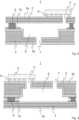
In
In
Die Platine 3 dient hierbei lediglich zum Begrenzen des Raumes, der durch die Ausnehmung 6 entsteht. Die Platinen 2, 3 werden hierbei ebenfalls über Lote bzw. Lot 9, die in beidseitig an jeder der Platine 2, 3 angeordneten Soldermasken 10 aufgetragen werden, aneinander angeordnet bzw. miteinander verbunden.The
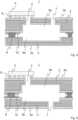
In
In
Fin
Gemäß einer anderen Ausgestaltung des Verfahrensablaufes könnte das Herstellungsverfahren nach dem Bereitstellen (Schritt I), der mechanischen Bearbeitung gemäß Schritte II-IV und der anschließenden Metallisierung (Schritt V) die Schritte Selektives Ätzen, Auftragen der Soldermaske 10 und Finishing der Oberfläche umfassen, bevor dann die Bestückung (z. B. mit dem HF-Bauteil gemäß Schritt VI) und das aneinander Anordnen (gemäß Schritt VII bzw. Schritt VII und Schritt VIII) erfolgt.
According to another embodiment of the process sequence, the production process could include the steps of selective etching, application of the
BezugszeichenlisteReference List
- 11
- Radarsensorradar sensor
- 22
- erste Platinefirst board
- 2a2a
- Metallisierungmetallization
- 33
- Platinecircuit board
- 3a3a
- Metallisierungmetallization
- 44
- HF-BauteilHF component
- 55
- Öffnungopening
- 66
- Ausnehmungrecess
- 6a6a
- Ausnehmungrecess
- 6b6b
- Ausnehmungrecess
- 77
- Öffnungopening
- 88th
- Lotperlesolder bead
- 99
- LotLot
- 1010
- Soldermaskesolder mask
ZITATE ENTHALTEN IN DER BESCHREIBUNGQUOTES INCLUDED IN DESCRIPTION
Diese Liste der vom Anmelder aufgeführten Dokumente wurde automatisiert erzeugt und ist ausschließlich zur besseren Information des Lesers aufgenommen. Die Liste ist nicht Bestandteil der deutschen Patent- bzw. Gebrauchsmusteranmeldung. Das DPMA übernimmt keinerlei Haftung für etwaige Fehler oder Auslassungen.This list of documents cited by the applicant was generated automatically and is included solely for the better information of the reader. The list is not part of the German patent or utility model application. The DPMA assumes no liability for any errors or omissions.
Zitierte PatentliteraturPatent Literature Cited
- DE 102018203106 A1 [0007]DE 102018203106 A1 [0007]
Claims (16)
Translated fromGermanPriority Applications (4)
| Application Number | Priority Date | Filing Date | Title |
|---|---|---|---|
| DE102021214166.8ADE102021214166A1 (en) | 2021-12-10 | 2021-12-10 | Radar sensor and a manufacturing process |
| CN202280077022.0ACN118285019A (en) | 2021-12-10 | 2022-11-14 | Radar sensor and method of manufacture |
| EP22821300.5AEP4445449A1 (en) | 2021-12-10 | 2022-11-14 | Radar sensor and production method |
| PCT/DE2022/200265WO2023104255A1 (en) | 2021-12-10 | 2022-11-14 | Radar sensor and production method |
Applications Claiming Priority (1)
| Application Number | Priority Date | Filing Date | Title |
|---|---|---|---|
| DE102021214166.8ADE102021214166A1 (en) | 2021-12-10 | 2021-12-10 | Radar sensor and a manufacturing process |
Publications (1)
| Publication Number | Publication Date |
|---|---|
| DE102021214166A1true DE102021214166A1 (en) | 2023-06-15 |
Family
ID=84462553
Family Applications (1)
| Application Number | Title | Priority Date | Filing Date |
|---|---|---|---|
| DE102021214166.8APendingDE102021214166A1 (en) | 2021-12-10 | 2021-12-10 | Radar sensor and a manufacturing process |
Country Status (4)
| Country | Link |
|---|---|
| EP (1) | EP4445449A1 (en) |
| CN (1) | CN118285019A (en) |
| DE (1) | DE102021214166A1 (en) |
| WO (1) | WO2023104255A1 (en) |
Cited By (1)
| Publication number | Priority date | Publication date | Assignee | Title |
|---|---|---|---|---|
| DE102023211697A1 (en)* | 2023-11-23 | 2025-05-28 | Continental Autonomous Mobility Germany GmbH | Waveguide arrangement, radar sensor and vehicle |
Families Citing this family (1)
| Publication number | Priority date | Publication date | Assignee | Title |
|---|---|---|---|---|
| CN117693115A (en)* | 2023-07-06 | 2024-03-12 | 荣耀终端有限公司 | Circuit boards and electronic equipment |
Citations (3)
| Publication number | Priority date | Publication date | Assignee | Title |
|---|---|---|---|---|
| DE102014200660A1 (en) | 2014-01-16 | 2015-07-16 | Conti Temic Microelectronic Gmbh | Transmitting and receiving unit for radar signals and method for producing the same |
| DE102018203106A1 (en) | 2018-03-01 | 2019-09-05 | Conti Temic Microelectronic Gmbh | Radar system for detecting the surroundings of a motor vehicle with a plastic antenna |
| DE112013001709B4 (en) | 2012-03-29 | 2020-10-29 | Semiconductor Components Industries, Llc | Electronic semiconductor assembly for millimeter wave semiconductor wafers |
Family Cites Families (4)
| Publication number | Priority date | Publication date | Assignee | Title |
|---|---|---|---|---|
| US9488719B2 (en)* | 2014-05-30 | 2016-11-08 | Toyota Motor Engineering & Manufacturing North America, Inc. | Automotive radar sub-system packaging for robustness |
| DE102016111884B4 (en)* | 2016-06-29 | 2024-08-22 | Infineon Technologies Ag | Apparatus, system and method for automatically testing integrated antennas |
| DE102019200893B4 (en)* | 2019-01-21 | 2023-06-15 | Infineon Technologies Ag | Method of creating a waveguide, circuit device and radar system |
| DE102020113232A1 (en)* | 2020-05-15 | 2021-11-18 | Infineon Technologies Ag | Radio frequency devices and related manufacturing processes |
- 2021
- 2021-12-10DEDE102021214166.8Apatent/DE102021214166A1/enactivePending
- 2022
- 2022-11-14EPEP22821300.5Apatent/EP4445449A1/enactivePending
- 2022-11-14WOPCT/DE2022/200265patent/WO2023104255A1/ennot_activeCeased
- 2022-11-14CNCN202280077022.0Apatent/CN118285019A/enactivePending
Patent Citations (3)
| Publication number | Priority date | Publication date | Assignee | Title |
|---|---|---|---|---|
| DE112013001709B4 (en) | 2012-03-29 | 2020-10-29 | Semiconductor Components Industries, Llc | Electronic semiconductor assembly for millimeter wave semiconductor wafers |
| DE102014200660A1 (en) | 2014-01-16 | 2015-07-16 | Conti Temic Microelectronic Gmbh | Transmitting and receiving unit for radar signals and method for producing the same |
| DE102018203106A1 (en) | 2018-03-01 | 2019-09-05 | Conti Temic Microelectronic Gmbh | Radar system for detecting the surroundings of a motor vehicle with a plastic antenna |
Cited By (1)
| Publication number | Priority date | Publication date | Assignee | Title |
|---|---|---|---|---|
| DE102023211697A1 (en)* | 2023-11-23 | 2025-05-28 | Continental Autonomous Mobility Germany GmbH | Waveguide arrangement, radar sensor and vehicle |
Also Published As
| Publication number | Publication date |
|---|---|
| WO2023104255A1 (en) | 2023-06-15 |
| CN118285019A (en) | 2024-07-02 |
| EP4445449A1 (en) | 2024-10-16 |
Similar Documents
| Publication | Publication Date | Title |
|---|---|---|
| EP3759512B1 (en) | Radar system for detecting the environment of a motor vehicle having a plastic antenna | |
| DE102015108267B4 (en) | Housing for a robust automotive radar subsystem | |
| EP4211748B1 (en) | Radar system for detecting surroundings, comprising a waveguide antenna made of a printed circuit board and a molded part | |
| WO2023104255A1 (en) | Radar sensor and production method | |
| DE102020103778A1 (en) | INVERTED MICROSTRIP TRAVELING WAVE PATCH ARRAY ANTENNA SYSTEM | |
| DE102020103775A1 (en) | Integrated cavity-secured slot array antenna system | |
| DE102020216362A1 (en) | Process for manufacturing a radar sensor | |
| WO2005034288A1 (en) | Device and method for emitting and/or receiving electromagnetic radiation | |
| DE60213057T2 (en) | Mounting arrangement for high-frequency semiconductor device and associated manufacturing method | |
| DE102012203151A1 (en) | SEMICONDUCTOR MODULE WITH INTEGRATED ANTENNA STRUCTURES | |
| DE102015207186A1 (en) | Antenna device for implementing orthogonal antenna characteristics | |
| WO2006061307A1 (en) | Antenna assembly for a radar transceiver | |
| WO2007062971A1 (en) | Antenna array for a radar sensor | |
| DE102018213540B3 (en) | Radar system with a plastic antenna with a predetermined bending point | |
| DE102021209040A1 (en) | Radar system for detecting the surroundings with a waveguide antenna formed from a circuit board and a molded part | |
| DE102021207850A1 (en) | Assortment of radar sensors | |
| DE202020005697U1 (en) | glass pane | |
| DE102024206647B3 (en) | Production process for a radar system for environmental detection with a waveguide antenna formed from several molded parts | |
| EP3966890A1 (en) | Vehicle pane | |
| DE102023211697A1 (en) | Waveguide arrangement, radar sensor and vehicle | |
| DE102018222528A1 (en) | Device for transmitting and / or receiving electromagnetic radiation | |
| DE102016204022A1 (en) | Device for transmitting and / or receiving electromagnetic radiation | |
| DE102023202299A1 (en) | Waveguide antenna, radar sensor and vehicle | |
| DE102020127531A1 (en) | radar sensor | |
| DE102018215459A1 (en) | Radar sensor architecture |
Legal Events
| Date | Code | Title | Description |
|---|---|---|---|
| R081 | Change of applicant/patentee | Owner name:CONTINENTAL AUTONOMOUS MOBILITY GERMANY GMBH, DE Free format text:FORMER OWNER: CONTINENTAL AUTOMOTIVE GMBH, 30165 HANNOVER, DE Owner name:AUMOVIO AUTONOMOUS MOBILITY GERMANY GMBH, DE Free format text:FORMER OWNER: CONTINENTAL AUTOMOTIVE GMBH, 30165 HANNOVER, DE | |
| R163 | Identified publications notified | ||
| R081 | Change of applicant/patentee | Owner name:AUMOVIO AUTONOMOUS MOBILITY GERMANY GMBH, DE Free format text:FORMER OWNER: CONTINENTAL AUTONOMOUS MOBILITY GERMANY GMBH, 85057 INGOLSTADT, DE |