DE102021110607A1 - Device with functional component and plastic housing element and method for verifying the authenticity of such a device - Google Patents
Device with functional component and plastic housing element and method for verifying the authenticity of such a deviceDownload PDFInfo
- Publication number
- DE102021110607A1 DE102021110607A1DE102021110607.9ADE102021110607ADE102021110607A1DE 102021110607 A1DE102021110607 A1DE 102021110607A1DE 102021110607 ADE102021110607 ADE 102021110607ADE 102021110607 A1DE102021110607 A1DE 102021110607A1
- Authority
- DE
- Germany
- Prior art keywords
- plastic housing
- identification
- housing wall
- device identification
- elements
- Prior art date
- Legal status (The legal status is an assumption and is not a legal conclusion. Google has not performed a legal analysis and makes no representation as to the accuracy of the status listed.)
- Pending
Links
Images


Classifications
- G—PHYSICS
- G06—COMPUTING OR CALCULATING; COUNTING
- G06Q—INFORMATION AND COMMUNICATION TECHNOLOGY [ICT] SPECIALLY ADAPTED FOR ADMINISTRATIVE, COMMERCIAL, FINANCIAL, MANAGERIAL OR SUPERVISORY PURPOSES; SYSTEMS OR METHODS SPECIALLY ADAPTED FOR ADMINISTRATIVE, COMMERCIAL, FINANCIAL, MANAGERIAL OR SUPERVISORY PURPOSES, NOT OTHERWISE PROVIDED FOR
- G06Q30/00—Commerce
- G06Q30/018—Certifying business or products
- G06Q30/0185—Product, service or business identity fraud
- G—PHYSICS
- G06—COMPUTING OR CALCULATING; COUNTING
- G06K—GRAPHICAL DATA READING; PRESENTATION OF DATA; RECORD CARRIERS; HANDLING RECORD CARRIERS
- G06K7/00—Methods or arrangements for sensing record carriers, e.g. for reading patterns
- G06K7/10—Methods or arrangements for sensing record carriers, e.g. for reading patterns by electromagnetic radiation, e.g. optical sensing; by corpuscular radiation
- G06K7/14—Methods or arrangements for sensing record carriers, e.g. for reading patterns by electromagnetic radiation, e.g. optical sensing; by corpuscular radiation using light without selection of wavelength, e.g. sensing reflected white light
- G06K7/1404—Methods for optical code recognition
- G—PHYSICS
- G06—COMPUTING OR CALCULATING; COUNTING
- G06K—GRAPHICAL DATA READING; PRESENTATION OF DATA; RECORD CARRIERS; HANDLING RECORD CARRIERS
- G06K19/00—Record carriers for use with machines and with at least a part designed to carry digital markings
- G06K19/06—Record carriers for use with machines and with at least a part designed to carry digital markings characterised by the kind of the digital marking, e.g. shape, nature, code
- G06K19/06009—Record carriers for use with machines and with at least a part designed to carry digital markings characterised by the kind of the digital marking, e.g. shape, nature, code with optically detectable marking
- G06K19/06046—Constructional details
- B—PERFORMING OPERATIONS; TRANSPORTING
- B29—WORKING OF PLASTICS; WORKING OF SUBSTANCES IN A PLASTIC STATE IN GENERAL
- B29C—SHAPING OR JOINING OF PLASTICS; SHAPING OF MATERIAL IN A PLASTIC STATE, NOT OTHERWISE PROVIDED FOR; AFTER-TREATMENT OF THE SHAPED PRODUCTS, e.g. REPAIRING
- B29C45/00—Injection moulding, i.e. forcing the required volume of moulding material through a nozzle into a closed mould; Apparatus therefor
- B29C45/0053—Injection moulding, i.e. forcing the required volume of moulding material through a nozzle into a closed mould; Apparatus therefor combined with a final operation, e.g. shaping
- B—PERFORMING OPERATIONS; TRANSPORTING
- B29—WORKING OF PLASTICS; WORKING OF SUBSTANCES IN A PLASTIC STATE IN GENERAL
- B29C—SHAPING OR JOINING OF PLASTICS; SHAPING OF MATERIAL IN A PLASTIC STATE, NOT OTHERWISE PROVIDED FOR; AFTER-TREATMENT OF THE SHAPED PRODUCTS, e.g. REPAIRING
- B29C45/00—Injection moulding, i.e. forcing the required volume of moulding material through a nozzle into a closed mould; Apparatus therefor
- B29C45/16—Making multilayered or multicoloured articles
- B—PERFORMING OPERATIONS; TRANSPORTING
- B29—WORKING OF PLASTICS; WORKING OF SUBSTANCES IN A PLASTIC STATE IN GENERAL
- B29L—INDEXING SCHEME ASSOCIATED WITH SUBCLASS B29C, RELATING TO PARTICULAR ARTICLES
- B29L2031/00—Other particular articles
- B29L2031/34—Electrical apparatus, e.g. sparking plugs or parts thereof
- B29L2031/3481—Housings or casings incorporating or embedding electric or electronic elements
Landscapes
- Engineering & Computer Science (AREA)
- Physics & Mathematics (AREA)
- General Physics & Mathematics (AREA)
- Theoretical Computer Science (AREA)
- Manufacturing & Machinery (AREA)
- Mechanical Engineering (AREA)
- Business, Economics & Management (AREA)
- Health & Medical Sciences (AREA)
- General Health & Medical Sciences (AREA)
- Toxicology (AREA)
- Artificial Intelligence (AREA)
- Computer Vision & Pattern Recognition (AREA)
- Electromagnetism (AREA)
- Economics (AREA)
- Accounting & Taxation (AREA)
- Development Economics (AREA)
- Entrepreneurship & Innovation (AREA)
- Finance (AREA)
- Marketing (AREA)
- Strategic Management (AREA)
- General Business, Economics & Management (AREA)
- Injection Moulding Of Plastics Or The Like (AREA)
- Investigating Or Analysing Materials By Optical Means (AREA)
- Investigating Or Analysing Materials By The Use Of Chemical Reactions (AREA)
Abstract
Translated fromGerman
Description
Translated fromGermanDie Erfindung betrifft ein Gerät mit einer Funktionskomponente und mit einem Kunststoffgehäuseelement, das zumindest ein Teil eines Gehäuses für die Funktionskomponente ausbildet. Weiterhin betrifft die Erfindung ein Verfahren zur Herstellung eines Kunststoffgehäuseelements für ein solches Gerät, ein Verfahren zur Herstellung eines solchen Geräts und die Verwendung von Geräteidentifizierungselementen zur verwechslungssicheren Identifizierung eines solchen Geräts.The invention relates to a device with a functional component and with a plastic housing element that forms at least part of a housing for the functional component. Furthermore, the invention relates to a method for producing a plastic housing element for such a device, a method for producing such a device and the use of device identification elements for identifying such a device in a way that prevents confusion.
Um die Überprüfung der Echtheit eines Geräts zu ermöglichen und somit Fälschungen von Geräten erkennen zu können, wird techniküblich ein vermeintlich schwer zu fälschender Aufkleber, z.B. ein mit einem Hologramm versehener Aufkleber, auf ein Gehäuse des Geräts aufgeklebt. Weiterhin ist es bekannt, dass Gehäuse mit einer Lasermarkierung zu versehen.In order to enable the authenticity of a device to be checked and thus to be able to identify counterfeit devices, a sticker that is supposedly difficult to counterfeit, e.g. a sticker provided with a hologram, is conventionally affixed to the housing of the device. It is also known to provide the housing with a laser marking.
Es hat sich jedoch in der Praxis gezeigt, dass auch solche Aufkleber oder Lasermarkierungen gefälscht werden.However, it has been shown in practice that such stickers or laser markings are also counterfeited.
Es ist Aufgabe der Erfindung eine verwechslungssichere Identifizierung eines Geräts mit einer Funktionskomponente und mit einem Kunststoffgehäuseelement, das zumindest ein Teil eines Gehäuses für die Funktionskomponente ausbildet, zu ermöglichen.It is the object of the invention to enable identification of a device with a functional component and with a plastic housing element, which forms at least part of a housing for the functional component, so that it cannot be confused.
Diese Aufgabe wird gelöst durch ein Gerät mit einer Funktionskomponente und mit einem Kunststoffgehäuseelement, das zumindest ein Teil eines Gehäuses für die Funktionskomponente ausbildet, wobei das Kunststoffgehäuseelement eine Kunststoffgehäusewand aufweist, wobei die Kunststoffgehäusewand einen in die Kunststoffgehäusewand integrierten und damit einen Bestandteil der Kunststoffgehäusewand ausbildenden Geräteidentifizierungsbereich aufweist, wobei der Geräteidentifizierungsbereich in die Kunststoffgehäusewand integrierte Identifizierungselemente aufweist, wobei diejenigen Identifizierungselemente, die einen Teil einer Oberfläche der Kunststoffgehäusewand ausbilden, Geräteidentifizierungselemente ausbilden, wobei mittels der Geräteidentifizierungselemente der Geräteidentifizierungsbereich für das Gerät individuell ausgebildet ist, so dass das Gerät mittels des Geräteidentifizierungsbereichs verwechslungssicher identifizierbar ist.This object is achieved by a device with a functional component and with a plastic housing element that forms at least part of a housing for the functional component, the plastic housing element having a plastic housing wall, the plastic housing wall having a device identification area integrated into the plastic housing wall and thus forming a part of the plastic housing wall , wherein the device identification area has identification elements integrated into the plastic housing wall, wherein those identification elements that form part of a surface of the plastic housing wall form device identification elements, with the device identification elements being used to design the device identification area for the device individually, so that the device can be identified without confusion by means of the device identification area .
Es erweist sich als vorteilhaft, wenn die Geräteidentifizierungselemente optisch, insbesondere von einem menschlichen Auge und/oder einer Kamera, insbesondere von einer Kamera eines mobilen Kommunikationsgeräts, erkennbar sind, da dann die Geräteidentifizierungselemente besonders leicht erkennbar sind.It has proven to be advantageous if the device identification elements can be recognized optically, in particular by a human eye and/or a camera, in particular by a camera of a mobile communication device, since the device identification elements can then be recognized particularly easily.
Weiterhin erweist es sich als vorteilhaft, wenn das zumindest bei einem Teil der Geräteidentifizierungselemente Bereiche der Geräteidentifizierungselemente aus dem sie jeweilig umgebenden Bereich der übrigen Kunststoffgehäusewand hervorstehen. Hierdurch wird einerseits eine 3-dimensionale Erfassung der Geräteidentifizierungselemente ermöglicht, was die Fälschungssicherheit des Geräteidentifizierungsbereichs erhöht. Weiterhin wird hierdurch das Erkennen eines gefälschten, z.B. eines lediglich aufgedruckten Geräteidentifizierungsbereichs erleichtert, da z.B. ein Zöllner beim Überstreichen der Geräteidentifizierungselemente mit dem Finger eine taktile Rückmeldung erhält.Furthermore, it has proven to be advantageous if, at least in the case of some of the device identification elements, areas of the device identification elements protrude from the area of the rest of the plastic housing wall surrounding them. On the one hand, this enables a 3-dimensional detection of the device identification elements, which increases the protection against forgery of the device identification area. Furthermore, this makes it easier to recognize a forged device identification area, e.g. one that is only printed on, since e.g. a customs officer receives tactile feedback when stroking the device identification elements with his finger.
Weiterhin erweist es sich als vorteilhaft, wenn die Infizierungselemente als im Geräteidentifizierungsbereich, vorzugsweise zufällig, verteilte Partikel ausgebildet sind. Hierdurch kann auf einfache Art und Weise eine sehr hohe Anzahl von unterschiedlichen Geräteidentifizierungsbereichen hergestellt bzw. erzeugt werden.Furthermore, it proves to be advantageous if the infection elements are designed as particles distributed, preferably randomly, in the device identification area. As a result, a very large number of different device identification areas can be produced or generated in a simple manner.
In diesem Zusammenhang erweist es sich als vorteilhaft, wenn mindestens zwei unterschiedliche Ausbildungen von Partikeln vorliegen, wobei die mindestens zwei unterschiedlichen Ausbildungen von Partikeln sich in Form und/oder Größe und/oder Farbe unterscheiden. Hierdurch kann auf besonders einfache Art und Weise eine sehr hohe Anzahl von unterschiedlichen Geräteidentifizierungsbereichen hergestellt bzw. erzeugt werden.In this connection, it proves to be advantageous if at least two different configurations of particles are present, with the at least two different configurations of particles differing in shape and/or size and/or color. As a result, a very large number of different device identification areas can be produced or generated in a particularly simple manner.
Weiterhin erweist es sich als vorteilhaft, wenn die Geräteidentifizierungselemente als unterschiedlich farbige Kunststoffbereiche, die einen Teil der Kunststoffgehäusewand ausbilden und sich vorzugsweise in Form und/oder Größe unterscheiden, ausgebildet sind. Hierdurch kann auf einfache Art und Weise eine sehr hohe Anzahl von unterschiedlichen Geräteidentifizierungsbereichen hergestellt bzw. erzeugt werden.Furthermore, it proves to be advantageous if the device identification elements are designed as differently colored plastic areas which form part of the plastic housing wall and preferably differ in shape and/or size. As a result, a very large number of different device identification areas can be produced or generated in a simple manner.
Ferner erweist es sich als vorteilhaft, wenn das Gerät, insbesondere das Kunststoffgehäuseelement, mit einer Geräteidentifikationszeichenfolge, die insbesondere als Seriennummer des Geräts ausgebildet ist, versehen ist. Durch die zusätzliche Markierung des Geräts mit der Geräteidentifikationszeichenfolge wird in Verbindung mit dem Geräteidentifizierungsbereich die Fälschungssicherheit erhöht.Furthermore, it proves to be advantageous if the device, in particular the plastic housing element, is provided with a device identification character string, which is in particular in the form of a serial number of the device. The additional marking of the device with the device identification character string in conjunction with the device identification area increases counterfeit protection.
Das Gerät kann z.B. ein Leistungshalbleitermodul sein und die Funktionskomponente als Substrat mit Leiterbahnen auf denen Leistungshalbleiterbauelemente angeordnet sind, ausgebildet sein.The device can be a power semiconductor module, for example, and the functional component can be designed as a substrate with conductor tracks on which power semiconductor components are arranged.
Weiterhin wird diese Aufgabe gelöst durch ein Verfahren zur Überprüfung der Echtheit eines erfindungsgemäßen Geräts, mit folgenden Verfahrensschritten:
- a) Empfang von Identifikationsdaten des Geräts, die anhand der Geräteidentifizierungselemente mittels eines Erfassungsgeräts ermittelt wurden,
- b) Ermittlung ob das Gerät eine Fälschung ist anhand eines Vergleichs der Identifikationsdaten mit abgespeicherten Originalidentifikationsdaten von hergestellten Originalgeräten.
- a) receipt of identification data of the device, which was determined using the device identification elements by means of a detection device,
- b) Determining whether the device is a counterfeit based on a comparison of the identification data with stored original identification data from manufactured original devices.
Es erweist sich als vorteilhaft, wenn beim Verfahrensschritt a), falls eine Geräteidentifikationszeichenfolge vorhanden ist, zusätzlich die Geräteidentifikationszeichenfolge empfangen wird, und im Verfahrensschritt b) die Ermittlung ob das Gerät eine Fälschung ist anhand eines Vergleichs der Identifikationsdaten mit Originalidentifikationsdaten von hergestellten Originalgeräten und anhand eines Vergleichs der Geräteidentifikationszeichenfolge mit zu den Originalidentifikationsdaten zugeordneten Originalgeräteidentifikationszeichenfolgen erfolgt. Durch die zusätzliche Markierung des Geräts mit einer Geräteidentifikationszeichenfolge wird in Verbindung mit dem Geräteidentifizierungsbereich die Fälschungssicherheit erhöht.It has proven to be advantageous if, in method step a), if a device identification character sequence is present, the device identification character sequence is also received, and in method step b) the determination of whether the device is a counterfeit based on a comparison of the identification data with original identification data from manufactured original devices and based on a The device identification string is compared with the original device identification strings assigned to the original identification data. The additional marking of the device with a device identification character string in conjunction with the device identification area increases counterfeit security.
Weiterhin erweist es sich als vorteilhaft, wenn bei Verfahrensschritt b) der Vergleich der Identifikationsdaten mit den Originalidentifikationsdaten erfolgt, indem anhand der Identifikationsdaten eine Codierungszeichenfolge ermittelt wird und diese mit aus Originalidentifikationsdaten ermittelten Codierungszeichenfolgen verglichen wird.It is also advantageous if, in method step b), the identification data is compared with the original identification data by using the identification data to determine a coding character sequence and comparing this with coding character sequences determined from the original identification data.
Weiterhin erweist es sich als vorteilhaft, wenn nach Verfahrensschritt b) folgender weiterer Verfahrensschritt durchgeführt wird:
- c) Übermittlung des Ergebnisses, ob das Gerät eine Fälschung ist an das Erfassungsgerät.
- c) Transmission of the result of whether the device is a counterfeit to the detection device.
Weiterhin erweist es sich als vorteilhaft, wenn die Verfahrensschritte a) und b) automatisiert von einer zum Erfassungsgerät 10 nicht zugehörigen Recheneinrichtung durchgeführt werden. Hierdurch kann die Überprüfung der Echtheit eines Geräts besonders rationell durchgeführt werden.Furthermore, it proves to be advantageous if method steps a) and b) are carried out automatically by a computing device that is not associated with the
Weiterhin erweist es sich als vorteilhaft, wenn das Erfassungsgerät oder zumindest ein Teil des Erfassungsgeräts als mobiles Kommunikationsgerät, insbesondere als Smartphone oder Tablet, ausgebildet ist. Ein solches Erfassungsgerät ist überall auf der Welt verbreitet, so dass weltweit Geräte auf deren Echtheit mittels des erfindungsgemäßen Verfahrens auf einfache Art und Weise überprüft werden können.Furthermore, it proves to be advantageous if the detection device or at least a part of the detection device is designed as a mobile communication device, in particular as a smartphone or tablet. Such a detection device is widespread all over the world, so that devices worldwide can be checked for their authenticity in a simple manner using the method according to the invention.
Ferner erweist es sich als vorteilhaft, wenn die Verfahrensschritte a) und b) vom Erfassungsgerät durchgeführt werden. Hierdurch können weltweit Geräte unabhängig von dem Vorhandensein einer Kommunikationsverbindung des Erfassungsgeräts insbesondere mit dem Internet auf deren Echtheit mittels des erfindungsgemäßen Verfahrens auf einfache Art und Weise überprüft werden.Furthermore, it proves to be advantageous if method steps a) and b) are carried out by the detection device. As a result, the authenticity of devices worldwide can be checked in a simple manner using the method according to the invention, regardless of the presence of a communication connection of the detection device, in particular with the Internet.
Weiterhin wird diese Aufgabe gelöst durch ein Verfahren zur Herstellung eines Kunststoffgehäuseelements für ein erfindungsgemäßes Gerät, mit folgendem Verfahrensschritt:
- a) Spritzgießen des Kunststoffgehäuseelements mittels einer Kunststoffspritzgießmaschine, so dass sich eine Kunststoffgehäusewand des Kunststoffgehäuseelements ausbildet, wobei zur Ausbildung eines in die Kunststoffgehäusewand integrierten, einen Bestandteil der Kunststoffgehäusewand ausbildenden Geräteidentifizierungsbereichs, in einem Bereich der Kunststoffgehäusewand Identifizierungselemente mit in die Kunststoffgehäusewand eingespritzt werden, wobei diejenigen Identifizierungselemente, die einen Teil einer Oberfläche der Kunststoffgehäusewand ausbilden, Geräteidentifizierungselemente ausbilden, wobei mittels der Geräteidentifizierungselemente der Geräteidentifizierungsbereich für das Gerät individuell ausgebildet ist, so dass das Gerät mittels des Geräteidentifizierungsbereichs verwechslungssicher identifizierbar ist.
- a) Injection molding of the plastic housing element by means of a plastic injection molding machine, so that a plastic housing wall of the plastic housing element is formed, wherein to form a device identification area that is integrated into the plastic housing wall and forms part of the plastic housing wall, identification elements are also injected into the plastic housing wall in an area of the plastic housing wall, with those identification elements , which form part of a surface of the plastic housing wall, form device identification elements, with the device identification elements being used to form the device identification area for the device individually, so that the device can be identified without confusion by means of the device identification area.
Es erweist sich als vorteilhaft, wenn in einem weiteren nach Verfahrensschritt a) nachfolgenden Verfahrensschritt b) im Geräteidentifizierungsbereich eine Oberflächenschicht abgetragen, insbesondere abgeschliffen, wird. Hierdurch wird die optische Erkennbarkeit der Geräteidentifizierungselemente erleichtert.It has proven to be advantageous if, in a further method step b) following method step a), a surface layer is removed, in particular abraded, in the device identification area. This makes it easier for the device identification elements to be recognized visually.
Weiterhin wird diese Aufgabe gelöst durch ein Verfahren zur Herstellung eines erfindungsgemäßen Geräts, wobei dieses Verfahren das Verfahren zur Herstellung eines Kunststoffgehäuseelements für das Gerät umfasst, mit folgenden nachfolgenden weiteren Verfahrensschritten:
- c) Bereitstellen einer Funktionskomponente,
- d) Anordnen des Kunststoffgehäuseelements und der Funktionskomponente derart zueinander, dass das Kunststoffgehäuseelement, zumindest ein Teil eines Gehäuses für die Funktionskomponente ausbildet.
- c) providing a functional component,
- d) arranging the plastic housing element and the functional component relative to one another in such a way that the plastic housing element forms at least part of a housing for the functional component.
Weiterhin wird diese Aufgabe gelöst durch eine Verwendung von in eine Kunststoffgehäusewand eines Kunststoffgehäuseelements eines erfindungsgemäßen Geräts integrierten Geräteidentifizierungselementen zur verwechslungssicheren Identifizierung des Geräts.Furthermore, this object is achieved by using device identifiers integrated into a plastic housing wall of a plastic housing element of a device according to the invention decorative elements to ensure that the device cannot be mistakenly identified.
Vorteilhafte Ausbildungen des Geräts ergeben sich analog zu vorteilhaften Ausbildungen der Verfahren oder der Verwendung von Geräteidentifizierungselementen zur verwechslungssicheren Identifizierung des Geräts und umgekehrt.Advantageous configurations of the device result analogously to advantageous configurations of the methods or the use of device identification elements for identifying the device in a way that prevents confusion, and vice versa.
Ausführungsbeispiele der Erfindung werden nachfolgend unter Bezugnahme auf die unten stehenden Figuren erläutert. Dabei zeigen:
1 eine perspektivische Ansicht eines erfindungsgemäßen Geräts,2 eine Schnittansicht einer Kunststoffgehäusewand eines erfindungsgemäßen Geräts,3 eine Draufsicht auf eine Ausbildung eines Geräteidentifizierungsbereichs eines erfindungsgemäßen Geräts,4 eine Draufsicht auf eine weitere Ausbildung eines Geräteidentifizierungsbereichs eines erfindungsgemäßen Geräts,5 eine Draufsicht auf eine weitere Ausbildung eines Geräteidentifizierungsbereichs eines erfindungsgemäßen Geräts,6 eine Draufsicht auf eine weitere Ausbildung eines Geräteidentifizierungsbereichs eines erfindungsgemäßen Geräts,7 eine weitere Schnittansicht einer Kunststoffgehäusewand eines erfindungsgemäßen Geräts,8 eine perspektivische Detailansicht eines erfindungsgemäßen Geräts und9 eine Anordnung zur Durchführung eines Verfahrens zur Überprüfung der Echtheit eines erfindungsgemäßen Geräts.
1 a perspective view of a device according to the invention,2 a sectional view of a plastic housing wall of a device according to the invention,3 a plan view of an embodiment of a device identification area of a device according to the invention,4 a plan view of a further embodiment of a device identification area of a device according to the invention,5 a plan view of a further embodiment of a device identification area of a device according to the invention,6 a plan view of a further embodiment of a device identification area of a device according to the invention,7 a further sectional view of a plastic housing wall of a device according to the invention,8th a perspective detailed view of a device according to the invention and9 an arrangement for carrying out a method for checking the authenticity of a device according to the invention.
In
Das erfindungsgemäße Gerät 1 weist eine Funktionskomponente 2 und ein Kunststoffgehäuseelement 3a, das zumindest ein Teil eines Gehäuses 3 für die Funktionskomponente 2 ausbildet, auf, wobei das Kunststoffgehäuseelement 3a eine Kunststoffgehäusewand 3a' aufweist. Im Rahmen der Ausführungsbeispiele ist das Gerät 1 ein Leistungshalbleitermodul und die Funktionskomponente 2 ist als Substrat 2a mit Leiterbahnen auf denen Leistungshalbleiterbauelemente 2b angeordnet und mir den Leiterbahnen elektrisch leitend kontaktiert sind, ausgebildet. Das Substrat 2a kann z.B. als Direct Copper Bonded Substrat (DCB-Substrat), als Active Metal Brazing Substrat (AMB-Substrat) oder als Insulated Metal Substrat (IMS) ausgebildet sein. Das jeweilige Leistungshalbleiterbauelement 2b liegt vorzugsweise in Form eines Leistungshalbleiterschalters oder einer Diode vor. Die Leistungshalbleiterschalter liegen dabei im Allgemeinen in Form von Transistoren, wie z.B. IGBTs (Insulated Gate Bipolar Transistor) oder MOSFETs (Metal Oxide Semiconductor Field Effect Transistor), oder in Form von Thyristoren vor. Das Substrat 2a ist vorzugsweise auf einer Grundplatte 7 des Leistungshalbleitermoduls angeordnet. Die Leistungshalbleiterbauelemente 2b sind vorzugsweise zu einer Halbbrückenschaltung miteinander elektrisch verschaltet. Das Leistungshalbleitermodul weist bei den Ausführungsbeispielen weiterhin elektrische Laststromanschlüsse 20 und vorzugsweise Steueranschlüsse 21 zur Ansteuerung von Leistungshalbleiterschaltern des Leistungshalbleitermoduls auf.The
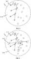
Die Kunststoffgehäusewand 3a' weist einen in die Kunststoffgehäusewand 3a' integrierten und damit einen Bestandteil der Kunststoffgehäusewand 3a' ausbildenden Geräteidentifizierungsbereich 4 auf. Der Geräteidentifizierungsbereich 4 weist in die Kunststoffgehäusewand 3a' integrierte Identifizierungselemente 5 auf, wobei diejenigen Identifizierungselemente 5, die einen Teil einer Oberfläche 3a'' der Kunststoffgehäusewand 3a' ausbilden, Geräteidentifizierungselemente 5a ausbilden (siehe
Die Geräteidentifizierungselemente 5a sind vorzugsweise optisch, insbesondere von einem menschlichen Auge und/oder einer Kamera, insbesondere von einer Kamera eines mobilen Kommunikationsgeräts, erkennbar. Die Geräteidentifizierungselemente 5a weisen hierzu eine ausreichende Größe auf.The
Wie bespielhaft in
Die Infizierungselemente 5 sind, wie beispielhaft in den
Wie beispielhaft in
Alternativ können die Geräteidentifizierungselemente 5a, wie beispielhaft in
Das Gerät 1, insbesondere das Kunststoffgehäuseelement 3a, ist vorzugsweise mit einer Geräteidentifikationszeichenfolge 6, die insbesondere als Seriennummer des Geräts 1 ausgebildet ist, versehen. Durch die zusätzliche Markierung des Geräts 1 mit der Geräteidentifikationszeichenfolge 6 wird in Verbindung mit dem Geräteidentifizierungsbereich 4 die Fälschungssicherheit erhöht.The
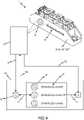
Im Folgenden wird ein Verfahren zur Überprüfung der Echtheit des Geräts 1 beschrieben.
In einem Verfahrensschritt a) erfolgt ein Empfang 9 von Identifikationsdaten 8 des Geräts 1, die anhand der Geräteidentifizierungselemente 4 mittels eines Erfassungsgeräts 10 ermittelt wurden. Das Erfassungsgerät 10 oder zumindest ein Teil des Erfassungsgeräts 10 ist vorzugsweise als mobiles Kommunikationsgerät, insbesondere als Smartphone oder Tablet ausgebildet. Zur Ermittlung der Identifikationsdaten 8 wird der Geräteidentifizierungsbereich 4 vom Erfassungsgerät 10 vorzugsweise abfotografiert. Anschließend wird das Foto, genauer ausgedrückt, die betreffende Fotodatei, vorzugsweise vom Erfassungsgerät 10, an eine Recheneinrichtung 15, z.B. mittels einer auf dem Erfassungsgerät 15 ablaufenden App oder z.B. mittels einer E-Mail, übermittelt. Im Rahmen des Ausführungsbeispiels werden die Identifikationsdaten 8 von einer nicht zum Erfassungsgerät 10 zugehörigen Recheneinrichtung 15 empfangen, was in
In einem nachfolgenden Verfahrensschritt b) erfolgt eine Ermittlung ob das Gerät 1 eine Fälschung ist anhand eines Vergleichs 11 der Identifikationsdaten 8 mit abgespeicherten Originalidentifikationsdaten 8' von hergestellten Originalgeräten. Zur Erstellung der Originalidentifikationsdaten 8' werden dieIn a subsequent method step b), a determination is made as to whether the
Geräteidentifizierungsbereiche 4 von Originalgeräten bzw. von Originalkunststoffgehäuseelementen abfotografiert und die entsprechenden Fotos als Originalidentifikationsdaten 8' abgespeichert. Im einfachsten Fall wird der Vergleich 11 der Identifikationsdaten 8 mit abgespeicherten Originalidentifikationsdaten 8' von einem Menschen durch visuellen Vergleich der Identifikationsdaten 8 mit abgespeicherten Originalidentifikationsdaten 8' an einem Bildschirm durchgeführt. Vorzugsweise werden die Verfahrensschritte a) und b) automatisiert von der zum Erfassungsgerät 10 nicht zugehörigen Recheneinrichtung 15, z.B. von einem Server, einem PC bzw. von einer Rechenanlage, durchgeführt. Bei Verfahrensschritt b) erfolgt der Vergleich 11 der Identifikationsdaten 8 mit den Originalidentifikationsdaten 8' vorzugsweise, indem anhand der Identifikationsdaten 8 eine Codierungszeichenfolge ermittelt wird und diese mit aus Originalidentifikationsdaten 8' ermittelten Codierungszeichenfolgen verglichen wird. Das Ermitteln einer Codierungszeichenfolge anhand der Identifikationsdaten 8 kann, wie bespielhaft in den
Das Ermitteln einer Codierungszeichenfolge, anhand der Identifikationsdaten 8, kann aber auch vorab auf einer anderen Einrichtung, insbesondere auf dem Erfassungsgerät 10 erfolgen und diese dann als Identifikationsdaten 8, insbesondere an die Recheneinrichtung 15 übermittelt werden. In diesem Fall werden im Verfahrensschritt a) die Codierungszeichenfolge als Identifikationsdaten 8 des Geräts 1 empfangen. Im Sinne der Erfindung können sowohl die Identifikationsdaten 8 als auch die Originalidentifikationsdaten 8' auch bereits in Form einer Codierungszeichenfolge vorliegen.However, a coding character sequence can also be determined using the
Beim Verfahrensschritt a) wird vorzugsweise, falls vorhanden, zusätzlich die Geräteidentifikationszeichenfolge 6 empfangen, was in
In einem nach dem Verfahrensschritt b) vorzugsweise nachfolgenden Verfahrensschritt c) erfolgt eine Übermittlung des Ergebnisses, ob das Gerät 1 eine Fälschung ist an das Erfassungsgerät 10, was in
Es sei angemerkt, dass die Verfahrensschritte a) und b) auch vom Erfassungsgerät 10 durchgeführt werden können, wobei in diesem Fall beim Verfahrensschritt a) der Empfang von Identifikationsdaten des Geräts 1 von einer im Erfassungsgerät 10 integrierten Recheneinrichtung erfolgt.It should be noted that the method steps a) and b) can also be carried out by the
Im Folgenden wird ein Verfahren zur Herstellung eines Kunststoffgehäuseelements 3a für das Gerät 1 beschrieben.A method for producing a
In einem Verfahrensschritt a) erfolgt ein Spritzgießen des Kunststoffgehäuseelements 3a mittels einer Kunststoffspritzgießmaschine, so dass sich eine Kunststoffgehäusewand 3a' des Kunststoffgehäuseelements 3a ausbildet. Zur Ausbildung eines in die Kunststoffgehäusewand 3a' integrierten, einen Bestandteil der Kunststoffgehäusewand 3a' ausbildenden Geräteidentifizierungsbereichs 4, in einem Bereich der Kunststoffgehäusewand 3a', werden Identifizierungselemente 5 mit in die Kunststoffgehäusewand 3a' eingespritzt, wobei diejenigen Identifizierungselemente 5, die einen Teil einer Oberfläche 3a'' der Kunststoffgehäusewand 3a' ausbilden, Geräteidentifizierungselemente 5a' ausbilden. Mittels der Geräteidentifizierungselemente 5a' ist der Geräteidentifizierungsbereich 4 für das Gerät 1 individuell ausgebildet ist, so dass das Gerät 1 mittels des Geräteidentifizierungsbereichs 4 verwechslungssicher identifizierbar ist. Das Spritzgießen des Kunststoffgehäuseelements 3a erfolgt vorzugsweise mittels Mehrkomponenten-Spritzgießverfahren, insbesondere z.B. mittels Kernrückzugstechnik, Sandwich-Verfahren, Koinjektion oder Marmorierung.In a method step a), the
Der Kunststoff aus dem die Kunststoffgehäusewand 3a' im Geräteidentifizierungsbereich 4 ausgebildet ist und in dem die Identifizierungselemente 5 integriert sind, ist vorzugsweise der gleiche Kunststoff, wie der Kunststoff aus dem die übrige Kunststoffgehäusewand 3a' ausgebildet ist.The plastic from which the
In einem optional nachfolgenden Verfahrensschritt b) kann im Geräteidentifizierungsbereich 4 eine Oberflächenschicht abgetragen, insbesondere abgeschliffen, werden.In an optionally subsequent method step b), a surface layer can be removed, in particular ground off, in the
Im Folgenden wird ein Verfahren zur Herstellung des Geräts 1 beschreiben, wobei dieses Verfahren, das oben beschriebene Verfahren zur Herstellung des Kunststoffgehäuseelements 3a umfasst.A method for manufacturing the
In einem nachfolgenden weiteren Verfahrensschritt c) erfolgt ein Bereitstellen der Funktionskomponente 2.In a subsequent further method step c), the
In einem nachfolgenden weiteren Verfahrensschritt d) erfolgt ein Anordnen des Kunststoffgehäuseelements 3a und der Funktionskomponente 2 derart zueinander, dass das Kunststoffgehäuseelement 3a, zumindest ein Teil eines Gehäuses 3 für die Funktionskomponente 2 ausbildet.In a subsequent further method step d), the
Die Erfindung verwendet in die Kunststoffgehäusewand 3a' des Kunststoffgehäuseelements 3a des Geräts 1 integrierte Geräteidentifizierungselemente 5a zur verwechslungssicheren Identifizierung des Geräts 1.The invention uses
Claims (19)
Translated fromGermanPriority Applications (3)
| Application Number | Priority Date | Filing Date | Title |
|---|---|---|---|
| DE102021110607.9ADE102021110607A1 (en) | 2021-04-26 | 2021-04-26 | Device with functional component and plastic housing element and method for verifying the authenticity of such a device |
| US17/716,268US11995508B2 (en) | 2021-04-26 | 2022-04-08 | Device having functional component and a plastic housing element, and method for verifying the authenticity of such a device |
| CN202210430316.9ACN115330402A (en) | 2021-04-26 | 2022-04-22 | Device with functional component and plastic housing element and method for verifying the authenticity thereof |
Applications Claiming Priority (1)
| Application Number | Priority Date | Filing Date | Title |
|---|---|---|---|
| DE102021110607.9ADE102021110607A1 (en) | 2021-04-26 | 2021-04-26 | Device with functional component and plastic housing element and method for verifying the authenticity of such a device |
Publications (1)
| Publication Number | Publication Date |
|---|---|
| DE102021110607A1true DE102021110607A1 (en) | 2022-10-27 |
Family
ID=83508247
Family Applications (1)
| Application Number | Title | Priority Date | Filing Date |
|---|---|---|---|
| DE102021110607.9APendingDE102021110607A1 (en) | 2021-04-26 | 2021-04-26 | Device with functional component and plastic housing element and method for verifying the authenticity of such a device |
Country Status (3)
| Country | Link |
|---|---|
| US (1) | US11995508B2 (en) |
| CN (1) | CN115330402A (en) |
| DE (1) | DE102021110607A1 (en) |
Families Citing this family (1)
| Publication number | Priority date | Publication date | Assignee | Title |
|---|---|---|---|---|
| DE102021110607A1 (en)* | 2021-04-26 | 2022-10-27 | Semikron Elektronik Gmbh & Co. Kg | Device with functional component and plastic housing element and method for verifying the authenticity of such a device |
Citations (2)
| Publication number | Priority date | Publication date | Assignee | Title |
|---|---|---|---|---|
| US20060086791A1 (en) | 2004-10-27 | 2006-04-27 | Symbol Technologies, Inc. | Method of identifying and authenticating products using an identification pattern and a bar code reader |
| DE102019201529A1 (en) | 2019-02-06 | 2020-08-06 | Hahn-Schickard-Gesellschaft für angewandte Forschung e.V. | Control device for a manufacturing plant, tracking device, manufacturing data determiner, methods and computer program |
Family Cites Families (43)
| Publication number | Priority date | Publication date | Assignee | Title |
|---|---|---|---|---|
| FR2738971B1 (en)* | 1995-09-19 | 1997-10-10 | Schlumberger Ind Sa | METHOD FOR DETERMINING AN ENCRYPTION KEY ASSOCIATED WITH AN INTEGRATED CIRCUIT |
| US7466556B2 (en)* | 1999-08-04 | 2008-12-16 | Super Talent Electronics, Inc. | Single chip USB packages with swivel cover |
| WO2001043086A1 (en)* | 1999-12-08 | 2001-06-14 | Mischenko Valentin Alexandrovi | Method and system for authentication of articles |
| US7005733B2 (en)* | 1999-12-30 | 2006-02-28 | Koemmerling Oliver | Anti tamper encapsulation for an integrated circuit |
| EP1168253A1 (en)* | 2000-06-28 | 2002-01-02 | Sicpa Holding S.A. | Use of communication equipment and method for authenticating an item, specifically documents, in particular security documents, communication equipment for authenticating items, and items to be authenticated by communication equipment |
| US6632654B1 (en)* | 2001-08-08 | 2003-10-14 | Dade Microscan Inc. | Canister for inventorying susceptability test devices in an automated microbiological analyzer |
| DE10145468C1 (en)* | 2001-09-14 | 2003-01-16 | Infineon Technologies Ag | Process for fixing a semiconductor device on a switching device, used in flip-chip technology, comprises preparing a semiconductor device with bond pads on one surface |
| DE10325564B4 (en)* | 2003-06-05 | 2008-12-18 | Infineon Technologies Ag | Smart card module |
| US20050064435A1 (en)* | 2003-09-24 | 2005-03-24 | Xing Su | Programmable molecular barcodes |
| DE10351129B4 (en)* | 2003-11-03 | 2008-12-24 | Ovd Kinegram Ag | Diffractive security element with a halftone image |
| US8102657B2 (en)* | 2003-12-02 | 2012-01-24 | Super Talent Electronics, Inc. | Single shot molding method for COB USB/EUSB devices with contact pad ribs |
| US7872873B2 (en)* | 2003-12-02 | 2011-01-18 | Super Talent Electronics, Inc. | Extended COB-USB with dual-personality contacts |
| US20050140497A1 (en)* | 2003-12-30 | 2005-06-30 | Entrust Limited | Method and apparatus for securely providing identification information using translucent identification member with filter |
| EP1851732A4 (en)* | 2005-01-19 | 2010-08-04 | Agency Science Tech & Res | IDENTIFICATION LABEL, OBJECT ADAPTED TO BE IDENTIFIED AND RELATED METHODS, DEVICES AND SYSTEMS |
| US8874477B2 (en)* | 2005-10-04 | 2014-10-28 | Steven Mark Hoffberg | Multifactorial optimization system and method |
| US7630559B2 (en)* | 2005-11-21 | 2009-12-08 | Fuji Xerox Co., Ltd. | Confirmation system for authenticity of article and confirmation method |
| US20090218401A1 (en)* | 2006-05-11 | 2009-09-03 | Singular Id Pte Ltd | Method of identifying an object, an identification tag, an object adapted to be identified, and related device and system |
| CA2684789A1 (en)* | 2007-04-24 | 2008-10-30 | Sicpa Holding Sa | Method of marking a document or item; method and device for identifying the marked document or item; use of circular polarizing particles |
| EP1990212A1 (en)* | 2007-05-07 | 2008-11-12 | CSEM Centre Suisse d'Electronique et de Microtechnique SA Recherche et Développement | Unique security device for the identification or authentication of valuable goods, fabrication process and method for securing valuable goods using such a unique security device |
| DE102008032781A1 (en)* | 2008-07-11 | 2010-01-21 | Klöckner Pentaplast GmbH & Co. KG | Packaging film for product authentication, authentication method and system |
| US20110312078A1 (en)* | 2010-06-17 | 2011-12-22 | Geneasys Pty Ltd | Microfluidic device for detecting target nucleic acid sequences in mitochondrial dna |
| US20130232830A1 (en)* | 2011-12-08 | 2013-09-12 | Rebekah P. Barisic | Method and apparatus for identifying a work object |
| US10543704B2 (en)* | 2012-11-01 | 2020-01-28 | Owens-Brockway Glass Container Inc. | Particle-coded container |
| US20140138839A1 (en)* | 2012-11-20 | 2014-05-22 | Samsung Electro-Mechanics Co., Ltd. | Power semiconductor module |
| MX2015007822A (en)* | 2012-12-20 | 2015-08-20 | Sicpa Holding Sa | Chiral liquid crystal polymer layer or pattern comprising randomly distributed craters therein. |
| US8888005B2 (en)* | 2013-04-12 | 2014-11-18 | David Prokop | Uniquely identifiable drug dosage form units |
| US9681558B2 (en)* | 2014-08-12 | 2017-06-13 | Infineon Technologies Ag | Module with integrated power electronic circuitry and logic circuitry |
| US11198122B2 (en)* | 2015-07-17 | 2021-12-14 | Axxin Pty Ltd | Diagnostic test assembly, apparatus, method |
| EP3168825A1 (en)* | 2015-11-10 | 2017-05-17 | Alcatel Lucent | A unique identifier module, a system for providing with a unique identification, a related module and related method |
| US10217577B2 (en)* | 2017-04-03 | 2019-02-26 | Roku, Inc. | Remote control with configurable buttons |
| CA3075303A1 (en)* | 2017-09-09 | 2019-03-14 | The Broad Institute, Inc. | Multi-effector crispr based diagnostic systems |
| US11423632B2 (en)* | 2017-10-24 | 2022-08-23 | Nec Corporation | Device and method for determining surface irregularities with irradiation angle |
| US20190139909A1 (en)* | 2017-11-09 | 2019-05-09 | Lexmark International, Inc. | Physical Unclonable Functions in Integrated Circuit Chip Packaging for Security |
| WO2019134431A1 (en)* | 2018-01-02 | 2019-07-11 | 海南亚元防伪技术研究所(普通合伙) | Anti-counterfeit method employing hand-tearing of textured portion and product and material thereof |
| WO2020212031A1 (en)* | 2019-04-18 | 2020-10-22 | Abb Power Grids Switzerland Ag | Power semiconductor module with laser-welded leadframe |
| GB2587223B (en)* | 2019-09-19 | 2023-07-19 | Pragmatic Printing Ltd | Electronic device and associated method of manufacture |
| WO2021076972A1 (en)* | 2019-10-17 | 2021-04-22 | C2Sense, Inc. | Luminescence imaging for sensing |
| DE102020115831B4 (en)* | 2020-06-16 | 2024-03-14 | Semikron Elektronik Gmbh & Co. Kg | Power electronic switching device with a printing device |
| US11548309B2 (en)* | 2020-06-29 | 2023-01-10 | Gideon Samid | Doqumint technology: counterfeit resistant documentation |
| DE102021110607A1 (en)* | 2021-04-26 | 2022-10-27 | Semikron Elektronik Gmbh & Co. Kg | Device with functional component and plastic housing element and method for verifying the authenticity of such a device |
| US12014963B2 (en)* | 2021-06-29 | 2024-06-18 | Infineon Technologies Ag | Power semiconductor module having protrusions as fixing structures |
| DE102021121797A1 (en)* | 2021-08-23 | 2023-02-23 | Infineon Technologies Ag | POWER SEMICONDUCTOR MODULE WITH SOCKET OR PRESS-FIT PIN AND METHOD OF ITS MANUFACTURE |
| US12068226B2 (en)* | 2021-09-13 | 2024-08-20 | Infineon Technologies Ag | Semiconductor assembly with multi-device cooling |
- 2021
- 2021-04-26DEDE102021110607.9Apatent/DE102021110607A1/enactivePending
- 2022
- 2022-04-08USUS17/716,268patent/US11995508B2/enactiveActive
- 2022-04-22CNCN202210430316.9Apatent/CN115330402A/enactivePending
Patent Citations (2)
| Publication number | Priority date | Publication date | Assignee | Title |
|---|---|---|---|---|
| US20060086791A1 (en) | 2004-10-27 | 2006-04-27 | Symbol Technologies, Inc. | Method of identifying and authenticating products using an identification pattern and a bar code reader |
| DE102019201529A1 (en) | 2019-02-06 | 2020-08-06 | Hahn-Schickard-Gesellschaft für angewandte Forschung e.V. | Control device for a manufacturing plant, tracking device, manufacturing data determiner, methods and computer program |
Also Published As
| Publication number | Publication date |
|---|---|
| US20220343091A1 (en) | 2022-10-27 |
| US11995508B2 (en) | 2024-05-28 |
| CN115330402A (en) | 2022-11-11 |
Similar Documents
| Publication | Publication Date | Title |
|---|---|---|
| DE68927201T2 (en) | Security fence | |
| DE60221037T2 (en) | METHOD AND SYSTEM FOR RELEASING A SLOT MODULE | |
| DE102014109278A1 (en) | Charging system with a circuit for delaying the power supply | |
| DE1931536A1 (en) | Process for the production and identification of documents, documents produced by this process and device for identifying the documents produced by the process | |
| DE102004015283A1 (en) | Card IC | |
| DE19731983A1 (en) | Contactlessly operated data carrier | |
| DE102021110607A1 (en) | Device with functional component and plastic housing element and method for verifying the authenticity of such a device | |
| EP2387798B1 (en) | Method for verifying an identification circuit | |
| DE10393637T5 (en) | Electrical adapter for the protection of electrical interfaces | |
| DE10325564B4 (en) | Smart card module | |
| EP1079672A3 (en) | Plastic article comprising electrical contacts | |
| DE102020134849A1 (en) | VEHICLE INTERIOR FAIRING PART WITH INTEGRATED ELECTRONICS AND METHOD OF MANUFACTURING | |
| DE102019127249A1 (en) | DEVICE AND METHOD FOR DETECTING ION WALK | |
| DE102007038318A1 (en) | Embossed card-shaped data carrier | |
| DE102018113571A1 (en) | Method for producing a metal-ceramic substrate and metal-ceramic substrate | |
| DE102018209818B4 (en) | Method for producing a value or security document blank with an electronic circuit, a value or security document blank and a security and value document | |
| DE602004005605T2 (en) | MECHANISM FOR LOCKING AN ELECTRONIC ASSEMBLY | |
| DE102010022360A1 (en) | Method for controlling access to e.g. company premises, involves testing input codes by utilizing testing device, and granting clearance when input codes comprise specific characters of release codes | |
| EP3089118B1 (en) | Access authorization system comprising at least one assembly of a plurality of microparticles and at least one identifying unit | |
| EP1911334B1 (en) | Method and system for electrically coupling an information carrier to a contact element | |
| DE112019007005T5 (en) | Keypad for secure data entry | |
| DE102019002160A1 (en) | Security insert with a tactile lacquer arrangement for an identity document and method for producing such a security insert | |
| DE102018221841A1 (en) | Illuminated display device | |
| DE102013214478A1 (en) | Multiple circuit board benefit and method of making the same | |
| EP2722789A2 (en) | Method for verifying the authenticity of a portable data carrier |
Legal Events
| Date | Code | Title | Description |
|---|---|---|---|
| R012 | Request for examination validly filed | ||
| R016 | Response to examination communication |