DE102019109137A1 - COMPONENT FOR A DISPLAY DEVICE, DISPLAY DEVICE AND METHOD OF OPERATING THE DISPLAY DEVICE - Google Patents
COMPONENT FOR A DISPLAY DEVICE, DISPLAY DEVICE AND METHOD OF OPERATING THE DISPLAY DEVICEDownload PDFInfo
- Publication number
- DE102019109137A1 DE102019109137A1DE102019109137.3ADE102019109137ADE102019109137A1DE 102019109137 A1DE102019109137 A1DE 102019109137A1DE 102019109137 ADE102019109137 ADE 102019109137ADE 102019109137 A1DE102019109137 A1DE 102019109137A1
- Authority
- DE
- Germany
- Prior art keywords
- led chip
- display device
- row
- pixel
- led
- Prior art date
- Legal status (The legal status is an assumption and is not a legal conclusion. Google has not performed a legal analysis and makes no representation as to the accuracy of the status listed.)
- Pending
Links
Images


Classifications
- G—PHYSICS
- G09—EDUCATION; CRYPTOGRAPHY; DISPLAY; ADVERTISING; SEALS
- G09G—ARRANGEMENTS OR CIRCUITS FOR CONTROL OF INDICATING DEVICES USING STATIC MEANS TO PRESENT VARIABLE INFORMATION
- G09G3/00—Control arrangements or circuits, of interest only in connection with visual indicators other than cathode-ray tubes
- G09G3/20—Control arrangements or circuits, of interest only in connection with visual indicators other than cathode-ray tubes for presentation of an assembly of a number of characters, e.g. a page, by composing the assembly by combination of individual elements arranged in a matrix no fixed position being assigned to or needed to be assigned to the individual characters or partial characters
- G09G3/22—Control arrangements or circuits, of interest only in connection with visual indicators other than cathode-ray tubes for presentation of an assembly of a number of characters, e.g. a page, by composing the assembly by combination of individual elements arranged in a matrix no fixed position being assigned to or needed to be assigned to the individual characters or partial characters using controlled light sources
- G09G3/30—Control arrangements or circuits, of interest only in connection with visual indicators other than cathode-ray tubes for presentation of an assembly of a number of characters, e.g. a page, by composing the assembly by combination of individual elements arranged in a matrix no fixed position being assigned to or needed to be assigned to the individual characters or partial characters using controlled light sources using electroluminescent panels
- G09G3/32—Control arrangements or circuits, of interest only in connection with visual indicators other than cathode-ray tubes for presentation of an assembly of a number of characters, e.g. a page, by composing the assembly by combination of individual elements arranged in a matrix no fixed position being assigned to or needed to be assigned to the individual characters or partial characters using controlled light sources using electroluminescent panels semiconductive, e.g. using light-emitting diodes [LED]
- G09G3/3208—Control arrangements or circuits, of interest only in connection with visual indicators other than cathode-ray tubes for presentation of an assembly of a number of characters, e.g. a page, by composing the assembly by combination of individual elements arranged in a matrix no fixed position being assigned to or needed to be assigned to the individual characters or partial characters using controlled light sources using electroluminescent panels semiconductive, e.g. using light-emitting diodes [LED] organic, e.g. using organic light-emitting diodes [OLED]
- G09G3/3216—Control arrangements or circuits, of interest only in connection with visual indicators other than cathode-ray tubes for presentation of an assembly of a number of characters, e.g. a page, by composing the assembly by combination of individual elements arranged in a matrix no fixed position being assigned to or needed to be assigned to the individual characters or partial characters using controlled light sources using electroluminescent panels semiconductive, e.g. using light-emitting diodes [LED] organic, e.g. using organic light-emitting diodes [OLED] using a passive matrix
- G—PHYSICS
- G06—COMPUTING OR CALCULATING; COUNTING
- G06F—ELECTRIC DIGITAL DATA PROCESSING
- G06F3/00—Input arrangements for transferring data to be processed into a form capable of being handled by the computer; Output arrangements for transferring data from processing unit to output unit, e.g. interface arrangements
- G06F3/14—Digital output to display device ; Cooperation and interconnection of the display device with other functional units
- G06F3/1423—Digital output to display device ; Cooperation and interconnection of the display device with other functional units controlling a plurality of local displays, e.g. CRT and flat panel display
- G06F3/1446—Digital output to display device ; Cooperation and interconnection of the display device with other functional units controlling a plurality of local displays, e.g. CRT and flat panel display display composed of modules, e.g. video walls
- G—PHYSICS
- G09—EDUCATION; CRYPTOGRAPHY; DISPLAY; ADVERTISING; SEALS
- G09G—ARRANGEMENTS OR CIRCUITS FOR CONTROL OF INDICATING DEVICES USING STATIC MEANS TO PRESENT VARIABLE INFORMATION
- G09G3/00—Control arrangements or circuits, of interest only in connection with visual indicators other than cathode-ray tubes
- G09G3/006—Electronic inspection or testing of displays and display drivers, e.g. of LED or LCD displays
- G—PHYSICS
- G09—EDUCATION; CRYPTOGRAPHY; DISPLAY; ADVERTISING; SEALS
- G09G—ARRANGEMENTS OR CIRCUITS FOR CONTROL OF INDICATING DEVICES USING STATIC MEANS TO PRESENT VARIABLE INFORMATION
- G09G2300/00—Aspects of the constitution of display devices
- G09G2300/02—Composition of display devices
- G09G2300/026—Video wall, i.e. juxtaposition of a plurality of screens to create a display screen of bigger dimensions
- G—PHYSICS
- G09—EDUCATION; CRYPTOGRAPHY; DISPLAY; ADVERTISING; SEALS
- G09G—ARRANGEMENTS OR CIRCUITS FOR CONTROL OF INDICATING DEVICES USING STATIC MEANS TO PRESENT VARIABLE INFORMATION
- G09G2300/00—Aspects of the constitution of display devices
- G09G2300/04—Structural and physical details of display devices
- G09G2300/0439—Pixel structures
- G09G2300/0452—Details of colour pixel setup, e.g. pixel composed of a red, a blue and two green components
- G—PHYSICS
- G09—EDUCATION; CRYPTOGRAPHY; DISPLAY; ADVERTISING; SEALS
- G09G—ARRANGEMENTS OR CIRCUITS FOR CONTROL OF INDICATING DEVICES USING STATIC MEANS TO PRESENT VARIABLE INFORMATION
- G09G2310/00—Command of the display device
- G09G2310/02—Addressing, scanning or driving the display screen or processing steps related thereto
- G09G2310/0264—Details of driving circuits
- G09G2310/0297—Special arrangements with multiplexing or demultiplexing of display data in the drivers for data electrodes, in a pre-processing circuitry delivering display data to said drivers or in the matrix panel, e.g. multiplexing plural data signals to one D/A converter or demultiplexing the D/A converter output to multiple columns
- G—PHYSICS
- G09—EDUCATION; CRYPTOGRAPHY; DISPLAY; ADVERTISING; SEALS
- G09G—ARRANGEMENTS OR CIRCUITS FOR CONTROL OF INDICATING DEVICES USING STATIC MEANS TO PRESENT VARIABLE INFORMATION
- G09G2330/00—Aspects of power supply; Aspects of display protection and defect management
- G09G2330/08—Fault-tolerant or redundant circuits, or circuits in which repair of defects is prepared
- G—PHYSICS
- G09—EDUCATION; CRYPTOGRAPHY; DISPLAY; ADVERTISING; SEALS
- G09G—ARRANGEMENTS OR CIRCUITS FOR CONTROL OF INDICATING DEVICES USING STATIC MEANS TO PRESENT VARIABLE INFORMATION
- G09G2330/00—Aspects of power supply; Aspects of display protection and defect management
- G09G2330/10—Dealing with defective pixels
Landscapes
- Engineering & Computer Science (AREA)
- Theoretical Computer Science (AREA)
- Physics & Mathematics (AREA)
- General Physics & Mathematics (AREA)
- Computer Hardware Design (AREA)
- Multimedia (AREA)
- Human Computer Interaction (AREA)
- General Engineering & Computer Science (AREA)
- Led Device Packages (AREA)
- Devices For Indicating Variable Information By Combining Individual Elements (AREA)
- Control Of Indicators Other Than Cathode Ray Tubes (AREA)
- Control Of El Displays (AREA)
Abstract
Translated fromGermanDescription
Translated fromGermanDie Erfindung betrifft ein Bauelement für eine Anzeigevorrichtung sowie eine Anzeigevorrichtung und ein Verfahren zum Betreiben der Anzeigevorrichtung. Darüber hinaus werden ein Computerprogramm zum Betreiben der Anzeigevorrichtung und ein computerlesbares Speichermedium angegeben.The invention relates to a component for a display device as well as a display device and a method for operating the display device. In addition, a computer program for operating the display device and a computer-readable storage medium are specified.
Anzeigevorrichtungen wie Videowände (engl. „video wall“) können zur Darstellung einzelner Bildelemente (Pixel, engl. „picture element“) aus diskreten LEDs aufgebaut sein (sogenannte „LED wall“).Display devices such as video walls can be constructed from discrete LEDs (so-called “LED wall”) to display individual picture elements (pixels).
Die Aufgabe, die der Erfindung zugrunde liegt, ist es, ein Bauelement für eine solche Anzeigevorrichtung sowie eine Anzeigevorrichtung und ein Verfahren zum Betreiben derselben anzugeben, das eine einfache Herstellung der Anzeigevorrichtung erlaubt und beiträgt, die Kosten der Herstellung gering zu halten.The object on which the invention is based is to provide a component for such a display device, as well as a display device and a method for operating the same, which allows simple production of the display device and helps to keep production costs low.
Die Aufgabe wird gelöst durch die unabhängigen Patentansprüche. Vorteilhafte Ausgestaltungen sind in den Unteransprüchen gekennzeichnet.The object is achieved by the independent patent claims. Advantageous configurations are characterized in the subclaims.
Gemäß einem ersten Aspekt der Erfindung wird ein Bauelement für eine Anzeigevorrichtung angegeben.According to a first aspect of the invention, a component for a display device is specified.
Bei dem Bauelement handelt es sich beispielsweise um ein oberflächenmontierbares Bauelement (SMD, „surface-mounted device“) auf einer Leiterplatte (PCB, „printed circuit board“). Insbesondere mehrere solcher Bauelemente können horizontal und/oder vertikal nebeneinander auf der Leiterplatte angeordnet sein und eine Videowand bilden.The component is, for example, a surface-mountable component (SMD, “surface-mounted device”) on a printed circuit board (PCB, “printed circuit board”). In particular, several such components can be arranged horizontally and / or vertically next to one another on the circuit board and form a video wall.
In einer Ausgestaltung gemäß dem ersten Aspekt umfasst das Bauelement in Reihen angeordnete LED-Chips.In one configuration according to the first aspect, the component comprises LED chips arranged in rows.
Die LED-Chips (LED, „light-emitting diode“) sind eingerichtet, im bestimmungsgemäßen Betrieb, d.h. insbesondere abhängig von einem externen Steuersignal, Licht zu emittieren. Insbesondere ist dabei jeder LED-Chip separat steuerbar ausgebildet.The LED chips (LED, "light-emitting diode") are set up in normal operation, i.e. in particular, depending on an external control signal to emit light. In particular, each LED chip is designed to be separately controllable.
Unter einer Reihenanordnung der LED-Chips wird hier und im Folgenden eine im Rahmen der Fertigungsgenauigkeit kollineare Anordnung der LED-Chips einer selben Reihe sowie eine parallele Anordnung mehrerer Reihen zueinander verstanden. In anderen Worten weisen die Reihen jeweils eine parallele Erstreckungsrichtung auf. Einer Reihe sind insbesondere mehrere LED-Chips zugeordnet. Bevorzugt entspricht die Anzahl der LED-Chips einer Reihe der Anzahl an Reihen des Bauelements.A row arrangement of the LED chips is understood here and below to mean a collinear arrangement of the LED chips of the same row within the scope of manufacturing accuracy and a parallel arrangement of several rows with respect to one another. In other words, the rows each have a parallel direction of extent. In particular, several LED chips are assigned to a row. The number of LED chips in a row preferably corresponds to the number of rows in the component.
Die LED-Chips sind dabei insbesondere derart ausgerichtet angeordnet, dass ihre Hauptabstrahlrichtung im bestimmungsgemäßen Betrieb senkrecht zu einer durch die nebeneinander parallelen Reihen aufgespannten Ebene steht. In anderen Worten ist bei einer Oberflächenmontage des Bauelements ein durch die LED-Chips hervorgerufener Lichtkegel senkrecht zur Montage-Leiterplatte.The LED chips are in particular arranged in such a way that their main emission direction, in normal operation, is perpendicular to a plane spanned by the parallel rows next to one another. In other words, in the case of surface mounting of the component, a light cone caused by the LED chips is perpendicular to the mounting circuit board.
In einer Ausgestaltung gemäß dem ersten Aspekt sind je Reihe in Erstreckungsrichtung der jeweiligen Reihe sowie je Spalte schräg zu der Erstreckungsrichtung jeweils ein roter, ein grüner und ein blauer LED-Chip alternierend angeordnet.In an embodiment according to the first aspect, one red, one green and one blue LED chip are arranged alternately for each row in the direction of extension of the respective row and for each column at an angle to the direction of extension.
Unter einer Spaltenanordnung der LED-Chips wird hier und im Folgenden eine im Rahmen der Fertigungsgenauigkeit kollineare Anordnung der LED-Chips einer selben Spalte sowie eine parallele Anordnung mehrerer Spalten zueinander verstanden. Die Spalten schließen dabei einen vorgegebenen Winkel mit den Reihen ein, so dass die Spalten schräg zu der Erstreckungsrichtung ausgerichtet sind. Der vorgegebene Winkel beträgt zwischen 0° und 90°, beispielsweise zwischen einschließlich 45° und einschließlich 75°, insbesondere 60°.A column arrangement of the LED chips is understood here and below to mean a collinear arrangement of the LED chips in the same column within the scope of the manufacturing accuracy and a parallel arrangement of several columns to one another. The columns enclose a predetermined angle with the rows, so that the columns are aligned obliquely to the direction of extension. The specified angle is between 0 ° and 90 °, for example between 45 ° and 75 ° inclusive, in particular 60 °.
Ein roter LED-Chip bezeichnet dabei einen LED-Chip, der zur Emission von rotem Licht ausgebildet ist, also Licht einer Wellenlänge zwischen 650 nm und 750 nm. Analog hierzu bezeichnet ein grüner LED-Chip einen LED-Chip, der zur Emission von grünem Licht bzw. Licht einer Wellenlänge zwischen 490 nm und 575 nm, und ein blauer LED-Chip einen LED-Chip, der zur Emission von blauem Licht bzw. Licht einer Wellenlänge zwischen 420 nm und 490 nm ausgebildet ist.A red LED chip denotes an LED chip that is designed to emit red light, i.e. light with a wavelength between 650 nm and 750 nm. Analogously, a green LED chip denotes an LED chip that is designed to emit green Light or light with a wavelength between 490 nm and 575 nm, and a blue LED chip an LED chip which is designed to emit blue light or light with a wavelength between 420 nm and 490 nm.
Der rote LED-Chip, der grüne LED-Chip und der blaue LED-Chip sind insbesondere in einer vorgegebenen Farbreihenfolge direkt benachbart zueinander angeordnet, so dass sowohl in der Erstreckungsrichtung, als auch schräg zu der Erstreckungsrichtung jeweils dieselben Farben aufeinander folgen. Im Falle, dass das Bauelement mehr als drei LED-Chips pro Reihe oder Spalte aufweist, wiederholt sich die Anordnung der LED-Chips insbesondere derart, dass die vorgegebene Farbreihenfolge eingehalten bzw. fortgesetzt wird.The red LED chip, the green LED chip and the blue LED chip are in particular arranged directly adjacent to one another in a predetermined color sequence, so that the same colors follow one another both in the direction of extension and at an angle to the direction of extension. In the event that the component has more than three LED chips per row or column, the arrangement of the LED chips is repeated in particular in such a way that the predetermined color sequence is maintained or continued.
In einer Ausgestaltung gemäß dem ersten Aspekt weisen die Reihen zueinander einen Versatz in der Erstreckungsrichtung auf.In one embodiment according to the first aspect, the rows are offset from one another in the direction of extension.
Insbesondere weisen alle aufeinanderfolgenden Reihen des Bauelements denselben Versatz zueinander auf. Der Versatz ist dabei so gewählt, dass sich oben genannter vorgegebener Winkel zwischen den Spalten und der Erstreckungsrichtung einstellt. Der Versatz bewirkt insbesondere, dass durch die LED-Chips des Bauelements ein Parallelogramm, beispielsweise eine Raute, aufgespannt wird.In particular, all successive rows of the component have the same offset from one another. The offset is chosen so that the above-mentioned predetermined angle is set between the gaps and the direction of extension. The offset has the particular effect that the LED chips of the component a parallelogram, for example a diamond, is spanned.
In einer Ausgestaltung gemäß dem ersten Aspekt wird ein Bauelement für eine Anzeigevorrichtung angegeben, welches in Reihen angeordnete LED-Chips umfasst, wobei je Reihe in Erstreckungsrichtung der jeweiligen Reihe sowie je Spalte schräg zu der Erstreckungsrichtung jeweils ein roter, ein grüner und ein blauer LED-Chip alternierend angeordnet sind, und die Reihen zueinander einen Versatz in der Erstreckungsrichtung aufweisen.In one embodiment according to the first aspect, a component for a display device is specified which comprises LED chips arranged in rows, with one red, one green and one blue LED in each row in the direction of extension of the respective row and per column at an angle to the direction of extension. Chip are arranged alternately, and the rows are mutually offset in the direction of extension.
Ein derartiger Aufbau des Bauelements ermöglicht eine besonders effiziente Verwendung einzelner LED-Chips des Bauelements zur Darstellung mehrerer Pixel einer Anzeigevorrichtung. In vorteilhafter Weise sind so zur Darstellung einer vorgegebenen Anzahl an Pixeln der Anzeigevorrichtung weniger LED-Chips und damit weniger Kontakte des Bauelements zur Kontaktierung der einzelnen LED-Chips erforderlich. Eine damit einhergehende Platzersparnis kann beispielhaft durch größere Lötpads bei der Kontaktierung genutzt werden, so dass zu einer stabileren Lötverbindung und/oder geringeren Herstellungskosten beigetragen werden kann. Ebenso kann eine Anzahl an Durchkontaktierungen gering gehalten und so zu einfacheren und/oder kostengünstigeren Leiterplatten zur Kontaktierung der LED-Chips beigetragen werden.Such a construction of the component enables a particularly efficient use of individual LED chips of the component for displaying a plurality of pixels of a display device. In an advantageous manner, fewer LED chips and thus fewer contacts of the component are required to make contact with the individual LED chips in order to display a predetermined number of pixels of the display device. An associated space saving can be used, for example, through larger soldering pads during contacting, so that a contribution can be made to a more stable soldered connection and / or lower manufacturing costs. Likewise, the number of plated-through holes can be kept small, thus contributing to simpler and / or more cost-effective circuit boards for making contact with the LED chips.
In einer Ausgestaltung gemäß dem ersten Aspekt weist das Bauelement eine Rautenform auf. Insbesondere entspricht die Rautenform einer durch die LED-Chips des Bauelements aufgespannten Raute. Eine Anordnung mehrerer derartiger Bauelemente nebeneinander ist dadurch vereinfacht. Insbesondere kann so eine trianguläre Ausbildung der Pixel berücksichtigt werden.In one configuration according to the first aspect, the component has a diamond shape. In particular, the diamond shape corresponds to a diamond spanned by the LED chips of the component. An arrangement of several such components next to one another is simplified. In particular, a triangular design of the pixels can thus be taken into account.
In einer Ausgestaltung gemäß dem ersten Aspekt weisen die LED-Chips einer Reihe jeweils einen vorgegebenen Abstand zueinander auf. Der Versatz in der Erstreckungsrichtung beträgt zwischen 40% und 60% des vorgegebenen Abstands, insbesondere 50%.In one configuration according to the first aspect, the LED chips in a row each have a predetermined distance from one another. The offset in the direction of extension is between 40% and 60% of the specified distance, in particular 50%.
In einer Ausgestaltung gemäß dem ersten Aspekt sind die Reihen zueinander senkrecht zur Erstreckungsrichtung in 90% bis 110% des vorgegebenen Abstands angeordnet, insbesondere in 100%.In an embodiment according to the first aspect, the rows are arranged perpendicular to the direction of extent in 90% to 110% of the predetermined distance, in particular in 100%.
In einer Ausgestaltung gemäß dem ersten Aspekt umfassen jeweils zwei benachbarte LED-Chips einer Reihe und ein weiterer LED-Chip einer benachbarten Reihe, der in der Erstreckungsrichtung zwischen den beiden LED-Chips angeordnet ist, einen roten, einen grünen und einen blauen LED-Chip. In vorteilhafter Weise kann durch die jeweiligen LED-Chips so ein dreickiger Pixel gebildet werden.In an embodiment according to the first aspect, two adjacent LED chips in a row and a further LED chip in an adjacent row, which is arranged in the direction of extension between the two LED chips, comprise a red, a green and a blue LED chip . A triangular pixel can advantageously be formed in this way by the respective LED chips.
In einer Ausgestaltung gemäß dem ersten Aspekt weist das Bauelement 9 · n2 LED-Chips auf, wobei n ∈ ℕ.In one configuration according to the first aspect, the component has 9 · n2 LED chips, where n ∈ ℕ.
In einer Ausgestaltung gemäß dem ersten Aspekt beträgt der vorgegebene Abstand kleiner oder gleich 1,5 mm, insbesondere kleiner oder gleich 1 mm. Für Anzeigevorrichtungen mit derart geringen Pixelabständen werden üblicherweise hohe Multiplexraten im Bereich von 1/30 genutzt. Im Vergleich hierzu kann mit dem vorliegenden Bauteil eine Effizienzsteigerung bzw. Nutzungsdauer der einzelnen LED-Chips erreicht werden.In an embodiment according to the first aspect, the predefined distance is less than or equal to 1.5 mm, in particular less than or equal to 1 mm. For display devices with such small pixel spacings, high multiplex rates in the range of 1/30 are usually used. In comparison with this, an increase in efficiency or service life of the individual LED chips can be achieved with the present component.
Gemäß einem zweiten Aspekt der Erfindung wird eine Anzeigevorrichtung angegeben.According to a second aspect of the invention, a display device is specified.
In einer Ausgestaltung gemäß dem zweiten Aspekt umfasst die Anzeigevorrichtung ein oder mehrere in der Erstreckungsrichtung und/oder senkrecht zu der Erstreckungsrichtung nebeneinander angeordnete Bauelemente gemäß dem ersten Aspekt sowie eine Einrichtung zum Bereitstellen von Steuersignalen zur sequentiellen Ansteuerung der LED-Chips als Pixel der Anzeigevorrichtung.In an embodiment according to the second aspect, the display device comprises one or more components according to the first aspect arranged next to one another in the direction of extension and / or perpendicular to the direction of extension, as well as a device for providing control signals for sequential control of the LED chips as pixels of the display device.
In einer Ausgestaltung gemäß dem zweiten Aspekt sind die mehreren Bauelemente derart nebeneinander angeordnet, dass die jeweiligen Reihen in Erstreckungsrichtung sowie die jeweiligen Spalten schräg zu der Erstreckungsrichtung jeweils parallel verlaufen und kollineare Reihen und Spalten der Bauelemente jeweils Reihen und Spalten der Anzeigevorrichtung bilden. Die Reihen der Anzeigevorrichtung können auch als Zeilen bezeichnet werden.In an embodiment according to the second aspect, the multiple components are arranged side by side in such a way that the respective rows in the direction of extent and the respective columns at an angle to the direction of extent are parallel and collinear rows and columns of the components each form rows and columns of the display device. The rows of the display device can also be referred to as rows.
Insbesondere sind die mehreren Bauelemente dabei derart nebeneinander angeordnet, dass die vorgegebene Farbreihenfolge sowohl in der Erstreckungsrichtung, als auch schräg zu der Erstreckungsrichtung eingehalten bzw. fortgesetzt wird.In particular, the multiple components are arranged next to one another in such a way that the predetermined color sequence is maintained or continued both in the direction of extension and at an angle to the direction of extension.
In einer Ausgestaltung gemäß dem zweiten Aspekt ist die Anzeigevorrichtung als Videowand ausgebildet.In an embodiment according to the second aspect, the display device is designed as a video wall.
In einer Ausgestaltung gemäß dem zweiten Aspekt sind die LED-Chips passiv-Matrix verschalten und werden mit einer Multiplexrate von 1/30 oder höher betrieben.In an embodiment according to the second aspect, the LED chips are connected in a passive matrix and are operated at a multiplex rate of 1/30 or higher.
Gemäß einem dritten Aspekt der Erfindung wird ein Verfahren zum Betreiben einer Anzeigevorrichtung gemäß dem zweiten Aspekt angegeben.According to a third aspect of the invention, a method for operating a display device according to the second aspect is specified.
In einer Ausgestaltung gemäß dem dritten Aspekt werden bei dem Verfahren jeweils ein erster und ein benachbarter zweiter LED-Chip einer ersten Reihe der Anzeigevorrichtung und ein dritter LED-Chip einer benachbarten zweiten Reihe der Anzeigevorrichtung, der in der Erstreckungsrichtung zwischen dem ersten und zweiten LED-Chip der ersten Reihe angeordnet ist, einem dreieckigen ersten Pixel zugeordnet.
Darüber hinaus werden jeweils der zweite LED-Chip und ein benachbarter vierter LED-Chip der ersten Reihe der Anzeigevorrichtung und ein fünfter LED-Chip der zweiten Reihe, der in der Erstreckungsrichtung zwischen dem zweiten und vierten LED-Chip der ersten Reihe angeordnet ist, einem dreieckigen zweiten Pixel zugeordnet.In an embodiment according to the third aspect, a first and an adjacent second LED chip of a first row of the display device and a third LED chip of an adjacent second row of the Display device, which is arranged in the direction of extension between the first and second LED chips of the first row, assigned to a triangular first pixel.
In addition, the second LED chip and an adjacent fourth LED chip of the first row of the display device and a fifth LED chip of the second row, which is arranged in the direction of extension between the second and fourth LED chip of the first row, one associated triangular second pixel.
Weiterhin werden jeweils der dritte LED-Chip und ein benachbarter sechster LED-Chip der zweiten Reihe der Anzeigevorrichtung und ein siebter LED-Chip einer benachbarten dritten Reihe der Anzeigevorrichtung, der in der Erstreckungsrichtung zwischen dem dritten und sechsten LED-Chip der zweiten Reihe angeordnet ist, einem dreieckigen dritten Pixel zugeordnet.Furthermore, the third LED chip and an adjacent sixth LED chip of the second row of the display device and a seventh LED chip of an adjacent third row of the display device, which is arranged in the direction of extension between the third and sixth LED chip of the second row , assigned to a triangular third pixel.
Jeder Pixel umfasst dabei einen roten, einen grünen und einen blauen LED-Chip.Each pixel comprises a red, a green and a blue LED chip.
Außerdem wird sequentiell ein erstes Steuersignal zur Ansteuerung der dem ersten Pixel zugeordneten LED-Chips, ein zweites Steuersignal zur Ansteuerung der dem zweiten Pixel zugeordneten LED-Chips, und ein drittes Steuersignal zur Ansteuerung der dem dritten Pixel zugeordneten LED-Chips bereitgestellt.In addition, a first control signal for controlling the LED chips assigned to the first pixel, a second control signal for controlling the LED chips assigned to the second pixel, and a third control signal for controlling the LED chips assigned to the third pixel are provided sequentially.
In vorteilhafter Weise ermöglicht das Verfahren einen Betrieb der Anzeigevorrichtung mit dreieckigen Pixeln, bei dem einzelne LED-Chips zur sequentiellen Darstellung mehrerer Pixel verwendet werden.The method advantageously enables the display device to be operated with triangular pixels, in which case individual LED chips are used for the sequential display of a plurality of pixels.
In einer Ausgestaltung gemäß dem dritten Aspekt wird außer LED-Chips in einer äußersten Reihe oder Spalte der Anzeigevorrichtung im Wesentlichen jeder der LED-Chips der Anzeigevorrichtung zur sequentiellen Darstellung von genau drei Pixeln verwendet.In an embodiment according to the third aspect, apart from LED chips in an outermost row or column of the display device, essentially each of the LED chips of the display device is used for the sequential display of exactly three pixels.
In einer Ausgestaltung gemäß dem dritten Aspekt werden jeweils der dritte LED-Chip und der sechste LED-Chip der zweiten Reihe der Anzeigevorrichtung und der erste LED-Chip der benachbarten ersten Reihe der Anzeigevorrichtung, der in der Erstreckungsrichtung zwischen dem dritten und sechsten LED-Chip der zweiten Reihe angeordnet ist, einem dreieckigen vierten Pixel zugeordnet.In an embodiment according to the third aspect, the third LED chip and the sixth LED chip of the second row of the display device and the first LED chip of the adjacent first row of the display device, the one in the direction of extension between the third and sixth LED chip the second row is arranged, assigned to a triangular fourth pixel.
Darüber hinaus werdern jeweils der fünfte LED-Chip und ein benachbarter achter LED-Chip der zweiten Reihe der Anzeigevorrichtung und der vierte LED-Chip der benachbarten ersten Reihe der Anzeigevorrichtung, der in der Erstreckungsrichtung zwischen dem fünften und dem achten LED-Chip der zweiten Reihe angeordnet ist, einem dreieckigen fünften Pixel zugeordnet.In addition, the fifth LED chip and an adjacent eighth LED chip of the second row of the display device and the fourth LED chip of the adjacent first row of the display device, the one in the direction of extension between the fifth and the eighth LED chip of the second row is arranged, assigned to a triangular fifth pixel.
Außerdem wird sequentiell ein viertes Steuersignal zur Ansteuerung der dem vierten Pixel zugeordneten LED-Chips und ein fünftes Steuersignal zur Ansteuerung der dem fünften Pixel zugeordneten LED-Chips bereitgestellt.In addition, a fourth control signal for controlling the LED chips assigned to the fourth pixel and a fifth control signal for controlling the LED chips assigned to the fifth pixel are provided sequentially.
In vorteilhafter Weise können so weitere virtuelle Pixel implementiert werden. Insbesondere können die vierten und fünften Pixel eine Dreiecksform aufweisen, die bezüglich einer Dreiecksform der ersten, zweiten und dritten Pixel an einer Achse parallel zu der Erstreckungsrichtung gespiegelt sind. In anderen Worten kann in dieser Ausgestaltung durch „gedrehte“ bzw. „geflippte“ Dreiecke eine weitere virtuelle Pixelebene umgesetzt werden.In this way, further virtual pixels can advantageously be implemented. In particular, the fourth and fifth pixels can have a triangular shape, which are mirrored with respect to a triangular shape of the first, second and third pixels on an axis parallel to the direction of extension. In other words, a further virtual pixel plane can be implemented in this refinement using “rotated” or “flipped” triangles.
In einer Ausgestaltung gemäß dem dritten Aspekt wird ein fehlerhafter LED-Chip erkannt. Darüber hinaus wird ein dem fehlerhaften LED-Chip nächster LED-Chip derselben Farbe ermittelt. Weiterhin werden je fehlerhaftem Pixel, dem der fehlerhafte LED-Chip zugeordnet ist,
- - jeweils zwei LED-Chips ermittelt, die dem entsprechenden fehlerhaften Pixel ebenfalls zugeordnet sind, und
- - die zwei ermittelten LED-Chips und der ermittelte, dem fehlerhaften LED-Chip nächste LED-Chip derselben Farbe einem Ersatzpixel zugeordnet.
- - two LED chips are determined, which are also assigned to the corresponding defective pixel, and
- - The two determined LED chips and the determined LED chip next to the faulty LED chip of the same color are assigned to a replacement pixel.
Hierbei wird ein für eine Ansteuerung des fehlerhaften Pixels repräsentatives Steuersignal zur Ansteuerung der dem Ersatzpixel zugeordneten LED-Chips bereitgestellt.In this case, a control signal representative of a control of the defective pixel is provided for control of the LED chips assigned to the replacement pixel.
In vorteilhafter Weise können so „tote Pixel“ kompensiert werden. Insbesondere kann beim Ausfall eines LED-Chips innerhalb eines Pixels ein benachbartes „virtuelles Pixel“ den entsprechenden Inhalt darstellen. Eine damit verbundene minimale Positionsverschiebung des Pixelzentrums ist einem toten Pixel zu bevorzugen.In this way, “dead pixels” can advantageously be compensated. In particular, if an LED chip fails within a pixel, an adjacent “virtual pixel” can display the corresponding content. A minimal positional shift of the pixel center associated therewith is preferable to a dead pixel.
Als fehlerhafter LED-Chip kann ein dauerhaft leuchtender oder ein dauerhaft nicht-leuchtender LED-Chip bezeichnet werden.A permanently lit or a permanently non-lit LED chip can be referred to as a defective LED chip.
Ein dem fehlerhaften LED-Chip nächster LED-Chip derselben Farbe wird beispielhaft abhängig von einem Abstand in der Erstreckungsrichtung und/oder einem Abstand senkrecht zu der Erstreckungsrichtung ermittelt. Insbesondere kann dabei ein Abstand eines Mittelpunkts der drei LED-Chips des fehlerhaften Pixels zu einem Mittelpunkt eines Dreiecks zwischen dem potentiell nächsten LED-Chip und den zwei LED-Chips, die dem entsprechenden fehlerhaften Pixel ebenfalls zugeordnet sind, ermittelt werden.An LED chip of the same color next to the faulty LED chip is determined, for example, as a function of a distance in the direction of extension and / or a distance perpendicular to the direction of extension. In particular, a distance from a center point of the three LED chips of the defective pixel to a center point of a triangle between the potentially nearest LED chip and the two LED chips that correspond to the corresponding defective pixels are also assigned.
Gemäß einem vierten Aspekt der Erfindung wird ein Computerprogramm zum Betreiben einer Anzeigevorrichtung gemäß dem zweiten Aspekt angegeben. Das Computerprogramm umfasst Befehle, die bei der Ausführung des Computerprogramms durch einen Computer diesen veranlassen, das Verfahren gemäß dem dritten Aspekt auszuführen.
Gemäß einem fünften Aspekt der Erfindung wird ein computerlesbares Speichermedium angegeben, auf dem das Computerprogramm gemäß dem vierten Aspekt gespeichert ist.According to a fourth aspect of the invention, a computer program for operating a display device according to the second aspect is specified. The computer program comprises commands which, when the computer program is executed by a computer, cause the computer to execute the method according to the third aspect.
According to a fifth aspect of the invention, a computer-readable storage medium is specified on which the computer program according to the fourth aspect is stored.
Weitere Vorteile, vorteilhafte Ausführungsformen und Weiterbildungen ergeben sich aus den im Folgenden in Verbindung mit den Figuren beschriebenen Ausführungsbeispielen.Further advantages, advantageous embodiments and developments result from the embodiments described below in connection with the figures.
Es zeigen:
1a beispielhafte Bauelemente einer Videowand;1b, c beispielhafte schematische Schaltbilder eines Bauelements gemäß1a ;2a ein erstes Ausführungsbeispiel rautenförmiger Bauelemente einer weiteren Videowand;2b, c beispielhaftee Ausschnitte eines Bauelements gemäß2a ;2d beispielhaftes Ablaufdiagramm zum Betreiben der Videowand gemäß2a ;3a ein zweites Ausführungsbeispiel quadratischer Bauelemente einer weiteren Videowand; und3b, c beispielhafte Ausschnitte der Videowand bzw. eines Bauelements gemäß3a .
1a exemplary components of a video wall;1b, c exemplary schematic circuit diagrams of a component according to1a ;2a a first embodiment of diamond-shaped components of a further video wall;2b, c exemplary sections of a component according to2a ;2d exemplary flow chart for operating the video wall according to FIG2a ;3a a second embodiment of square components of a further video wall; and3b, c exemplary sections of the video wall or a component according to3a .
Gleiche, gleichartige oder gleich wirkende Elemente sind in den Figuren mit den gleichen Bezugszeichen versehen. Die Figuren und die Größenverhältnisse der in den Figuren dargestellten Elemente untereinander sind nicht als maßstäblich zu betrachten. Vielmehr können einzelne Elemente zur besseren Darstellbarkeit und/oder für eine bessere Verständlichkeit übertrieben groß dargestellt sein.Identical, identical or identically acting elements are provided with the same reference symbols in the figures. The figures and the proportions of the elements shown in the figures are not to be regarded as being to scale. Rather, individual elements can be shown exaggeratedly large for better illustration and / or for better understanding.
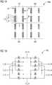
Das Bauelement
Die Pixel
Die den Pixeln
Anhand
Anhand
Die Pixel
Anhand der
Die Bauelemente
Die LED-Chips sind in der Erstreckungsrichtung
Einem bezüglich des ersten Pixels
Einem bezüglich des ersten Pixels
In anderen Worten werden einzelne LED-Chips zur sequentiellen Darstellung mehrerer Pixel verwendet. Eine mehrfache Zuordnung einzelner LED-Chips zu unterschiedlichen Pixeln erfolgt dabei auch bauelementübergreifend, d.h., einem Pixel können auch LED-Chips zugeordnet sein, die auf unterschiedlichen Bauelementen angeordnet sind. Insbesondere wird ausgenommen von denjenigen LED-Chips, die einer ersten oder letzten Reihe bzw. Spalte der Videowand
Die Bauelemente
Der anhand
Insgesamt sind für die Videowand
Um die Anzahl der Rückseitenkontakte der Bauelemente
In einem Daten- und Programmspeicher einer der Videowand
In einem Schritt
In einem darauffolgenden Schritt
Im Falle, dass ein LED-Chip als fehlerhaft erkannt wird, wird das Programm in einem Schritt
In dem Schritt
In dem Schritt
In einem anschließenden Schritt
In einem darauffolgenden Schritt
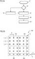
Anhand der
Die Bauelemente
Die LED-Chips sind in der Erstreckungsrichtung
Einem bezüglich des ersten, dritten und vierten Pixels
In anderen Worten werden einzelne LED-Chips zur sequentiellen Darstellung mehrerer Pixel verwendet. Eine mehrfache Zuordnung einzelner LED-Chips zu unterschiedlichen Pixeln erfolgt dabei auch bauelementübergreifend, d.h., einem Pixel können auch LED-Chips zugeordnet sein, die auf unterschiedlichen Bauelementen angeordnet sind. Insbesondere wird ausgenommen von denjenigen LED-Chips, die einer ersten oder letzten Reihe bzw. Spalte der Videowand
Die Bauelemente
Insgesamt sind für die Videowand
Um die Anzahl der Rückseitenkontakte der Bauelemente
Die Erfindung ist nicht durch die Beschreibung anhand der Ausführungsbeispiele auf diese beschränkt. Vielmehr umfasst die Erfindung jedes neue Merkmal sowie jede Kombination von Merkmalen, was insbesondere jede Kombination von Merkmalen in den Patentansprüchen beinhaltet, auch wenn dieses Merkmal oder diese Kombination selbst nicht explizit in den Patentansprüchen oder Ausführungsbeispielen angegeben ist.The description based on the exemplary embodiments is not restricted to the invention. Rather, the invention encompasses every new feature and every combination of features, which in particular includes every combination of features in the patent claims, even if this feature or this combination itself is not explicitly specified in the patent claims or exemplary embodiments.
BezugszeichenlisteList of reference symbols
- 1_R, 1_G, 1_R 1,2_B 1,2_G 1,2 R 3,4_B 3,4_G 3,4_R1_R, 1_G,
1_R 1,2_B 1,2_G 1,2R 3,4_B 3,4_G 3,4_R - LED-ChipLED chip
- 1,3_A 2,4_A1,
3_A 2,4_A - ElektrodenElectrodes
- PP
- PixelabstandPixel pitch
- DD.
- ChipabstandChip spacing
- dd
- VersatzOffset
- EE.
- ErstreckungsrichtungDirection of extension
- R, R1, R2, R3R, R1, R2, R3
- Reiheline
- SS.
- Spaltecolumn
- 10, 20, 30, 40 11, 21, 31, 41 12, 22, 32, 4210, 20, 30, 40 11, 21, 31, 41 12, 22, 32, 42
- Pixelpixel
- 100, 200, 300, 400 101, 201, 301, 401 102, 202, 302, 402100, 200, 300, 400 101, 201, 301, 401 102, 202, 302, 402
- BauelementComponent
- 1000, 1001, 10021000, 1001, 1002
- VideowandVideo wall
Claims (16)
Translated fromGermanPriority Applications (5)
| Application Number | Priority Date | Filing Date | Title |
|---|---|---|---|
| DE102019109137.3ADE102019109137A1 (en) | 2019-04-08 | 2019-04-08 | COMPONENT FOR A DISPLAY DEVICE, DISPLAY DEVICE AND METHOD OF OPERATING THE DISPLAY DEVICE |
| CN202080027383.5ACN113661535B (en) | 2019-04-08 | 2020-03-11 | Display device and method for operating the display device |
| JP2021558902AJP7288080B2 (en) | 2019-04-08 | 2020-03-11 | Components for display devices, display devices and methods of operating display devices |
| PCT/EP2020/056507WO2020207689A1 (en) | 2019-04-08 | 2020-03-11 | Component for a display device, display device, and method for operating the display device |
| US17/602,232US11749187B2 (en) | 2019-04-08 | 2020-03-11 | Component for a display device, display device and method of operating the display device |
Applications Claiming Priority (1)
| Application Number | Priority Date | Filing Date | Title |
|---|---|---|---|
| DE102019109137.3ADE102019109137A1 (en) | 2019-04-08 | 2019-04-08 | COMPONENT FOR A DISPLAY DEVICE, DISPLAY DEVICE AND METHOD OF OPERATING THE DISPLAY DEVICE |
Publications (1)
| Publication Number | Publication Date |
|---|---|
| DE102019109137A1true DE102019109137A1 (en) | 2020-10-08 |
Family
ID=69804894
Family Applications (1)
| Application Number | Title | Priority Date | Filing Date |
|---|---|---|---|
| DE102019109137.3APendingDE102019109137A1 (en) | 2019-04-08 | 2019-04-08 | COMPONENT FOR A DISPLAY DEVICE, DISPLAY DEVICE AND METHOD OF OPERATING THE DISPLAY DEVICE |
Country Status (5)
| Country | Link |
|---|---|
| US (1) | US11749187B2 (en) |
| JP (1) | JP7288080B2 (en) |
| CN (1) | CN113661535B (en) |
| DE (1) | DE102019109137A1 (en) |
| WO (1) | WO2020207689A1 (en) |
Families Citing this family (3)
| Publication number | Priority date | Publication date | Assignee | Title |
|---|---|---|---|---|
| US12185608B2 (en)* | 2021-01-28 | 2024-12-31 | Innolux Corporation | Light emitting device |
| TWI880062B (en)* | 2022-01-11 | 2025-04-11 | 隆達電子股份有限公司 | Inorganic light emitting diode display |
| US11955064B1 (en)* | 2022-10-12 | 2024-04-09 | Infineon Technologies Ag | Multi-pixel LED arrangements |
Family Cites Families (22)
| Publication number | Priority date | Publication date | Assignee | Title |
|---|---|---|---|---|
| US7091986B2 (en) | 1997-09-13 | 2006-08-15 | Gia Chuong Phan | Dynamic pixel resolution, brightness and contrast for displays using spatial elements |
| JP2000190564A (en)* | 1998-12-25 | 2000-07-11 | Canon Inc | Light source device and image forming apparatus |
| RU2249257C2 (en)* | 1999-03-24 | 2005-03-27 | Эвикс Инк. | Method and device for representing data of multicolor image of bite-wise displaying on pixel matrix display screen, on which lamps of three main colors are positioned |
| JP2000353825A (en) | 1999-06-09 | 2000-12-19 | Sony Corp | Manufacture of stage for mounting led nodule |
| US6224216B1 (en)* | 2000-02-18 | 2001-05-01 | Infocus Corporation | System and method employing LED light sources for a projection display |
| JP2002062825A (en) | 2000-08-18 | 2002-02-28 | Sony Corp | Image display device and method of manufacturing the same |
| TW540022B (en) | 2001-03-27 | 2003-07-01 | Koninkl Philips Electronics Nv | Display device and method of displaying an image |
| CN100395796C (en)* | 2005-07-08 | 2008-06-18 | 中国科学院长春光学精密机械与物理研究所 | A method of pixel multiplexing to improve display screen image resolution |
| JP2007286412A (en) | 2006-04-18 | 2007-11-01 | Seiwa Electric Mfg Co Ltd | Method for controlling lighting of led unit |
| JP2009186745A (en)* | 2008-02-06 | 2009-08-20 | Sharp Corp | LED display device |
| US8502758B2 (en) | 2009-12-10 | 2013-08-06 | Young Electric Sign Company | Apparatus and method for mapping virtual pixels to physical light elements of a display |
| CN102147064B (en)* | 2011-01-05 | 2014-03-26 | 深圳市众明半导体照明有限公司 | LED (Light Emitting Diode) module and lighting device |
| CN103325320B (en)* | 2013-07-06 | 2015-06-10 | 长春希达电子技术有限公司 | LED display screen with same-color chips arrayed diagonally and method for reusing pixels |
| CN204029292U (en)* | 2014-04-08 | 2014-12-17 | 深圳市奥蕾达科技有限公司 | A kind of wafer dispersion nation fixation element sequentially pulsed LED module |
| US9444015B2 (en)* | 2014-06-18 | 2016-09-13 | X-Celeprint Limited | Micro assembled LED displays and lighting elements |
| JP2017015943A (en) | 2015-07-01 | 2017-01-19 | 富士通株式会社 | Display control device, display control system, display control method and display control program |
| CN105913794A (en)* | 2016-01-26 | 2016-08-31 | 佛山市南海区联合广东新光源产业创新中心 | LED virtual display model |
| CN106448476A (en)* | 2016-07-28 | 2017-02-22 | 刘万斌 | Commercial induction cooker display screen interaction display method |
| CN106898601A (en) | 2017-02-15 | 2017-06-27 | 佛山市国星光电股份有限公司 | LED circuit board, triangle LED component and display screen that triangle is combined |
| JP6982287B2 (en) | 2017-03-13 | 2021-12-17 | 株式会社K工房 | Image display panel |
| KR20190114368A (en)* | 2018-03-30 | 2019-10-10 | (주)포인트엔지니어링 | Micro led semi-product module |
| CN109346004A (en) | 2018-12-19 | 2019-02-15 | 广州励丰文化科技股份有限公司 | A kind of control system of the diamond shape LED screen for display canopy of the heavens |
- 2019
- 2019-04-08DEDE102019109137.3Apatent/DE102019109137A1/enactivePending
- 2020
- 2020-03-11WOPCT/EP2020/056507patent/WO2020207689A1/ennot_activeCeased
- 2020-03-11CNCN202080027383.5Apatent/CN113661535B/enactiveActive
- 2020-03-11USUS17/602,232patent/US11749187B2/enactiveActive
- 2020-03-11JPJP2021558902Apatent/JP7288080B2/enactiveActive
Also Published As
| Publication number | Publication date |
|---|---|
| CN113661535A (en) | 2021-11-16 |
| WO2020207689A1 (en) | 2020-10-15 |
| JP7288080B2 (en) | 2023-06-06 |
| JP2022525816A (en) | 2022-05-19 |
| US20220180808A1 (en) | 2022-06-09 |
| US11749187B2 (en) | 2023-09-05 |
| CN113661535B (en) | 2024-09-03 |
Similar Documents
| Publication | Publication Date | Title |
|---|---|---|
| DE69800514T2 (en) | Printed circuit board with primary and secondary through holes | |
| DE10159444B9 (en) | Liquid crystal display screen and method of manufacturing the same | |
| DE102013114719B4 (en) | Organic light emitting display device | |
| DE102015223707A1 (en) | Array architecture with high pixel density | |
| WO2020207689A1 (en) | Component for a display device, display device, and method for operating the display device | |
| DE60016995T2 (en) | Plasma display panel | |
| DE102013106760A1 (en) | Display device with driver unit | |
| DE102016119267A1 (en) | Display device and its manufacturing method | |
| DE102015122340A1 (en) | ARRAY SUBSTRATE, LIQUID CRYSTAL DISPLAY FIELD AND ORGANIC LIGHT EMITTING DISPLAY FIELD | |
| DE102009012123A1 (en) | Light emitting diode and lighting device that uses them | |
| DE60128188T2 (en) | Plasma display device with alternately arranged sustaining electrodes | |
| DE112021008165T5 (en) | Wiring substrate, display substrate and display device | |
| DE202023103730U1 (en) | LED panel structures | |
| DE102016112104A1 (en) | MODULAR MODULE | |
| DE102018114175A1 (en) | Arrangement for a display and method | |
| DE112021005311T5 (en) | INDICATOR | |
| DE112020004819B4 (en) | Display device and display unit | |
| WO2013004547A1 (en) | High-voltage led multichip module and method for adjusting an led multichip module | |
| DE202006009689U1 (en) | Illuminating unit for full color LED display, has LEDs, e.g. red, green and blue LEDs, that are crosswisely arranged and have rectangular or trapezoidal or polygonal upper surface, where virtual pixel technique of display is applied to LEDs | |
| DE3434589C2 (en) | ||
| DE202023103729U1 (en) | LED array structures | |
| DE102012217534A1 (en) | Compensation of a color locus shift | |
| WO2017021451A1 (en) | Method for arranging a plurality of semiconductor structure elements on a substrate, and substrate comprising a plurality of semiconductor structure elements | |
| DE112021008474T5 (en) | Light-emitting substrate and display device | |
| DE102016112935B4 (en) | Array substrate, display panel, display device and method of manufacturing the same |
Legal Events
| Date | Code | Title | Description |
|---|---|---|---|
| R163 | Identified publications notified | ||
| R012 | Request for examination validly filed |