DE102017002616A1 - Process for the in-situ production of "Majorana materials - superconductor" hybrid networks, as well as a hybrid structure produced by the process - Google Patents
Process for the in-situ production of "Majorana materials - superconductor" hybrid networks, as well as a hybrid structure produced by the processDownload PDFInfo
- Publication number
- DE102017002616A1 DE102017002616A1DE102017002616.5ADE102017002616ADE102017002616A1DE 102017002616 A1DE102017002616 A1DE 102017002616A1DE 102017002616 ADE102017002616 ADE 102017002616ADE 102017002616 A1DE102017002616 A1DE 102017002616A1
- Authority
- DE
- Germany
- Prior art keywords
- layer
- majorana
- structured
- additional layer
- superconducting
- Prior art date
- Legal status (The legal status is an assumption and is not a legal conclusion. Google has not performed a legal analysis and makes no representation as to the accuracy of the status listed.)
- Pending
Links
Images


Classifications
- H—ELECTRICITY
- H10—SEMICONDUCTOR DEVICES; ELECTRIC SOLID-STATE DEVICES NOT OTHERWISE PROVIDED FOR
- H10N—ELECTRIC SOLID-STATE DEVICES NOT OTHERWISE PROVIDED FOR
- H10N60/00—Superconducting devices
- H10N60/01—Manufacture or treatment
- H10N60/0912—Manufacture or treatment of Josephson-effect devices
- B—PERFORMING OPERATIONS; TRANSPORTING
- B82—NANOTECHNOLOGY
- B82Y—SPECIFIC USES OR APPLICATIONS OF NANOSTRUCTURES; MEASUREMENT OR ANALYSIS OF NANOSTRUCTURES; MANUFACTURE OR TREATMENT OF NANOSTRUCTURES
- B82Y10/00—Nanotechnology for information processing, storage or transmission, e.g. quantum computing or single electron logic
- G—PHYSICS
- G06—COMPUTING OR CALCULATING; COUNTING
- G06N—COMPUTING ARRANGEMENTS BASED ON SPECIFIC COMPUTATIONAL MODELS
- G06N10/00—Quantum computing, i.e. information processing based on quantum-mechanical phenomena
- G06N10/40—Physical realisations or architectures of quantum processors or components for manipulating qubits, e.g. qubit coupling or qubit control
- H—ELECTRICITY
- H10—SEMICONDUCTOR DEVICES; ELECTRIC SOLID-STATE DEVICES NOT OTHERWISE PROVIDED FOR
- H10N—ELECTRIC SOLID-STATE DEVICES NOT OTHERWISE PROVIDED FOR
- H10N60/00—Superconducting devices
- H10N60/10—Junction-based devices
- H10N60/12—Josephson-effect devices
- H—ELECTRICITY
- H10—SEMICONDUCTOR DEVICES; ELECTRIC SOLID-STATE DEVICES NOT OTHERWISE PROVIDED FOR
- H10N—ELECTRIC SOLID-STATE DEVICES NOT OTHERWISE PROVIDED FOR
- H10N60/00—Superconducting devices
- H10N60/80—Constructional details
- H10N60/805—Constructional details for Josephson-effect devices
- H—ELECTRICITY
- H10—SEMICONDUCTOR DEVICES; ELECTRIC SOLID-STATE DEVICES NOT OTHERWISE PROVIDED FOR
- H10N—ELECTRIC SOLID-STATE DEVICES NOT OTHERWISE PROVIDED FOR
- H10N60/00—Superconducting devices
- H10N60/80—Constructional details
- H10N60/83—Element shape
Landscapes
- Engineering & Computer Science (AREA)
- Physics & Mathematics (AREA)
- Theoretical Computer Science (AREA)
- General Physics & Mathematics (AREA)
- Mathematical Physics (AREA)
- Data Mining & Analysis (AREA)
- Software Systems (AREA)
- Condensed Matter Physics & Semiconductors (AREA)
- Mathematical Analysis (AREA)
- Mathematical Optimization (AREA)
- Pure & Applied Mathematics (AREA)
- Computing Systems (AREA)
- General Engineering & Computer Science (AREA)
- Computational Mathematics (AREA)
- Evolutionary Computation (AREA)
- Artificial Intelligence (AREA)
- Manufacturing & Machinery (AREA)
- Chemical & Material Sciences (AREA)
- Nanotechnology (AREA)
- Crystallography & Structural Chemistry (AREA)
- Superconductor Devices And Manufacturing Methods Thereof (AREA)
- Crystals, And After-Treatments Of Crystals (AREA)
Abstract
Translated fromGermanDescription
Translated fromGermanDie Erfindung betrifft ein Verfahren zur Herstellung einer Vorrichtung, die es ermöglicht in einer inerten Atmosphäre und vorzugsweise bis hin zum Ultrahochvakuum, supraleitendesowie Majorana-Materialien in verschiedenen Geometrien und Dimensionen bis auf ein paar Nanometer genau zueinander ausgerichtet abzuscheiden und mit einer passivierenden Schutzschicht zu konservieren. Komplexe Netzwerke aus den genannten Materialien können mit der Vorrichtung fabriziert werden. Diese Netzwerke beinhalten als kleinste Subeinheit eine Hybridstruktur wie beispielsweise einen topologischen Josephson-Kontakt, können aber in einer weiteren Ausführung bis zu einer Vielzahl von topologischen Quantenbits darstellen. Das Verfahren garantiert die Konservierung der Oberflächeneigenschaften des Majorana-Materials sowie eine hohe Grenzflächenqualität zwischen dem Majorana-Material und dem Supraleiter.The invention relates to a method for producing a device which makes it possible to deposit in an inert atmosphere and preferably up to the ultra-high vacuum, superconducting and Majorana materials in different geometries and dimensions with a few nanometers aligned with each other and preserved with a passivating protective layer. Complex networks of said materials can be fabricated with the device. These networks, as the smallest subunit, contain a hybrid structure such as Josephson topological contact, but in yet another embodiment may represent up to a plurality of topological quantum bits. The process guarantees the preservation of the surface properties of the Majorana material as well as a high interfacial quality between the Majorana material and the superconductor.
Stand der TechnikState of the art
Zur Darstellung von Bits müssen unterscheidbare physikalische Zustände vorliegen, welche sich in der klassischen Transistortechnologie durch zwei unterscheidbare Spannungswerte definieren. Im Falle eines Quantencomputers werden diese Zustände von unterscheidbaren quantenmechanischen Zuständen dargestellt. Ein solcher Quantencomputer zeichnet sich aus durch eine große, im Extremfall beliebig große Anzahl von unterscheidbaren Zuständen, die die Bits, die sogenannten Quanten-Bits (Qubits), darstellen. Aus diesem Grund können gewisse Berechnungen auf einem Quantencomputer wesentlich schneller und effizienter gelöst werden. So hat Google im Januar 2016 gezeigt, dass sie mit ihrem D-wave Quantenannealer ein Problem ungefähr 100.000.000x schneller lösen konnten als mit einem klassischen Computer. Ein Quantenannealer ist eine spezielle Art von Quantencomputer, der sich jedoch lediglich für Optimierungsprobleme einsetzen lässt. Die gesamte Rechenleistung, die die Quantenmechanik ermöglicht, zeigt sich erst in einem sogenannten universellen Quantencomputer. Das Hauptproblem von universellen Quantencomputern ist, dass die sehr empfindlichen und kurzlebigen Quantenzustände nicht stabil sind und allein das Auslesen dieser Zustände zu einer Änderung des Zustandes führen kann. Die daraus resultierenden Fehler müssen nach jedem Rechenschritt umgehend korrigiert werden. Diese Fehlerkorrektur (engl. Error Correction) ist der Grund, warum die Entwicklung eines universellen Quantencomputers nur langsam vorangeht und innerhalb der letzten 30 Jahre noch kein universeller Quantencomputer mit einer zweistelligen Zahl an Qubits realisiert werden konnte. Auf dem Gebiet des fehlerkorrigierten Quantenrechnens hat Google Anfang 2016 ebenfalls einen Meilenstein gesetzt und den bisher leistungsstärksten fehlerkorrigierten universellen Quantencomputer gebaut. Anders als bei den 1000 Qubits des D-wave 2X Quantenannealers sind hier lediglich 8 Qubits implementiert. IBM hat ebenfalls einen ersten universellen Quantencomputer mit fünf Qubits entwickelt, der im Rahmen der Quantum Experience seit Mai 2016 sogar der Öffentlichkeit zugänglich gemacht wurde. Allerdings braucht man mindestens 50 Qubits um Berechnungen durchzuführen, die derzeit nicht einmal von modernen Supercomputern gelöst werden können [1].To represent bits, distinguishable physical states must be present, which in classical transistor technology are defined by two distinguishable voltage values. In the case of a quantum computer, these states are represented by distinguishable quantum mechanical states. Such a quantum computer is characterized by a large, in the extreme case arbitrarily large number of distinguishable states, which represent the bits, the so-called quantum bits (qubits). For this reason, certain calculations on a quantum computer can be solved much faster and more efficiently. For example, Google showed in January 2016 that they were able to solve a problem about 100,000,000 times faster with their D-wave quantum annealer than with a classic computer. A quantum annealer is a special type of quantum computer, but it can only be used for optimization problems. The entire computing power that quantum mechanics makes possible is only revealed in a so-called universal quantum computer. The main problem of universal quantum computers is that the very sensitive and short-lived quantum states are not stable and only the reading of these states can lead to a change of the state. The resulting errors must be corrected immediately after each calculation step. This error correction (error correction) is the reason why the development of a universal quantum computer is progressing slowly and within the last 30 years, no universal quantum computer could be realized with a two-digit number of qubits. In the field of error-corrected quantum computing, Google also set a milestone at the beginning of 2016, building the most powerful error-corrected universal quantum computer ever. Unlike the 1000 qubits of the D-wave 2X quantum annealer, only 8 qubits are implemented here. IBM has also developed a first universal quantum computer with five qubits, which has even been made available to the public as part of the Quantum Experience since May 2016. However, you need at least 50 qubits to perform calculations that can not even be solved by modern supercomputers [1].
Um das Ziel eines Quantencomputers mit 50 Qubits schnellstmöglich zu realisieren, konzentrieren sich wissenschaftliche und industrielle Institutionen auf eine relative junge Sparte des Quantencomputings, das so genannte topologische Quantencomputing. Die Tatsache, dass für diese Art von Quantencomputer in der Theorie keine und in der Praxis nur ein sehr geringes Maß an Fehlerkorrektur notwendig ist, macht diesen Ansatz besonders vielversprechend und rückt eine 50 Qubit Maschine in nahe Zukunft.To achieve the goal of a quantum computer with 50 qubits as fast as possible, scientific and industrial institutions are focusing on a relatively new branch of quantum computing, the so-called topological quantum computing. The fact that this type of quantum computer in theory requires little and in practice only a very small amount of error correction makes this approach particularly promising and puts a 50 qubit machine in the near future.
Wie bei konventionellen (nicht-topologischen) Quantencomputern müssen auch beim topologischen Quantencomputer Quantenobjekte bzw. -teilchen (Objekte, Teilchen oder Quasiteilchen, die den Gesetzen der Quantenmechanik folgen) aktiv in den Rechenprozess eingebunden werden und dazu auf einem Chip positioniert, separat angesteuert, manipuliert und ausgelesen werden. Das quantenmechanische Quasiteilchen, auf dessen Grundlage der topologische Quantencomputer rechnet, ist die sogenannte gebundene Majorana Nullmode (MZM, engl. Majorana Zero Mode). MZMs sind 0-dimensionale Quasiteilchenanregungen, die aufgrund ihrer nicht-ablischen Vertauschungsrelationen neue Konzepte für Fehlertoleranteres Quantencomputing versprechen.As in the case of conventional (non-topological) quantum computers, quantum objects or particles (objects, particles or quasiparticles that follow the laws of quantum mechanics) must also be actively integrated into the calculation process and positioned on a chip, separately controlled and manipulated and read out. The quantum mechanical quasiparticle, on the basis of which the topological quantum computer calculates, is the so-called bound Majorana Nullmode (MZM, English Majorana Zero Mode). MZMs are 0-dimensional quasiparticle excitations that promise new concepts for error-tolerant quantum computing due to their non-ablative commutation relationships.
MZMs entstehen, wenn man sogenannte Majorana-Materialien mit supraleitenden Materialien in Verbindung bringt. Als Majorana-Materialien bezeichnen wir in diesem Dokument alle Materialien, in denen Majorana Nullmoden entstehen, sobald man diese Materialien in Kontakt mit einem Supraleiter bringt und die zur Erzeugung der MZMs notwendigen Felder (E-Feld und B-Feld) anlegt. Majorana Materialien sind beispielsweise Diracmaterialien, welche sich wiederum in beispielhaft topologische Isolatoren und Weyl-Metalle unterteilen lassen, sowie „half-metals“, welche nicht zu verwechseln sind mit Halbmetallen (engl. semimetals), sowie III-V-Halbleiter Nanodrähte. Notwendigerweise besitzen Majorana-Materialien fermionische Zustände die keinen Spin-Freiheitsgrad besitzen (in der englischen Sprache und im weiteren Verlauf dieses Dokuments werden diese Zustände als „spinless fermions“ bezeichnet). In einer Teilmenge der Majorana-Materialien, den sogenannten topologischen Isolatoren (TIs), führt beispielsweise die Spin-Bahn-Wechseiwirkung im Festkörper dazu, dass für fermionische Zustände an der Oberfläche des TIs die Richtung des Spins direkt an den k-Vektor im Impulsraum gekoppelt ist. Induziert man in ein solches „spinless fermions“-System Supraleitung, entstehen unter geeigneten Umständen (räumliche Geometrie des Majorana-Materials, E- und B-Felder) MZMs.MZMs are created by associating so-called Majorana materials with superconducting materials. Majorana materials in this document are all materials in which majorana zero-modes are formed as soon as these materials are brought into contact with a superconductor and the fields required to produce the MZMs (E-field and B-field) are created. Majorana materials are, for example, Dirac materials, which in turn can be subdivided into exemplary topological insulators and Weyl metals, as well as "half-metals", which should not be confused with semi-metals (English semimetals), and III-V semiconductor nanowires. Necessarily, majorana materials have fermionic states that do not possess spin degree of freedom (in the English language, and later in this document, these states are referred to as "spinless fermions"). In a subset of the Majorana materials, the so-called topological insulators (TIs), for example, leads In the solid-state spin-orbit interaction, for fermion states at the surface of the TI, the direction of the spin is coupled directly to the k-vector in momentum space. If one induces superconductivity in such a "spinless fermions" system, MZMs are formed under appropriate circumstances (spatial geometry of the majorana material, E and B fields).
Signaturen von MZMs wurden zum ersten Mal 2012 von der Gruppe um Leo Kouwenhoven in InAs Nanodrähten nachgewiesen, und anschließend auch in anderen Materialsystemen nachgewiesen. Majorana Nullmoden entstehen grundsätzlich immer in Paaren und im Fall von 1D Strukturen tauchen die beiden Moden örtlich separiert an den beiden Enden der 1D Struktur in Form von 0D Anregungen auf. Zusammen formen die beiden Majoranas einen fermionischen Zustand. Dieser Zustand kann entweder von einem Elektron besetzt oder eben unbesetzt sein. Um herauszufinden, ob sich in den beiden Majoranas ein Elektron befindet oder nicht, muss man die beiden Majoranas aufeinander zubewegen. Sobald sie sich „berühren“ bzw. ihre Wellenfunktionen überlappen, fusionieren sie zu einem Elektron oder sie annilieren und es entsteht kein Elektron.Signatures of MZMs were detected for the first time in 2012 by the group around Leo Kouwenhoven in InAs nanowires, and subsequently detected in other material systems. In principle, majora zero modes are always formed in pairs, and in the case of 1D structures, the two modes appear locally separated at the two ends of the 1D structure in the form of 0D excitations. Together, the two majoranas form a fermionic state. This state can either be occupied by an electron or just be unoccupied. To find out whether there is an electron in the two majoranas or not, you have to move the two majoranas towards each other. As soon as they "touch" each other or their wave functions overlap, they fuse to an electron or they anneal and there is no electron.
Die beiden Zustände „kein Elektron“ und „ein Elektron“ bilden die beiden Eigenzustände des Majoranapaars, bzw. des Majorana Qubits, analog zu den Eigenzuständen „Spin-up“ und „Spin-down“ eines konventionellen Spinqubits.The two states "no electron" and "one electron" form the two eigenstates of the majoran aura, or of the majorana qubit, analogous to the eigenstates "spin-up" and "spin-down" of a conventional spin qubit.
Ein grundlegender Unterschied zu konventionellen Qubits liegt bei Majorana Qubits darin, dass beide Eigenzustände dieselbe Energie aufweisen, also entartet sind. Bei konventionellen Qubits gibt es immer einen angeregten Zustand und einen Grundzustand. Verweilt das Qubit zulange im angeregten Zustand, relaxiert es in den Grundzustand und die Information ist verloren. Das kann beim Majorana Qubit nicht passieren. Diese und weitere Eigenschaften führen dazu, dass Majorana Qubits theoretisch keine Fehlerkorrektur benötigen [2]. Diese Tatsache reduziert den technologischen Aufwand für eine 50 Qubit Maschine maßgeblich und macht das Konzept des topologischen Quantencomputings so attraktiv.A major difference to conventional qubits is in Majorana qubits in that both eigenstates have the same energy, that is degenerate. Conventional qubits always have an excited state and a ground state. If the qubit persists in the excited state for a long time, it relaxes into the ground state and the information is lost. That can not happen with the Majorana Qubit. These and other properties mean that Majorana Qubits theoretically do not need error correction [2]. This fact significantly reduces the technological complexity of a 50 qubit machine and makes the concept of topological quantum computing so attractive.
Um mit Majoranas Quantencomputing zu betreiben, also den Zustand eines bzw. mehrerer Qubits zu ändern, muss man diese 0-dimensionalen Objekte in einer 2-dimensionalen Ebene anordnen. Außerdem ist es wichtig, dass man sie umeinander herum und aufeinander zubewegen kann. Die Änderung des quantenmechanischen Zustandes eines 2-Majorana Systems erfolgt nämlich durch das umeinander herum Rotieren der beiden Majoranas. Wenn man ein System im Zustand |0> (=kein Elektron) initialisiert und anschließend die beiden Majoranas um 360° umeinander herum dreht, so ändert man den Zustand zu |1>. Wenn man die beiden Majoranas nun miteinander fusionieren lässt, misst man zu 100 % ein Elektron und zu 0 % einen unbesetzten Zustand. Für den Fall von einer 180° Drehung umeinander liegt die Wahrscheinlichkeit ein Elektron zu messen bei 50 %, bei 90° nur noch bei 25 % usw..In order to operate with Majorana's quantum computing, ie to change the state of one or more qubits, one must arrange these 0-dimensional objects in a 2-dimensional plane. It's also important to be able to move around and around each other. Namely, the change of the quantum mechanical state of a 2-majorana system occurs by rotating the two majoranas around each other. If one initializes a system in state | 0> (= no electron) and then rotates the two majoranas 360 ° around each other, one changes the state to | 1>. If you merge the two majoranas together, you measure 100% of an electron and 0% an unoccupied state. In the case of a 180 ° rotation around each other, the probability of measuring an electron is 50%, at 90 ° only 25%, and so on.
Im Prinzip besteht ein topologischer Quantencomputer also aus einer gewissen Anzahl an Majoranas, die in einer Ebene angeordnet sind und die gezielt umeinander herum gedreht (bzw. geflechtet = engl: to braid) werden können. Mit der Anzahl von Majoranas, steigen die Möglichkeiten der „Braid“-Operationen und damit die Leistungsfähigkeit des Quantencomputers. Die Herausforderung besteht darin, (Quasi)1D- Strukturen bzw. Nanodrähte so anzuordnen, dass man die Majorana Moden den Ansprüchen entsprechend bewegen kann.In principle, a topological quantum computer thus consists of a certain number of majoranas, which are arranged in one plane and which can be rotated around each other (or braid). With the number of majoranas, the possibilities of "braid" operations and thus the performance of the quantum computer increase. The challenge is to arrange (quasi) 1D structures or nanowires so that one can move the Majorana modes according to the requirements.
Es gibt verschiedene Ansätze Majorana Moden zu erzeugen und darauf aufbauend die ersten Netzwerke zu generieren. Die ersten Signaturen von Majorana Moden wurden 2012 in InAs Nanodrähten nachgewiesen [3]. Auf Grundlage von diesen und ähnlichen Konzepten wird intensiv geforscht, mit dem Ziel zeitnah erste Majorana Qubits zu bauen. So ist beispielsweise aus
Der Ansatz aus einzelnen Halbleiter-Nanodrähten Majorana-Qubits zu bauen hat zwei entscheidende Nachteile. Zum einen ist in diesen Nanodrähten ein relativ starkes Magnetfeld erforderlich, um in die topologische Phase zu gelangen. Lediglich in dieser Phase können Majorana Moden erzeugt werden [4]. Um weiterhin aus Halbleiter-Nanodrähten Qubits zu bauen, müssen die Nanodrähte manuell und Nanometer-genau zueinander ausgerichtet werden. Egal ob man mit einzelnen oder mit Netzwerken aus gewachsenen Nanodrähten arbeitet, erfordert die Skalierung dieses Ansatzes ein enormes Maß an Aufwand.The approach of building single semiconductor nanowires of majorana qubits has two major drawbacks. On the one hand, a relatively strong magnetic field is required in these nanowires in order to reach the topological phase. Only in this phase can Majorana modes be generated [4]. To continue to build qubits from semiconductor nanowires, the nanowires must be aligned manually and nanometer-to-each other. Regardless of whether you work with individual or with networks of grown nanowires, the scaling of this approach requires an enormous amount of effort.
Einige Majorana-Materialien, wie zum Beispiel topologische Isolatoren, weisen von Natur aus die erforderlichen topologischen Eigenschaften auf. Hier muss lediglich das chemische Potential innerhalb der intrinsischen Bulk Energielücke liegen, um Majorana Physik betreiben zu können. In 2016 wurden in zwei unabhängigen Experimenten erstmals Signaturen von Majorana Moden in topologischen Isolatoren gefunden. Sollten die räumlichen Dimensionen des topologischen Isolators derart eingeschränkt werden, dass sich eine Energielücke innerhalb der Dispersion der Oberflächenzustände ergibt, ist es ebenfalls notwendig ein/en Magnetfeld/magnetischen Fluss durch die Struktur anzulegen. Dieses Magnetfeld ist relativ gesehen zu den notwendigen Magnetfeldern zur Zeeman Aufteilung der Rashba Bänder in InAs Nanodrähten sehr klein. Die charakteristische Größe ist dabei ein halbes magnetisches Flussquant, was bei den im weiteren Text herangezogenen Dimensionen einem Magnetfeld von nicht mehr als 150 mT entspricht [5, 6].Some majorana materials, such as topological insulators, inherently have the required topological properties. Here only the chemical potential within the intrinsic bulk energy gap has to be in order to operate Majorana physics. In 2016, signatures of Majorana fads were found in topological insulators for the first time in two independent experiments. Should the spatial dimensions of the topological insulator be restricted such that there is an energy gap within the dispersion of surface states, it is also necessary to apply a magnetic field / magnetic flux through the structure. This magnetic field is very small relative to the necessary magnetic fields for Zeeman splitting the Rashba bands in InAs nanowires. The characteristic size is half a magnetic flux quantum, which corresponds to a magnetic field of not more than 150 mT for the dimensions used in the following text [5, 6].
Neben dem entscheidenden Vorteil, dass in diesen Materialien kein Magnetfeld zum Erzeugen der topologischen Phase benötigt wird, gibt es einen weiteren Vorteil:In addition to the decisive advantage that no magnetic field is required in these materials for generating the topological phase, there is another advantage:
Gewisse topologische Isolatoren, wie beispielsweise (Bi(1-X)Sbx)2Te3 mit 0 ≤ x ≤ 1, wachsen selektiv [z. B. auf Si (111) gegenüber SiO2 oder Si3N4] [7]. Vorstrukturen lassen sich ohne großen Aufwand sehr umfangreich und komplex vor dem Wachstum definieren per optischer oder Elektronenstrahllitografie definieren. Diese Technik ermöglicht es komplexe Geometrien in sehr kurzer Zeit zu realisieren.Certain topological insulators such as (Bi (1-X ) Sbx )2 Te3 where 0 ≤ x ≤ 1 grow selectively [e.g. On Si (111) over SiO2 or Si3 N4 ] [7]. Pre-structures can be easily and very complexly defined before growth defined by optical or electron beam lithography. This technique makes it possible to realize complex geometries in a very short time.
Die „spinless fermions“ in Majorana-Materialien befinden sich im Falle von topologischen Isolatoren an der Oberfläche des Festkörpers. Wird die Oberfläche des topologischen Isolators außerhalb einer inerten Umgebung der Umgebungsluft ausgesetzt, führt die daraufhin stattfindende Oxidation dazu, dass die Diraczustände, so nennt man das System der spinless fermions in der Oberfläche eines topologischen Isolators, und damit der Oberflächentransport gestört werden. Es hat sich herausgestellt, dass noch in der inerten Atmosphäre, insbesondere im Ultrahochvakuum, auf einem topologischen Isolator eine Passivierungsschicht zum Schutz des topologischen Isolators vor Oxidation beziehungsweise Degradierung der Oberflächenzustände angeordnet werden kann. Hierdurch können die Oberflächenzustände erhalten bleiben. Als Passivierungsschicht kann beispielsweise eine dünne Schicht Aluminium von ungefähr 2 nm Schichtdicke verwendet werden, welche vollständig durchoxidieren kann und so den topologischen Isolator schützt. Alternativ werden bereits auch Te-, Se- und weitere isolierende Schichten als Passivierungsschichten eingesetzt. Es ist also wichtig, vor dem Ausschleusen aus der inerten Atmosphäre und ggfs. dem Ultrahochvakuum (p ≤ 1 × 10⁻⁷ mbar, vorzugsweise p ≤ 1 × 10⁻⁸ mbar), die gesamte Oberfläche des topologischen Isolators zu versiegeln und somit die Oberflächenzustände für Majoranaphysik zu konservieren. Eine inerte Atmosphäre bezeichnet eine Atmosphäre, die angepasst an das (Majorana-) Material, jegliche (chemische) Reaktion der in der Atmosphäre befindlichen Atome und Moleküle mit der Oberfläche des Materials unterbindet.The spinless fermions in Majorana materials are located on the surface of the solid in the case of topological insulators. When the surface of the topological insulator is exposed to ambient air outside an inert environment, the resulting oxidation leads to disruption of the Dirac states, called the spinless fermion system in the surface of a topological insulator, and thus the surface transport. It has been found that, even in the inert atmosphere, in particular in the ultra-high vacuum, a passivation layer for protecting the topological insulator from oxidation or degradation of the surface states can be arranged on a topological insulator. As a result, the surface conditions can be maintained. As a passivation layer, for example, a thin layer of aluminum of about 2 nm layer thickness can be used, which can oxidize completely and thus protects the topological insulator. Alternatively, Te, Se and further insulating layers are also used as passivation layers. It is therefore important to seal the entire surface of the topological insulator, and thus the surface conditions, before discharging from the inert atmosphere and optionally the ultrahigh vacuum (p ≦ 1 × 10⁻⁷ mbar, preferably p ≦ 1 × 10⁻⁸ mbar) to preserve for marjoram physics. An inert atmosphere refers to an atmosphere that, adapted to the (majorana) material, prevents any (chemical) reaction of the atoms and molecules in the atmosphere with the surface of the material.
Damit Majorana Moden entstehen, muss neben der topologischen Phase als zweite Voraussetzung auch ein Supraleiter vorhanden sein. Zwei supraleitende Kontakte, die einen geringen Abstand (5 - 150 nm) aufweisen und die durch ein Material verbunden sind, welches von sich aus nicht supraleitend ist, aber durch die Anwesenheit der Supraleiter bei tiefen Temperaturen selber im Bereich zwischen den Kontakten supraleitend wird, nennt man Josephson Übergang. Handelt es sich bei dem „von sich aus nicht-supraleitenden“ Material um ein Majorana-Material, bezeichnet man den Josephson Übergang als topologischen Josephson Übergang. Der Josephson Übergang ist eines der simpelsten Hybridbauteile, bestehend aus Supraleiter und Majorana-Material, und der Grundbaustein für viele komplexere Bauteile. Es ist aus dem Stand der Technik bekannt, supraleitende Josephson-Kontakte ex situ aufzubringen. Hierzu kann das Majorana-Material, oder spezifischer der topologische Isolator, zunächst über ein vakuumbasiertes Beschichtungsverfahren bzw. Dünnschichttechnologie (physikalische Gasphasenabscheidung (PVD), chemische Gasphasenabscheidung (CVD), vorteilhaft Molekularstrahlepitaxie (MBE)) abgeschieden werden. Die supraleitenden Kontakte können dann im Anschluss durch Elektronenstrahllithographie (EBL) in einen dafür geeigneten Resist definiert und anschließend in einer anderen Anlage aufgedampft oder - gesputtert werden. Falls der topologische Isolator zuvor mit einem Capping versiegelt wurde, muss dies unmittelbar vor der Deposition des Supraleiters entfernt werden, da der Supraleiter in direktem Kontakt mit dem Majorana-Material stehen muss. Bei derartigem Vorgehen besteht regelmäßig die Gefahr, dass die Oberfläche des Majorana-Materiales vor der Aufbringung des supraleitenden Materiales bereits oxidiert bzw. mit der Umgebungsluft reagiert. Dies führt beispielsweise zu Defekten und zu amorphisierenden Oberflächenbereichen, d. h zu einer mit Störstellen und Unebenheiten behafteten Grenzfläche zwischen dem Majorana-Material und dem Supraleiter. Diese wirken sich nachteilig als Tunnelbarrieren aus. Solche Grenzflächen sind in der Regel nicht dazu geeignet Majorana-Physik zu betreiben.In order to create majorana fashions, a superconductor must be available as a second prerequisite, in addition to the topological phase. Two superconducting contacts which are closely spaced (5-150 nm) and which are connected by a material which is not intrinsically superconductive in nature but becomes superconducting by the presence of the superconductors at low temperatures itself in the region between the contacts man Josephson transition. If the "inherently non-superconducting" material is a majorana material, the Josephson transition is called the topological Josephson transition. The Josephson junction is one of the simplest hybrid components, consisting of superconductor and Majorana material, and the basic building block for many more complex components. It is known in the art to apply superconducting Josephson contacts ex situ. For this purpose, the Majorana material, or more specifically the topological insulator, first by a vacuum-based coating process or thin-film technology (physical vapor deposition (PVD), chemical vapor deposition (CVD), advantageously molecular beam epitaxy (MBE)) are deposited. The superconducting contacts can then be subsequently defined by electron beam lithography (EBL) in a suitable resist and then vapor-deposited or sputtered in another system. If the topological insulator has been previously capped, this must be removed immediately prior to deposition of the superconductor, since the superconductor must be in direct contact with the majorana material. In the case of such a procedure there is regularly the risk that the surface of the Majorana material already oxidises or reacts with the ambient air before the application of the superconducting material. This leads, for example, to defects and surface areas that become amorphous, i. h to an impurity and bumpy interface between the majorana material and the superconductor. These adversely affect as tunnel barriers. Such interfaces are usually not suitable to operate Majorana physics.
Für andere Materialsysteme, wie beispielsweise InAs, ist es ferner bekannt auf Dünnfilmen eine homogene Schicht aus supraleitendem Material, insbesondere Aluminium, in-situ aufzubringen [8]. Anschließend werden die supraleitenden Materialien chemisch und/oder physikalisch strukturiert. Dies erfolgt durch Entfernen von Teilbereichen der supraleitenden Schicht.For other material systems, such as InAs, it is also known on thin films to apply a homogeneous layer of superconducting material, in particular aluminum, in situ [8]. Subsequently, the superconducting materials are chemically and / or physically structured. This is done by removing portions of the superconducting layer.
Durch das Aufbringen der supraleitenden Materialien ohne die inerte Atmosphäre und insbesondere das Ultrahochvakuum zu verlassen, kann eine Grenzfläche von sehr hoher Qualität zwischen dem Majorana-Material (bzw. dem topologischen Isolator) und dem Supraleiter erzeugt werden. Nachteilig führt die Entfernung von Teilbereichen der supraleitenden Schicht auch immer zu einer Veränderung oder Zerstörung der Oberfläche des darunter befindlichen Materials. Dies führt insbesondere bei der Verwendung von topologischen Isolatoren zu einer chemischen Veränderung der Oberfläche.By applying the superconducting materials without leaving the inert atmosphere, and in particular the ultrahigh vacuum, a very high quality interface between the majorana material (or the topological insulator) can be obtained. and the superconductor. Disadvantageously, the removal of portions of the superconductive layer always leads to a change or destruction of the surface of the underlying material. This leads in particular to the use of topological insulators to a chemical change of the surface.
Ein Nanometer-genaues Entfernen einer auf einem Majorana-Material angeordneten supraleitenden Schicht und einer anschließenden, lokalen, Oxidation dieses Bereiches ist wegen der Oberflächeneigenschaften des Supraleiters in der Regel nicht möglich. Im Fall von Aluminium wäre die Oberfläche des Aluminiums dabei zudem regelmäßig zu rau.A nanometer-accurate removal of a arranged on a Majorana material superconducting layer and a subsequent, local, oxidation of this range is not possible because of the surface properties of the superconductor in the rule. In the case of aluminum, the surface of the aluminum would also be regularly too rough.
Aus dem Stand der Technik bekannt ist die so genannte Stencil Lithographie. Diese Technologie ermöglicht es, Teilbereiche eines Substrats oder Dünnfilms mittels einer Schattenmaske (Hart-Maske) mit einer zweiten strukturierten Schicht (in-situ) zu versehen [9, 10]. Der Einsatz von Hart-Masken ermöglicht die Strukturierung einer zweiten, zum Beispiel supraleitenden Schicht innerhalb der inerten Atmosphäre und vorteilhaft bis hin zum Ultrahochvakuum. Die Strukturierung erfolgt hier in Anlagen mit gerichtetem Materialfluss durch ein Abbilden der auf der Hart-Maske definierten Strukturen.Known from the prior art is the so-called stencil lithography. This technology makes it possible to provide partial regions of a substrate or thin film with a second structured layer (in situ) by means of a shadow mask (hard mask) [9, 10]. The use of hard masks allows the structuring of a second, for example, superconducting layer within the inert atmosphere and advantageously up to the ultra-high vacuum. The structuring takes place here in systems with directed material flow by mapping the structures defined on the hard mask.
Aufgabe der ErfindungObject of the invention
Aufgabe der Erfindung ist es, ein Verfahren bereit zu stellen, mit dem Majorana-Material - Supraleiter Strukturen, umfassend wenigstens ein strukturiertes Majorana-Material und wenigstens ein darauf angeordnetes supraleitendes Material, nachfolgend auch Hybridstrukturen genannt, als kleinste Einheit eines Majorana-Material-Supraleiter Hybridnetzwerkes, in wenigen Prozessschritten generiert werden können. Das Verfahren sollte einerseits eine hohe Qualität der Oberflächen und Grenzflächen sicherstellen und zudem eine Passivierung des strukturierten Majorana-Materials garantieren. Insbesondere sollte durch das Verfahren ermöglicht werden, dass die generierten Oberflächenzustände insbesondere für Majoranaphysik konserviert werden können.The object of the invention is to provide a method with the Majorana material - superconductor structures comprising at least one structured Majorana material and at least one superconducting material arranged thereon, also referred to below as hybrid structures, as the smallest unit of a Majorana material superconductor Hybrid network, can be generated in a few process steps. On the one hand, the process was intended to ensure a high quality of the surfaces and interfaces and, moreover, to guarantee a passivation of the structured Majorana material. In particular, it should be made possible by the method that the generated surface states can be preserved, in particular for majoranaphysics.
Ferner sollte das Verfahren es ermöglichen, dass das strukturierte Majorana-Material und das supraleitende Material mit einer hohen Genauigkeit relativ zueinander ausgerichtet werden können, und eine hohe Skalierbarkeit gewährleistet ist.Furthermore, the method should enable the structured Majorana material and the superconducting material to be aligned with high accuracy relative to each other, and high scalability is ensured.
Ferner ist es die Aufgabe der Erfindung, mit Hilfe des vorgenannten Verfahrens qualitativ hochwertige Hybridstrukturen bereit zu stellen, mit denen dann beliebig komplexe Netzwerke aus Majorana-Material - Supraleitern aufgebaut werden können.Furthermore, it is the object of the invention to provide high-quality hybrid structures with the aid of the aforementioned method, with which then arbitrarily complex networks of Majorana material superconductors can be constructed.
Lösung der AufgabeSolution of the task
Die Aufgaben der Erfindung werden gelöst durch ein Verfahren zur Herstellung einer Majorana-Material - Supraleiter Struktur, nachfolgend kurz Hybridstrukur genannt, umfassend wenigstens ein strukturiertes Majorana-Material, wenigstens ein darauf angeordnetes strukturiertes supraleitendes Material sowie eine Passivierungsschicht, die auf der freien Oberfläche des strukturierten Majorana-Materials angeordnet ist, gemäß Hauptanspruch.The objects of the invention are achieved by a method for producing a majorana material-superconductor structure, hereinafter referred to as hybrid structure, comprising at least one structured majorana material, at least one structured superconducting material arranged thereon and a passivation layer which is deposited on the free surface of the structured material Majorana material is arranged, according to the main claim.
Die Aufgaben werden ferner gelöst durch eine Hybridstruktur, umfassend wenigstens ein strukturiertes Majorana-Material, insbesondere umfassend wenigstens ein strukturiertes Majorana-Material in Form eines lateral gewachsenen (quasi) 1D Nanodrahts bzw. einer lateral gewachsenen (quasi) 1D Nanostruktur, und wenigstens ein darauf angeordnetes strukturiertes supraleitendes Material sowie eine Passivierungsschicht, die auf der freien Oberfläche des strukturierten Majorana-Materials angeordnet ist, gemäß Nebenanspruch sowie durch eine Verwendung einer solchen Hybridstruktur gemäß weiterem Nebenanspruch.The objects are further achieved by a hybrid structure comprising at least one structured majorana material, in particular comprising at least one structured majorana material in the form of a laterally grown (quasi) 1D nanowire or a laterally grown (quasi) 1D nanostructure, and at least one thereon arranged structured superconducting material and a passivation layer, which is arranged on the free surface of the structured Majorana material, according to independent claim and by use of such a hybrid structure according to another additional claim.
Vorteilhafte Ausgestaltungen des Verfahrens sowie der Vorrichtung und der Verwendung ergeben sich aus den jeweils hierauf rückbezogenen Patentansprüchen.Advantageous embodiments of the method and of the device and the use emerge from the respective claims appended hereto.
Beschreibung der ErfindungDescription of the invention
Die Erfindung betrifft ein Verfahren, bei dem mit Hilfe einer oberflächennahen Maske eine Majorana-Material - Supraleiter Struktur, kurz Hybridstruktur, hergestellt werden kann. Diese Hybridstruktur umfasst wenigstens ein strukturiertes Majorana-Material, welches im Rahmen dieser Erfindung definiert wird als ein lateral gewachsener (quasi) 1D Nanodraht oder eine lateral gewachsene (quasi) 1D Nanostruktur, wobei letztere beispielsweise in Form eines strukturierten topologischen Dünnfilms vorliegen kann. Neben dem strukturierten Majorana-Material weist die Hybridstruktur wenigstens ein auf diesem strukturierten Majorana-Material angeordnetes strukturiertes supraleitendes Material sowie eine Passivierungsschicht auf, die auf der freien Oberfläche des strukturierten Majorana-Materials, welches nicht durch das superleitende Material kontaktiert ist, angeordnet ist.The invention relates to a method in which with the aid of a near-surface mask a Majorana material - superconductor structure, short hybrid structure, can be produced. This hybrid structure comprises at least one structured majorana material, which in the context of this invention is defined as a laterally grown (quasi) 1D nanowire or a laterally grown (quasi) 1D nanostructure, the latter for example being in the form of a structured topological thin film. In addition to the structured Majorana material, the hybrid structure has at least one structured superconducting material arranged on this structured Majorana material and a passivation layer which is arranged on the free surface of the structured Majorana material which is not contacted by the superconducting material.
Bei den erfindungsgemäßen Strukturen wird durch in-situ und vorzugsweise durch epitaktisches Aufwachsen beider Schichten eine besondere Güte der Grenzfläche zwischen beispielhaft einem topologischen Isolator und einem supraleitenden Metall sichergestellt.In the structures according to the invention, a special quality of the interface between, for example, a topological insulator and a superconducting metal is ensured by in-situ and preferably by epitaxial growth of both layers.
Ferner kann mit dem erfindungsgemäßen Verfahren auch direkt bei der Herstellung eine schützende Passivierungsschicht über freiliegenden Bereichen des strukturierten Majorana-Materials erzeugt werden, die vorteilhaft dazu führt, dass dessen Oberflächenzustände weder zerstört noch verändert werden. Oberflächenzustände in topologischen Isolatoren werden auch als Diraczustände bezeichnet. Furthermore, with the method according to the invention, a protective passivation layer over exposed areas of the structured Majorana material can also be produced directly during the production, which advantageously leads to its surface states neither being destroyed nor altered. Surface states in topological insulators are also referred to as dirac states.
Bei dem erfindungsgemäßen Verfahren wird vorteilhaft neben einer aus dem Stand der Technik bekannten Maske zur strukturierten Aufbringung wenigstens eines supraleitenden Materials auf einem Majorana-Material (Schattenmaske, Hart-Maske, „Stencil Mask“) zuvor eine weitere Maske direkt auf dem Substrat erzeugt (Maske zur Erzeugung einer Vorstruktur, „Selective Area“), die dazu dient, das Majorana-Material in einer definierten Geometrie auf einem Substrat abzuscheiden. Die Ausbildung zweier Masken auf dem Substrat führt bei der Herstellung der Hybridstruktur im Anschluss vorteilhaft dazu, dass sowohl das abgeschiedene strukturierte Majorana-Material als auch die nachfolgend wenigstens eine supraleitende Struktur vorzugsweise schon während der Herstellung relativ zueinander exakt ausgerichtet werden können. Dadurch dass die Prozessschritte durchgehend in einer inerten Atmosphäre und vorzugsweise im Vakuum erfolgen, kann zudem erfindungsgemäß eine sehr gute Qualität und Güte der Grenzflächen der Hybridstruktur sichergestellt werden.In the method according to the invention, in addition to a mask known from the prior art for the structured application of at least one superconducting material on a majorana material (shadow mask, hard mask, stencil mask), a further mask is advantageously produced directly on the substrate (mask for generating a preliminary structure, "selective area"), which serves to deposit the Majorana material in a defined geometry on a substrate. The formation of two masks on the substrate in the production of the hybrid structure subsequently advantageously leads to the fact that both the deposited structured Majorana material and the subsequently at least one superconducting structure can be aligned exactly relative to one another during production. Because the process steps take place continuously in an inert atmosphere and preferably in a vacuum, it is also possible according to the invention to ensure a very good quality and quality of the interfaces of the hybrid structure.
Durch das erfindungsgemäße Verfahren können lateral gewachsene Heterostrukturen aus supraleitenden Materialien und Majorana-Materialien vorteilhaft von hoher Qualität und präziser Ausrichtung erzeugt werden. Verschiedene Geometrien und Dimensionen erlauben die strukturierte Definition von funktionellen Vorrichtungen, angefangen bei topologischen Josephson junctions bis hin zu komplexen Netzwerken für Anwendungen in skalierbaren topologischen Qubits als auch topologischen Quantenregistern.By means of the method according to the invention, laterally grown heterostructures of superconducting materials and Majorana materials can advantageously be produced of high quality and precise alignment. Different geometries and dimensions allow the structured definition of functional devices ranging from topological Josephson junctions to complex networks for applications in scalable topological qubits as well as topological quantum registers.
Sowohl das strukturierte Majorana-Material als auch das supraleitende Material werden erfindungsgemäß lateral gewachsen. Sowohl das strukturierte Majorana-Material als auch das supraleitende Material werden bei dem erfindungsgemäßen Verfahren strukturiert und relativ zueinander aufgebracht, ohne die Notwendigkeit diese Bearbeitung nach der Deponierung vorzunehmen. Gegenüber bisher bekannten Methoden der in-situ Strukturierung bietet das erfindungsgemäße Verfahren besondere Vorteile in der Abruptheit der Grenzflächen sowie der möglichen Dimensionierung der einzelnen funktionalen Schichten.Both the structured Majorana material and the superconducting material are grown laterally according to the invention. Both the structured Majorana material and the superconducting material are patterned in the method according to the invention and applied relative to each other, without the need to perform this treatment after landfilling. Compared to hitherto known methods of in-situ structuring, the method according to the invention offers particular advantages in terms of the abruptness of the interfaces and the possible dimensioning of the individual functional layers.
Solche erfindungsgemäß hergestellten und qualitativ hochwertigen Hybridstrukturen können vorzugsweise in topologischen Josephson-Kontakten aber auch in komplexen Bauteilen, wie topologischen SQUIDs (Abkürzung für superconducting quantum interference devices), topologischen Qubits (Abkürzung für Quantenbit) und topologischen Quantenregistern eingesetzt werden, welche sich als kleinste Einheit dem wohldefinierten Übergang eines topologischen Materiales und einem Supraleiter bedienen.Such high-quality hybrid structures produced according to the invention can be used preferably in topological Josephson junctions but also in complex components, such as topological SQUIDs (short for superconducting quantum interference devices), topological qubits (short for quantum bits) and topological quantum registers, which is the smallest unit serve the well-defined transition of a topological material and a superconductor.
Für die angesprochenen Anwendungen solcher Hybridstrukturen in der Majorana-Physik sowie dem darauf aufbauenden topologischen Quantum computing ist es notwendig, dass die herzustellenden Bauteile bzw. Grenzflächen eine hohe Qualität aufweisen, so wie sie die erfindungsgemäßen Strukturen liefern.For the mentioned applications of such hybrid structures in Majorana physics and the topological quantum computing based thereon, it is necessary for the components or interfaces to be produced to have a high quality, as they provide the structures according to the invention.
Unter einem Josephson-Kontakt, der beispielsweise solche erfindungsgemäßen Strukturen umfasst, versteht man zwei supraleitende Materialien, welche durch einen dünnen, nicht-supraleitenden Bereich, voneinander getrennt sind. Als Weaklink wird im Folgenden der Bereich verstanden, der im Josephson-Kontakt die beiden Supraleiter voneinander trennt und per Definition nicht-supraleitend ist.A Josephson junction comprising, for example, such structures according to the invention means two superconducting materials which are separated from one another by a thin, non-superconducting region. Weaklink is understood below to mean the region which, in Josephson contact, separates the two superconductors from one another and is by definition non-superconducting.
Die Erfindung wird nachfolgend am Beispiel eines topologischen Josephson-Kontaktes als einem Beispiel für eine erfindungsgemäße Hybridstruktur näher erläutert, ohne auf diese eingeschränkt zu sein. Der topologische Josephson-Kontakt umfasst dabei zwei supraleitende Materialien, welche lateral voneinander angeordnet sind, und ein strukturiertes Majorana-Material, welches den nicht-supraleitenden Bereich (Weaklink) auszeichnet.The invention is explained in more detail below using the example of a topological Josephson contact as an example of a hybrid structure according to the invention, without being restricted to these. The topological Josephson contact comprises two superconducting materials, which are arranged laterally from one another, and a structured Majorana material, which distinguishes the non-superconducting region (Weaklink).
Aus dem Stand der Technik ist bekannt, dass ein Weaklink als Zwischenbereich zwischen zwei Supraleitern, welcher ein topologisches Material umfasst, ebenfalls supraleitend sein kann, wenn die Distanz zwischen den Supraleitern ausreichend kurz ist. Ausreichend kurz ist eine solche Distanz, wenn sie kleiner ist als die Kohärenzlänge der gepaarten Elektronenzustände in dem topologischen Material. Die Kohärenzlänge liegt im Fall von Aluminium als supraleitendes Material bekanntermaßen bei 100 - 400 nm, je nach Qualität des kristallinen Materials als auch der Grenzschicht zwischen Supraleiter und topologischem Material. Bei der Verwendung von Niob ist dieser charakteristische Wert der Koheränzlänge aufgrund der größeren Sprungtemperatur etwas verringert und liegt in einem Bereich zwischen 50 - 250 nm.It is known from the prior art that a weave link as an intermediate region between two superconductors comprising a topological material may also be superconducting if the distance between the superconductors is sufficiently short. Such a distance is sufficiently short if it is smaller than the coherence length of the paired electron states in the topological material. The coherence length in the case of aluminum as a superconducting material is known to be 100-400 nm, depending on the quality of the crystalline material as well as the boundary layer between superconductor and topological material. When niobium is used, this characteristic value of the coherence length is somewhat reduced due to the higher transition temperature and is in a range between 50 and 250 nm.
Für den Fall eines Josephson-Kontaktes bedeutet Qualitätssicherung, dass einerseits ein guter Oberflächentransport im Bereich des Weaklinks sichergestellt wird, wozu eine in-situ Abdeckung (capping) notwendig ist, und dass der Kontakt andererseits eine saubere und scharfe Grenzfläche zwischen den Supraleitern und dem strukturierten Majorana-Material aufweist. Dies kann insbesondere durch in-situ und vorzugsweise durch ein epitaktisches Aufwachsen beider Schichten erreicht werden. Sowohl das strukturierte und relativ zueinander ausgerichtete Wachstum des strukturierten Majorana-Materials, das in-situ capping, als auch das in-situ Aufbringen der vorzugsweise epitaktischen, supraleitenden Kontakte wird durch das erfindungsgemäße Verfahren ermöglicht, ohne dabei eine inerte Atmosphäre und/oder ein Ultrahochvakuum zu verlassen.In the case of a Josephson junction, quality assurance means ensuring, on the one hand, good surface transport in the area of the wash link, requiring in-capping, and, on the other hand, providing a clean and sharp interface between the superconductors and the structured one Majorana Material has. This can be achieved in particular by in-situ and preferably epitaxial growth of both layers. Both the structured and relatively aligned growth of the structured Majorana material capping in situ, as well as the in-situ deposition of the preferably epitaxial superconducting contacts is made possible by the method of the invention, without an inert atmosphere and / or an ultra-high vacuum to leave.
Die Erfindung sieht dabei vor, zur Erzeugung einer solchen Hybridstruktur neben einer bereits bekannten stencil Maske (Schattenmaske) eine weitere Maske einzusetzen, über die die Geometrie des strukturierten Majorana-Materials definiert werden kann, und die ebenfalls fest mit dem Substrat verbunden ist.The invention provides for the generation of such a hybrid structure next to an already known stencil mask (shadow mask) to use a further mask over which the geometry of the structured Majorana material can be defined, and which is also firmly connected to the substrate.
Nachfolgend wird das erfindungsgemäße Verfahren zur Herstellung von Hybridstrukturen am Beispiel eines Josephson-Kontaktes unter Verwendung eines topologischen Isolators und supraleitender Metalle angegeben, ohne auf diese konkrete Ausgestaltung beschränkt zu sein.Hereinafter, the inventive method for the production of hybrid structures using the example of a Josephson contact using a topological insulator and superconducting metals is given, without being limited to this specific embodiment.
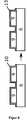
Die einzelnen Schritte des erfindungsgemäßen Verfahrens können anhand der
Die hier exemplarisch beschriebene Herstellung eines Josephson-Kontaktes ist nicht einschränkend zu verstehen, sondern dient zugleich als kleinste Einheit eines topologischen Qubits als Anschauung der im Anschluss aufgeführten Ausführungsbeispiele. Die Buchstaben der Prozessschritte zur Herstellung eines einzelnen topologischen Josephson-Kontaktes entsprechen dabei denen in den
Das erfindungsgemäße Verfahren ist in insgesamt drei Teilprozesse unterteilt.
- I. Die Vorbereitung des Substrates für ein strukturiertes Abscheiden des Majorana-Materials (Prozessschritt (I) „Selective Area“) durch Erzeugung einer ersten funktionellen Maske auf dem Substrat.
- II. Das Erzeugen einer oberflächennahen Schattenmaske (Stencil mask) zur definierten Aufbringung wenigstens eines supraleitenden Materials (Prozessschritt (II) „Stencil Mask“) ebenfalls auf dem Substrat.
- III. Das Verfahren während der Deposition innerhalb einer Vakuum-Kammer zum gerichteten und strukturierten Aufbringen der funktionellen Schichten (Prozessschritt (III) „Beschichtungsverfahren“).
- I. The preparation of the substrate for a structured deposition of the Majorana material (process step (I) "Selective Area") by creating a first functional mask on the substrate.
- II. The production of a near-surface shadow mask (stencil mask) for the defined application of at least one superconducting material (process step II stencil mask) likewise on the substrate.
- III. The process during deposition within a vacuum chamber for the directed and structured application of the functional layers (process step (III) "coating process").
Zur Unterscheidung verschiedener Möglichkeiten funktionelle Strukturen unter Zuhilfenahme der erzeugten Maske strukturiert zu deponieren, umfasst der dritte Teilprozess noch zwei verschiedene Variationen.In order to distinguish different possibilities of structurally depositing functional structures with the aid of the generated mask, the third subprocess comprises two different variations.
Teilprozess I: „Selective Area“
- I.A. Auf einem gereinigten Substrat (
1 ) wird flächig und unter Vakuum eine erste zusätzliche Schicht (2 ) aufgebracht. Das Substrat kann beispielhaft ein Siliziumwafer beliebiger Größe oder ein Siliziumwafer Teilstück sein. Unter einem gereinigten Substrat wird ein solches verstanden, welches mit einem, dem Fachmann bekannten, substrattypischen Standardverfahren zur Entfernung von Kontaminationen auf der Substratoberfläche behandelt wurde. Auf diese Weise wird eine Substratoberfläche bereitgestellt, welche nur substrateigene Verbindungen aufweist.Das Material des Substrates muss dafür geeignet sein, dass auf ihm ein topologischer Isolator aufwachsen kann. Für die erste Schicht (2 ) kann vorzugsweise ein Material eingesetzt werden, welches gegenüber dem Substrat und der zweiten Schicht (3) selektiv ätzbar ist.Dafür geeignet ist beispielsweise Siliziumdioxid (SiO2), wobei dieses vorzugsweise eine hohe Qualität aufweisen sollte und beispielhaft in einem Verfahren zur thermischen Umwandlung der Siliziumoberfläche erzeugt werden kann. Vorteilhaft weist dieses SiO2 eine sehr gute Ätz-Selektivität im Vergleich zum Silizium des Substrates (1 ) und der zweiten zusätzlichen Schicht (3 ) auf.Die SiO2-Schicht lässt sich zum Beispiel durch Flusssäure isotrop entfernen, wobei auf dem Substrat eine atomar plane Oberfläche erzeugt wird. Vorteilhaft weist die SiO2-Schicht ferner dielektrische Eigenschaften auf, wodurch Leckströme unterdrückt werden können. Aus dem Stand der Technik ist bekannt, dasseine 1bis 10 nm dünne SiO2-Schicht effektiv, bei der Verwendung von stöchiometrischem Silizium Nitrid (Si3N4) als zweite zusätzliche Schicht (3 ), Verspannungen mindert oder verhindert, welche das Si3N4 auf die Siliziumoberfläche ausüben kann. Verspannungen in dem Siliziumsubstrat können sich negativ auf die Bedeckung des Substrates durch die erste funktionelle Schicht (6 ) auswirken.Die gewählte Schichtdicke der ersten Schicht (2 ) sollte mögliche Verspannungen auf das Substrat kompensieren. Als Schichtdicke für die erste Schicht (2 ) wird einmöglicher Bereich von 1 bis 20 nm gewählt, vorzugsweiseein Bereich von 1und 5 nm. - I.B Auf der ersten zusätzlichen Schicht (
2 ) wird eine zweite zusätzliche Schicht (3 ) flächig und unter Vakuum aufgebracht. Diese Schicht (3 ) zeichnet sich dadurch aus, dass sie selektiv gegenüber der ersten zusätzlichen Schicht (2 ) entfernt werden kann. Die zweite Schicht sollte in dem angeführten Ausführungsbeispiel HF- beständig und insbesondere spannungsarm sein. In dem vorangegangenen Beispiel wird beispielhaft stöchiometrisches Siliziumnitrid (Si3N4) mit einer geringen Dichte von parasitären Wasserstoffverbindungen verwendet. Ein geeignetes Verfahren bietet hier das Abscheiden des Nitrids aus der Gasphase unter Niederdruck (eng. low pressure chemical vapour deposition, LP-CVD). Vorteilhaft lässt sich eine durchsichtige Si3N4-Schicht als Maske in nasschemischen Ätzverfahren verwenden. Die zweite zusätzliche Schicht (3 ) dient der Definition von Teilbereichen, auf denen der topologische Isolator selektiv gegenüber dem Siliziumsubstrat während des Wachstums nicht deponiert wird.Die Oberfläche der zweiten Schicht (3 ) schließt vorteilhaft mit der Oberfläche der ersten funktionalen Schicht (6 ) in Prozessschritt III.l ab. Die Schichtdicke sollte daherim Bereich von 5 bis 250 nm gewählt werden, vorzugsweiseim Bereich von 5 bis 100 nm. - I.C Nach dem Aufbringen der zweiten zusätzlichen Schicht (
3 ) erfolgt eine Strukturierung dieser Schicht, vorteilhaft über Elektronenstrahllithografie (electron beam lithography, EBL) unter Verwendung eines geeigneten Lackes oder Resist. Die in dem Resist definierten Strukturen werden nach der Entwicklung des Lackes mittels eines anschließenden Ätzverfahrens in die zweite zusätzliche Schicht (3 ) übertragen. Die zweite zusätzliche Schicht (3 ) wird insofern selektiv und strukturiert gegenüber der ersten zusätzlichen Schicht (2 ) teilweise entfernt.Vorteilhaft lassen sich durch das reaktive lonenätzen (engl. reactive ion etching, RIE) die gewünschten Strukturen in der zweiten zusätzlichen Schicht (3 ) präzise erzeugen, insbesondere in einer Si3N4-Schicht. Insbesondere werden anisotrope Strukturen durch dieses gerichtete Ätzverfahren erzeugt.In dem hier aufgeführten Beispiel eignet sich das reaktive lonenätzen unter Verwendung von beispielhaft Fluoroform und reinem Sauerstoff als reaktive Gasbestandteile. Alternativen wären beispielsweise die nasschemische Entfernung des Siliziumnitrids durch Phosphorsäure oder das physikalische Abtragen des Siliziumnitrids unter Zuhilfenahme von beschleunigten Ionen, z. B. in einer lonenstrahl Anlage (eng. Ion beam etching, IBE).In dem hier aufgeführten Verfahren zur Strukturierung der zweiten Schicht (3 ) werden beispielsweise dünne Gräben mit einer Breite von 10 - 10.000 nm, vorzugsweise von 30 - 200 nm, in der zweiten Schicht (3 ) definiert. Die Länge der erzeugten Gräben variiert dabei vorzugsweise zwischen 100 nm - 100 µm, vorzugsweise zwischen von 3 - 10 µm. Die Gräben können ebenfalls in Ring- oder Rechteckstrukturen definiert werden.Über die Verfahrensschritte A bis C wird somit eine erste funktionelle Maske ausbildet, mit deren Hilfe erfindungsgemäß und vorteilhaft eine definierte Geometrie des strukturierten Majorana-Materials ermöglicht wird. - I.D Die freigelegten Teilbereiche der ersten zusätzlichen Schicht (
2 ) werden selektiv gegenüber der zweiten zusätzlichen Schicht (3 ) sowie dem Substrat (1 ) entfernt. Vorzugsweise wird hier ein Prozess verwendet, welcher das Substrat (1 ) chemisch nicht umwandelt und/oder die Substratoberfläche beschädigt. Beispielhaft wird unter Verwendung der genannten Materialien verdünnte Flusssäure verwendet, welche das Siliziumdioxid selektiv ätzt und die Oberfläche des Siliziumsubstrates unverändert freilegt.Durch das isotrope Ätzverhalten des Siliziumdioxids in der verdünnten Flusssäure bildet sich ein Ätzprofil nahe dem gezeigten in, Prozessschritt D.
- IA on a purified substrate (
1 ) is surface and under vacuum, a first additional layer (2 ) applied. The substrate can be, for example, a silicon wafer of any size or a silicon wafer section. A purified substrate is understood to be one which has been treated with a standard substrate-typical process known to the person skilled in the art for the removal of contaminants on the substrate surface. In this way, a substrate surface is provided which has only intrinsic compounds. The material of the substrate must be suitable for allowing a topological insulator to grow on top of it. For the first layer (2 ), a material may be used which is selectively etchable with respect to the substrate and the second layer (3). Is suitable, for example, silicon dioxide (SiO2), this should preferably have a high quality and can be exemplified produced in a process for the thermal conversion of the silicon surface. This SiO2 advantageously has a very good etching selectivity in comparison to the silicon of the substrate (1 ) and the second additional layer (3 ) on. The SiO2 layer can be removed isotropically, for example by hydrofluoric acid, whereby an atomically planar surface is produced on the substrate. Advantageously, the SiO2 layer further has dielectric properties, whereby leakage currents can be suppressed. It is known from the prior art that a 1 to 10 nm thin SiO2 layer effectively, when using stoichiometric silicon nitride (Si3 N4 ) as a second additional layer (3 ), Reduces or prevents stresses that the Si3 N4 can exert on the silicon surface. Tensions in the silicon substrate can adversely affect the coverage of the Substrate through the first functional layer (6 ). The selected layer thickness of the first layer (2 ) should compensate for possible tension on the substrate. As layer thickness for the first layer (2 ), a possible range of 1 to 20 nm is selected, preferably a range of 1 and 5 nm. - IB on the first additional layer (
2 ), a second additional layer (3 ) applied flat and under vacuum. This layer (3 ) is characterized by being selective to the first additional layer (2 ) can be removed. The second layer should be HF-resistant and in particular low-stress in the cited embodiment. In the foregoing example, for example, stoichiometric silicon nitride (Si3 N4 ) having a low density of parasitic hydrogen compounds is used. A suitable method here is the deposition of the nitride from the gas phase under low pressure (narrow low pressure chemical vapor deposition, LP-CVD). Advantageously, a transparent Si3 N4 layer can be used as a mask in wet-chemical etching processes. The second additional layer (3 ) serves to define subregions on which the topological insulator is not selectively deposited relative to the silicon substrate during growth. The surface of the second layer (3 ) advantageously concludes with the surface of the first functional layer (6 ) in process step III.l. The layer thickness should therefore be selected in the range from 5 to 250 nm, preferably in the range from 5 to 100 nm. - IC After applying the second additional layer (
3 ), this layer is patterned, advantageously by electron beam lithography (EBL) using a suitable lacquer or resist. The structures defined in the resist are after the development of the paint by means of a subsequent etching process in the second additional layer (3 ) transfer. The second additional layer (3 ) is so far selective and structured compared to the first additional layer (2 ) partially removed. Advantageously, reactive ion etching (RIE) can be used to produce the desired structures in the second additional layer (FIG.3 ) produce precisely, especially in a Si3 N4 layer. In particular, anisotropic structures are produced by this directed etching process. In the example given here, reactive ion etching using exemplary fluoroform and pure oxygen as reactive gas constituents is suitable. Alternatives would be, for example, the wet-chemical removal of the silicon nitride by phosphoric acid or the physical removal of the silicon nitride with the aid of accelerated ions, for. In an ion beam etching (IBE). In the process for structuring the second layer (3 ), for example, thin trenches with a width of 10 - 10,000 nm, preferably from 30 - 200 nm, in the second layer (3 ) Are defined. The length of the trenches produced preferably varies between 100 nm and 100 μm, preferably between 3 and 10 μm. The trenches can also be defined in ring or rectangle structures. A first functional mask is thus formed via the method steps A to C, with the aid of which, according to the invention and advantageously, a defined geometry of the structured Majorana material is made possible. - ID The exposed parts of the first additional layer (
2 ) are selectively compared to the second additional layer (3 ) as well as the substrate (1 ) away. Preferably, here a process is used, which the substrate (1 ) does not chemically transform and / or damage the substrate surface. By way of example, dilute hydrofluoric acid is used using said materials, which selectively etches the silica and exposes the surface of the silicon substrate unaltered. As a result of the isotropic etching behavior of the silicon dioxide in the dilute hydrofluoric acid, an etching profile forms near that shown in FIG, Process step D.
Teilprozess II: „Stencil Mask“
- II.E Auf den in dem Teilprozess I erzeugten Strukturen wird in einem ersten Schritt flächig und unter Vakuum eine dritte zusätzliche Schicht (4) abgeschieden. Diese sollte selektiv gegenüber dem Substrat (
1 ) sowie der ersten (2 ) und zweiten (3 ) zusätzlichen Schicht zu entfernen sein. Beispielhaft wird hier Siliziumdioxid mit verringerter Qualität gegenüber der ersten Siliziumdioxid Schicht (2 ) verwendet, sowie es aus der Gasphase bei Niederdruck (low pressure chemical vapour deposition, LP-CVD) abgeschieden werden kann. Diese zweite Schicht Siliziumdioxid (4 ) wird deutlich schneller in verdünnter Flusssäure ätzen, sodass durch die Wahl der Ätzzeit diese Schicht selektiv gegenüber der ersten Siliziumdioxid Schicht (2 ) entfernt werden kann.Die gewählte Schichtdicke der dritten zusätzlichen Schicht (4 ) definiert den Abstand der oberflächennahen Maske (Schattenmaske) von der Substratoberfläche (1 ). Auf der Substratoberfläche werden im Teilprozess III bis zu vier funktionelle Schichten abgeschieden. Als Schichtdicke für die dritte zusätzliche Schicht (4 ) wird daherein Bereich von 5 bis 500 nm gewählt, vorzugsweiseein Bereich von 10 und 150 nm. - II.F Auf der dritten zusätzlichen Schicht (
4 ) wird eine vierte zusätzliche Schicht (5) flächig und unter Vakuum aufgebracht. Diese sollte selektiv gegenüber der dritten zusätzlichen Schicht (4 ) zu entfernen sein. Bei erneuter Verwendung von Siliziumnitrid können die in Prozessschritt I.C erwähnten Verfahren herangezogen werden. - II.G Die vierte zusätzliche Schicht (
5 ) wird selektiv gegenüber der dritten zusätzlichen Schicht (4 ) teilweise entfernt. Die zu erzeugenden Strukturen variieren, je nach gewünschter Vorrichtung. Verschiedene Ausführungen der Strukturen sind beispielhaft in dem Abschnitt mit den Ausführungsbeispielen erläutert. Die Strukturen beinhalten dabei sowohl große Flächen als auch kleine, schmale Übergänge, welche beide relativ zu den erzeugten Strukturen in der ersten zusätzlichen Schicht (2 ) ausgerichtet sind. Die genannten Übergänge, welche final Josephson-Kontakte definieren, haben mindestens die Breite der zuvor in Prozessschritt I.C erzeugten Strukturen in der ersten zusätzlichen Schicht (2 ) und einen lateralen Abstand zueinander von 10 - 500 nm, vorzugsweise 10 - 200 nm. Dieser schmale Bereich wird im Nachfolgenden als Nanobrücke bezeichnet. - II.H Die dritte zusätzliche Schicht (
4 ) wird selektiv gegenüber dem Substrat (1 ) als auch der ersten (2 ), zweiten (3 ) sowie der vierten zusätzlichen Schicht (5 ) entfernt. Dabei werden die in Schritt II.G freigelegten Bereiche entfernt. Notwendig für das erfindungsgemäße Verfahren ist, dass die dritte zusätzliche Schicht (4 ) isotrop in allen Richtungen entfernt wird. Daraus resultiert, dass jegliches Material der dritten zusätzlichen Schicht (4 ) unterhalb der in Schritt II.G definierten Nanobrücken entfernt wird. Zusätzlich werden die in dem Teilverfahren I definierten Strukturen teilweise freigelegt. Die Nanobrücken befinden sich ab diesem Zeitpunkt teilweise frei schwebend über dem Substrat (1 ).Über die Verfahrensschritte D bis F wird insofern eine zweite funktionelle Maske ausbildet, die häufig auch als Schattenmaske bezeichnet wird.
- II.E On the structures produced in the sub-process I, in a first step, a third additional layer (4) is deposited flat and under vacuum. This should be selective to the substrate (
1 ) as well as the first (2 ) and second (3 ) to remove additional layer. By way of example, reduced-quality silicon dioxide is here compared to the first silicon dioxide layer (2 ) as it can be deposited from the gas phase at low pressure (low pressure chemical vapor deposition, LP-CVD). This second layer of silica (4 ) will etch much faster in dilute hydrofluoric acid, so that by the choice of the etching time, this layer is selectively opposite to the first silicon dioxide layer (2 ) can be removed. The selected layer thickness of the third additional layer (4 ) defines the distance of the near-surface mask (shadow mask) from the substrate surface (1 ). On the substrate surface in the sub-process III up to four deposited functional layers. As layer thickness for the third additional layer (4 ), therefore, a range of 5 to 500 nm is selected, preferably a range of 10 and 150 nm. - II.F On the third additional layer (
4 ) a fourth additional layer (5) is applied flat and under vacuum. This should be selective to the third additional layer (4 ) be removed. If silicon nitride is used again, the methods mentioned in process step IC can be used. - II.G The fourth additional layer (
5 ) is selectively compared to the third additional layer (4 ) partially removed. The structures to be produced vary, depending on the desired device. Various embodiments of the structures are exemplified in the section with the embodiments. The structures include both large areas and small, narrow transitions, both of which are relative to the structures generated in the first additional layer (FIG.2 ) are aligned. The named transitions, which define final Josephson junctions, have at least the width of the structures previously generated in process step IC in the first additional layer (FIG.2 ) and a lateral distance from each other of 10 - 500 nm, preferably 10 - 200 nm. This narrow region is hereinafter referred to as nanobrücke. - II.H The third additional layer (
4 ) is selectively opposite to the substrate (1 ) as well as the first (2 ), second (3 ) and the fourth additional layer (5 ) away. The areas exposed in step II.G are removed. It is necessary for the method according to the invention that the third additional layer (4 ) is removed isotropically in all directions. As a result, any material of the third additional layer (4 ) is removed below the nano bridges defined in step II.G. In addition, the structures defined in subprocess I are partially exposed. From this point on, the nanoblocks are partly floating above the substrate (1 ). By way of method steps D to F, a second functional mask is thus formed, which is often referred to as a shadow mask.
Die beiden Teilprozesse I und II dienen insoweit der Vorbereitung zur eigentlichen Abscheidung bzw. Generierung der funktionalen Schichten der Hybridstrukturen auf dem Substrat.The two sub-processes I and II serve to prepare for the actual deposition or generation of the functional layers of the hybrid structures on the substrate.
Die nachfolgenden Verfahrensschritte I bis K werden nacheinander in einer inerten Atmosphäre durchgeführt, ohne das Vakuum, und hier insbesondere das Ultrahochvakuum (p ≤ 1 × 10⁻⁷ mbar, vorzugsweise p ≤ 1 × 10⁻⁸ mbar), zu unterbrechen. Als eine inerte Atmosphäre wird beispielsweise reines N2-Gas angesehen.The following process steps I to K are carried out successively in an inert atmosphere, without interrupting the vacuum, and in particular the ultra-high vacuum (p ≦ 1 × 10⁻⁷ mbar, preferably p ≦ 1 × 10⁻⁸ mbar). As an inert atmosphere, for example, pure N2 gas is considered.
Teilprozess III: „Beschichtungsverfahren“ Variante A
- III.l Die Probe mit den Nanobrücken sowie den teilweise freigelegten Flächen des Substrates (
1 ) wird für die Abscheidung der funktionalen Schichten/Strukturen in eine Vakuumkammer, z. B in die einer Molekularstrahl Epitaxie Anlage, überführt. Dieser Verfahrensschritt kann aber auch in anderen Beschichtungsanlagen stattfinden, in der das Wachstum teilweise gerichtet ausgeführt wird. Beispielhaft ist hier das Wachstum von III/V er Nanodrähten in einer chemischen Gasphasenabscheidungsanlage (eng. chemical vapor deposition CVD) zu nennen. Es wird die erste funktionale Schicht (6 ) abgeschieden. Diese Schicht muss selektiv auf der freigelegten Substratoberfläche (1 ) wachsen, während sich auf den freiliegenden Oberflächen der zusätzlichen Schichten (2 ,3 ) notwendig und auf den Oberflächen der zusätzlichen Schichten (4 ,5 ) vorteilhaft, kein Material abscheidet. Die erste funktionale Schicht (6 ) umfasst Majorana-Materialien.Beispielhaft wachsen topologische Isolatoren der Form (BixSb1-x)2(TeySe1-y)3, mit 0 ≤ x ≤ 1 und 0 ≤ y ≤ 1, auf einer Silizium (111) Oberfläche selektiv gegenüber Siliziumdioxid (2 ,4 ) und Siliziumnitrid (3 ,5 ) Oberflächen.Diese Abscheidung erfolgt über eine Substratrotation von 1 - 500 min-1, wodurch garantiert wird, dass der topologische Isolator ebenfalls auf den freigelegten Teilbereichen unterhalb der Nanobrücken aufwächst.Die durch die Verfahrensschritte A bis C erzeugte erste funktionale Maske definiert dabei die Struktur des Majorana-Materials.Die Schichtdicke wird dabei insbesondere so eingestellt, dass die Oberfläche des topologischen Dünnfilms (6 ) vorzugsweise mit der freigelegten Oberfläche der zweiten Schicht (3 ) abschließt. - III.J Ebenfalls unter Substratrotation wird eine zweite funktionale Schicht (7), welche eine native Oxidationsschicht auszubilden vermag, beispielhaft Aluminium oder Niob oder Wolfram, flächendeckend aufgebracht. Vorzugsweise wird ein supraleitendes Metall verwendet, beispielhaft Aluminium oder Niob. Diese Schicht wird aufgrund der Substratrotation ebenfalls unterhalb der Nanobrücken deponiert.In der hier beschriebenen Ausführung darf die Schichtdicke der zweiten funktionalen Schicht (
7 ) nicht die Dicke des nativen Oxides des jeweilig gewählten Materials überschreiten, um in nachfolgenden Schritten eine Passivierungsschicht für den topologischen Isolator ausbilden zu können.In einer Ausgestaltung des Verfahrens wird ein Dünnfilm, umfassend Aluminium, aufgebracht, da in Aluminium vorteilhaft gezielt eine Passivierungsschicht ausgebildet werden kann. Beispielsweise kann der Dünnfilm, umfassend Aluminium, mit einer Schichtdicke von maximal 3 nm aufgebracht werden, weil bei dieser Schichtdicke sichergestellt ist, dass bei einer nachfolgenden Oxidation die Aluminiumschicht als zweite funktionale Schicht (7 ) vollständig durchoxidiert. - III.K Eine dritte funktionale Schicht (
8 ), umfassend ein supraleitendes Material, beispielhaft Aluminium oder Niob, wird ohne Substratrotation auf Teilbereichen der zweiten funktionalen Schicht (7 ) strukturiert aufgebracht. Die in der vierten zusätzlichen Schicht (5 ) definierten Nanobrücken schatten den Atom-/Molpkularfluss teilweise ab. Durch diese teilweise Abschattung des Atom-/Molekularflusses wird die zweite funktionale Schicht (7 ) nicht komplett flächig, sondern nur in Teilbereichen beschichtet.Die Schichtdicke des nun deponierten Materials (8 ) sollte einerseits mindestens die kritische Dicke für den Erhalt der supraleitenden Eigenschaften des Materials betragen, andererseits aber die Dicke eines in einem nachfolgenden Schritt gebildeten nativen Oxides des verwendeten Materials nicht unterschreiten.Zusätzlich sollte die Schichtdicke der dritten funktionalen Schicht (8 ) nicht den Abstand zwischen Oberfläche der zweiten funktionalen Schicht (7 ) und der Unterkante der vierten zusätzlichen Schicht (5 ) überschreiten, da sonst eine unerwünschte Kontaktierung der generierten Hybridstruktur und der Schattenmaske nicht ausgeschlossen werden kann.Die Schichtdicke der deponierten Teilbereiche (8 ) beträgt insofern regelmäßig 5 - 500 nm, je nach gewählter Schichtdicke der ersten zusätzlichen Schicht (2 ). Vorzugsweise sollte die Schichtdicke zwischen 30 und 100 nm zur Sicherstellung der supraleitenden Eigenschaften der meisten supraleitenden Metalle gewählt werden, wobei auch die nachfolgende Ausbildung der Oxidschicht mit berücksichtigt werden sollte.Das Material der zweiten funktionalen Schicht (7 ) kann identisch zu dem Material der dritten funktionalen Schicht (8 ), also ein supraleitendes Material, gewählt werden. Die beiden Materialien können aber auch verschieden gewählt werden, da für die Funktion der zweiten funktionalen Schicht eine Supraleitung nicht zwingend erforderlich ist, sondem die Ausbildung einer nativen Oxidschicht als Passivierungsschicht vorrangig ist.So ist es bei dem erfindungsgemäßen Verfahren beispielsweise von Vorteil, Titan als zweite funktionale Schicht (7 ) zu wählen, da es als Interdiffusionsbarriere zwischen der ersten funktionalen Schicht (6 ) und der dritten funktionalen Schicht (8 ) dienen kann, jedoch ein anderes supraleitendes Metall, beispielsweise Aluminium oder Niob, als dritte funktionale Schicht (8 ) zu wählen, da diese Metalle besonders vorteilhafte supraleitende Eigenschaften gegenüber dem Titan aufweisen.
- III.l The sample with the nano-bridges as well as the partially exposed surfaces of the substrate (
1 ) is used for the deposition of the functional layers / structures in a vacuum chamber, for. B into which a molecular beam epitaxy plant, transferred. However, this process step can also take place in other coating plants in which the growth is carried out partially directed. Exemplary here is the growth of III / V he nanowires in a chemical vapor deposition (chemical vapor deposition CVD) to call. It becomes the first functional layer (6 ) deposited. This layer must be selectively deposited on the exposed substrate surface (1 ), while on the exposed surfaces of the additional layers (2 .3 ) and on the surfaces of the additional layers (4 .5 ) advantageous, no material separates. The first functional layer (6 ) includes Majorana materials. By way of example, topological insulators of the form (Bix Sb1-x )2 (Tey Se1-y )3 , with 0 ≦ x ≦ 1 and 0 ≦ y ≦ 1, grow selectively on a silicon (111) surface compared with silicon dioxide (2 .4 ) and silicon nitride (3 .5 ) Surfaces. This deposition takes place via a substrate rotation of 1 - 500 min-1 , which guarantees that the topological insulator also grows on the uncovered subregions below the nanobars. The first functional mask generated by method steps A to C defines the structure of the majorana material. The layer thickness is in particular adjusted so that the surface of the topological thin film (6 ) preferably with the exposed surface of the second layer (3 ) completes. - III.J Also under substrate rotation, a second functional layer (7), which is able to form a native oxidation layer, for example aluminum or niobium or tungsten, is applied over the entire surface. Preferably, a superconducting metal is used, exemplified by aluminum or niobium. This layer is also deposited below the nano bridges due to substrate rotation. In the embodiment described here, the layer thickness of the second functional layer (
7 ) do not exceed the thickness of the native oxide of the particular material chosen, in subsequent steps a Passivation layer for the topological insulator to be able to train. In one embodiment of the method, a thin film, comprising aluminum, is applied, since a passivation layer can advantageously be specifically formed in aluminum. For example, the thin film, comprising aluminum, can be applied with a layer thickness of at most 3 nm, because at this layer thickness it is ensured that in a subsequent oxidation the aluminum layer is used as a second functional layer (7 ) completely oxidized. - III.K A third functional layer (
8th ), comprising a superconducting material, for example aluminum or niobium, is applied to subregions of the second functional layer (without substrate rotation).7 ) structured applied. The in the fourth additional layer (5 ) defined nano-bridges partially shadow the atomic / molecular flow. Due to this partial shadowing of the atomic / molecular flow, the second functional layer (7 ) not completely flat, but only partially coated. The layer thickness of the now deposited material (8th ) should on the one hand be at least the critical thickness for obtaining the superconducting properties of the material, but on the other hand should not be less than the thickness of a native oxide formed in a subsequent step of the material used. In addition, the layer thickness of the third functional layer (8th ) not the distance between the surface of the second functional layer (7 ) and the lower edge of the fourth additional layer (5 ), since otherwise unwanted contacting of the generated hybrid structure and the shadow mask can not be excluded. The layer thickness of the deposited subregions (8th ) is in this respect regularly 5 - 500 nm, depending on the selected layer thickness of the first additional layer (2 ). Preferably, the layer thickness should be between 30 and 100 nm to ensure the superconducting properties of most superconducting metals, whereby the subsequent formation of the oxide layer should also be taken into account. The material of the second functional layer (7 ) can be identical to the material of the third functional layer (8th ), that is, a superconducting material. However, the two materials can also be chosen differently, since superconductivity is not absolutely necessary for the function of the second functional layer, but the formation of a native oxide layer as the passivation layer is a priority. For example, it is advantageous in the process according to the invention to use titanium as the second functional layer (7 ), as it acts as an interdiffusion barrier between the first functional layer (6 ) and the third functional layer (8th ), but another superconducting metal, for example aluminum or niobium, as the third functional layer (8th ), since these metals have particularly advantageous superconducting properties compared to titanium.
Teilverfahren III: „Beschichtungsverfahren“ Variante B
- III.l Dieser Verfahrensschritt entspricht dem der Variante A.
- III.J' Eine zweite funktionale Schicht (
9 ), umfassend supraleitendes Material, beispielhaft Aluminium oder Niob, wird ohne Substratrotation auf Teilbereichen der ersten funktionalen Schicht (strukturiertes Majorana-Material) (6 ) aufgebracht. Die in der vierten zusätzlichen Schicht (5 ) definierten Nanobrücken schatten dabei den Atom-/Molekularfluss teilweise ab. Ähnlich wie bei III.K wird durch diese teilweise Abschattung des Atom-/Molekularflusses das strukturierte Majorana-Material (6 ) nicht komplett flächig, sondern strukturiert nur in Teilbereichen mit dem supraleitenden Material der zweiten funktionalen Schicht (9 ) beschichtet.In einer alternativen Ausführung kann die zweite funktionale Schicht (9 ) auch als ein Schichtsystem, bestehend aus einer dünnen Interdiffusionsbarriere und einer dicken supraleitenden Schicht, aufgebracht werden. Als Material für die Interdiffusionsbarriere kann vorzugsweise ein Metall oder ein Supraleiter gewählt werden. Bei der Schichtdicke der supraleitenden Schicht ist erneut die kritische Dicke zum Erhalt der Supraleitung zu beachten. Als Interdiffusionsbarriere sind aus der Literatur beispielhaft dünne Schichten aus Platin, Wolfram oder Titan bekannt. Bei der Wahl eines nicht-supraleitenden Materiales als Interdiffusionsbarriere ist zu beachten, dass diese dünn genug gewählt ist, sodass die proximity induzierte Supraleitung über den definierten Weaklink gewährleistet ist.Die Dicke des deponierten Materials sollte mindestens die kritische Dicke für den Erhalt der supraleitenden Eigenschaften des Materials betragen, wobei zusätzlich die Schichtdicke des nativen Oxides berücksichtigt werden muss. Diese bildet sich aus, wenn das verwendete Material nach der Abscheidung mit Luftsauerstoff oder Sauerstoff in beliebiger anderer Form in Berührung kommt. Vorteilhaft beträgt die Dicke der Teilbereiche der zweiten funktionalen Schicht (9 ) daher zwischen 50 - 100 nm, wobei die Dicke des Materials nicht den Abstand zwischen Oberfläche der ersten funktionalen Schicht (6 ) und der vierten zusätzlichen Schicht (5 ) überschreiten sollte. - III.K' Eine dritte funktionale Schicht (
10 ), umfassend ein elektrisch isolierendes Material, wird auf die zweite funktionale Schicht (9 ) / das Schichtsystem, sowie die freiliegenden Bereiche der ersten funktionalen Schicht (6 ), flächendeckend aufgebracht. Diese Definition schließt oxidierende Metalle, wie in Prozessschritt III.J genannt, ein.Vorteilhaft können in dieser Ausgestaltung des Teilverfahrens III aber auch andere Materialien zum Schutz der Oberfläche und der Oberflächenzustände des strukturierten Majorana-Materials in den in Prozessschritt III.J' erzeugten Teilbereichen verwendet werden. Die verwendeten Materialien sollten dabei eine ausreichend große Bandlücke aufweisen, so dass in dem technisch relevanten Temperaturbereich, unter Berücksichtigung der tatsächlichen Elektronentemperatur, kein koheräntes Tunneln von Ladungsträgern in dem gewählten Material auftreten kann. Der technisch relevante Bereich ist definiert durch die charakteristische, kritische Temperatur des verwendeten Supraleiters.Vorzugsweise reagiert/interdiffundiert diese dritte funktionale Schicht (10 ) weder mit der ersten (6 ) noch mit der zweiten funktionalen Schicht (9 ). Beispielhaft kann Siliziumnitrid als dritte funktionale Schicht (10 ) verwendet werden.Ferner sind auch inerte Metall-Oxid Verbindungen, wie beispielhaft AlxOy, NbxOy, TixOy, mit 0 ≤ x, y ≤ 1, geeignet oder auch inerte Metallverbindungen mit anderen Gruppe VI Elementen, wie Schwefel, Tellur oder Selen. Ebenfalls können Schichten aus reinem Tellur oder Selen als temporärer Schutz der topologischen Oberflächenzustände abgeschieden werden.
- III.l This process step corresponds to that of variant A.
- III.J 'A second functional layer (
9 ) comprising superconducting material, for example aluminum or niobium, is applied to subregions of the first functional layer (structured majorana material) without substrate rotation (6 ) applied. The in the fourth additional layer (5 ) nanoblocks partially shadow the atomic / molecular flow. Similar to III.K, this partial shadowing of the atomic / molecular flow causes the structured Majorana material (6 ) not completely flat, but structured only in some areas with the superconducting material of the second functional layer (9 ) coated. In an alternative embodiment, the second functional layer (9 ) can also be applied as a layer system consisting of a thin interdiffusion barrier and a thick superconducting layer. As the material for the interdiffusion barrier, a metal or a superconductor may preferably be selected. In the case of the layer thickness of the superconducting layer, the critical thickness for obtaining the superconductivity must once again be taken into account. As interdiffusion barrier thin layers of platinum, tungsten or titanium are known from the literature. When choosing a non-superconducting material as an interdiffusion barrier, it should be noted that it is selected to be thin enough so that the proximity-induced superconductivity is ensured via the defined weave link. The thickness of the deposited material should be at least the critical thickness for obtaining the superconducting properties of the material, in addition, the layer thickness of the native oxide must be taken into account. This forms when the material used after deposition comes into contact with atmospheric oxygen or oxygen in any other form. Advantageously, the thickness of the subregions of the second functional layer (9 ) therefore between 50-100 nm, the thickness of the material not being the distance between the surface of the first functional layer (6 ) and the fourth additional layer (5 ) should exceed. - III.K 'A third functional layer (
10 ), comprising an electrically insulating material, is applied to the second functional layer (9 ) / the layer system, as well as the exposed areas of the first functional layer (6 ) applied nationwide. This definition includes oxidizing metals as mentioned in process step III.J. Advantageously, however, other materials for protecting the surface and the surface states of the structured Majorana material in the sub-areas produced in process step III. The materials used should have a sufficiently large band gap, so that no coherent tunneling of charge carriers in the selected material can occur in the technically relevant temperature range, taking into account the actual electron temperature. The technically relevant range is defined by the characteristic, critical temperature of the superconductor used. Preferably, this third functional layer responds / interdiffuses (10 ) neither with the first (6 ) with the second functional layer (9 ). By way of example, silicon nitride can be used as the third functional layer (10 ) be used. In addition, inert metal-oxide compounds, such as, for example, Alx Oy , Nbx Oy , Tix Oy , where 0 ≦ x, y ≦ 1, are also suitable or also inert metal compounds with other group VI elements, such as sulfur, tellurium or selenium. Also, layers of pure tellurium or selenium can be deposited as temporary protection of topological surface states.
Durch das erfindungsgemäße Verfahren können lateral gewachsene Heterostrukturen aus strukturierten supraleitenden Materialien und strukturiertes Majorana-Material vorteilhaft von hoher Qualität und präziser Ausrichtung (alginment) erzeugt werden. Dies ist zum Beispiel für die Charakterisierung der supraleitenden Eigenschaften topologischer Materialien, aber auch final für Anwendungen in skalierbaren topologischen Qubits als auch Quantenregistern von Bedeutung.By virtue of the method according to the invention, laterally grown heterostructures of structured superconducting materials and structured Majorana material can advantageously be produced of high quality and precise alignment (alginment). This is important, for example, for the characterization of the superconducting properties of topological materials, but also for applications in scalable topological qubits as well as quantum registers.
Durch das erfindungsgemäße Verfahren können vorteilhaft alle im Stand der Technik verwendeten ex-situ Schritte in einem Reinraum umgangen werden und komplexe Vorrichtungen in-situ hergestellt, beziehungsweise gewachsen werden. Durch einem Fachmann auf diesem Gebiet bekannte Vorbereitungen der Substrate vor dem Wachstum können Vorrichtungen wachsen, die über Kontaktpads, Sägemarker, laterale supraleitende Strukturen sowie strukturierte topologische Dünnfilme verfügen. Somit werden sämtliche im Stand der Technik vorhandenen Probleme bei der Herstellung insbesondere topologischer Josephson-Kontakte im Reinraum umgangen. Dies ist bei topologischen Materialien besonders von Vorteil, da durch einen Austausch mit der Umgebung, beispielhaft mit dem Luftsauerstoff, die Oberfläche und somit die topologischen Eigenschaften verändert, oder sogar zerstört werden können.By means of the method according to the invention, it is advantageously possible to bypass all ex-situ steps used in the prior art in a clean room and to manufacture or grow complex devices in-situ. Devices that are known to those skilled in the art to grow prior to growth can grow devices having contact pads, saw markers, lateral superconducting structures, and patterned topological thin films. Thus, all existing in the prior art problems in the production of particular topological Josephson contacts in the clean room are bypassed. This is particularly advantageous in the case of topological materials, since the surface and thus the topological properties can be changed or even destroyed by an exchange with the environment, for example with atmospheric oxygen.
Insbesondere ist mit dem erfindungsgemäßen Verfahren vorteilhaft eine hohe Skalierbarkeit bei geringem Kosten- und Zeitaufwand verbunden. Im Unterschied zu herkömmlichen Verfahren zur Herstellung von Nanodraht-Qubits aus dem Stand der Technik muss bei dem erfindungsgemäßen Verfahren nicht jeder Nanodraht oder jede Nanostruktur manuell positioniert und kontaktiert werden, sondern es kann gezielt und selektiv auf einem geeignet vorbereiteten Substrat strukturiertes Majorana-Material abgeschieden und definiert werden. Im Hinblick auf die Skalierbarkeit bietet das erfindungsgemäße Verfahren Vorteile, sobald die Größe und Komplexität der gewünschten Vorrichtungen, wie Qubits oder Quantenregister zunimmt.In particular, the method according to the invention advantageously combines high scalability with low cost and time expenditure. In contrast to conventional methods for producing nanowire qubits from the prior art, in the method according to the invention not every nanowire or nanostructure has to be manually positioned and contacted, but it can selectively and selectively deposit structured majorana material on a suitably prepared substrate To be defined. With regard to scalability, the method according to the invention offers advantages as soon as the size and complexity of the desired devices, such as qubits or quantum registers, increases.
Als geeignete Methoden zum Aufbringen von Schichten für das erfindungsgemäße Verfahren sind hier neben der physikalischen Gasabscheidung (PVD) insbesondere die chemische Gasphasenabscheidung bei geringem Druck (liquid phase - chemical vapour deposition, LP-CVD) sowie die Molekularstrahlepitaxie (molecular beam epitaxy, MBE) zu nennen.Suitable methods for applying layers for the process according to the invention are, in addition to physical vapor deposition (PVD), in particular chemical vapor deposition at low pressure (liquid phase-chemical vapor deposition, LP-CVD) and molecular beam epitaxy (MBE) call.
Die chemische Gasphasenabscheidung ist insbesondere für die Generierung von flächigen, Silizium-haltigen Schichten für die Abscheidung der ersten und zweiten, sowie der dritten und vierten zusätzlichen Schicht gemäß der Verfahrensschritte I.A, I.B, II.E und II.F geeignet.The chemical vapor deposition is particularly suitable for the generation of planar, silicon-containing layers for the deposition of the first and second, and the third and fourth additional layer according to the process steps I.A, I.B, II.E and II.F.
Zum Aufbringen der funktionalen Schichten gemäß den Verfahrensschritten I bis K eignet sich insbesondere die Molekularstrahlepitaxie.Molecular beam epitaxy is particularly suitable for applying the functional layers according to process steps I to K.
Unter einem epitaktischen Aufwachsen wird insbesondere verstanden, dass auf einer kristallinen Schicht oder einem kristallinen Substrat eine weitere kristalline Schicht abgeschieden wird, wobei mindestens eine kristallographische Orientierung der aufwachsenden Kristallschicht einer Orientierung der kristallinen Schicht oder des kristallinen Substrats entspricht.Epitaxial growth is understood in particular to mean that a further crystalline layer is deposited on a crystalline layer or a crystalline substrate, wherein at least one crystallographic orientation of the growing crystal layer corresponds to an orientation of the crystalline layer or of the crystalline substrate.
Neben der in-situ Herstellung der vorzugsweise epitaktischen Kontakte, wird die Ausbildung einer schützenden Passivierungsschicht, die den topologischen Isolator (strukturiertes Majorana-Material) vor Verunreinigung bzw. chemischer Umstrukturierung der Oberfläche schützt, in-situ realisiert. Das topologische Material wird dabei effektiv vor jeglichem Austausch mit dem Luftsauerstoff oder anderen Bestandteilen der natürlichen Umgebung geschützt.In addition to the in-situ production of the preferably epitaxial contacts, the formation of a protective passivation layer which protects the topological insulator (structured Majorana material) against contamination or chemical restructuring of the surface is realized in situ. The Topological material is effectively protected from any exchange with atmospheric oxygen or other components of the natural environment.
Als Passivierungsschicht kann zum Beispiel eine 2 nm, maximal 3 nm dicke Aluminiumschicht auf dem topologischen Isolator aufgewachsen werden, welche nach dem Ausschleusen der Probe aus der inerten Atmosphäre und ggfs. dem Ultrahochvakuum vollständig oxidiert und so die Oberflächenzustände des strukturierten Majorana-Materials darunter schützt. Ferner sind bereits inerte Metall-Oxid Verbindungen, wie beispielhaft AlxOy, NbxOy, TixOy, mit 0 ≤ x, y ≤ 1, geeignet als auch inerte Metallverbindungen mit anderen Gruppe VI Elementen, wie Schwefel, Tellur oder Selen, zu verwenden. Ebenfalls Schichten reinen Tellurs oder Selens haben sich als temporärer Schutz der topologischen Oberflächenzustände bewährt.As a passivation layer, for example, a 2 nm, at most 3 nm thick aluminum layer can be grown on the topological insulator, which completely oxidizes after discharging the sample from the inert atmosphere and possibly the ultrahigh vacuum and thus protects the surface states of the structured Majorana material underneath. In addition, inert metal-oxide compounds are already suitable, such as, for example, Alx Oy , Nbx Oy , Tix Oy , where 0 ≦ x, y ≦ 1, and inert metal compounds with other group VI elements, such as sulfur, tellurium or selenium, to use. Likewise, layers of pure tellurium or selenium have proven useful as temporary protection of topological surface states.
Das erfindungsgemäße Verfahren ermöglicht, hier beispielhaft anhand der Herstellung eines Josephson-Kontaktes unter Verwendung topologisch induzierter Supraleitung dargestellt, vorteilhaft eine insbesondere epitaktische Herstellung der in-situ Kontakte, welche zu einer besonders hohen Güte der Grenzfläche führt. Bei der Realisierung von Supraleiter-/Normalleiter Grenzflächen wird die Güte der Grenzfläche mit der Transparenz angegeben. Unter Transparenz versteht man im Allgemeinen die Wahrscheinlichkeit von dem erfolgreichen Austausch von gepaarten Elektronenzuständen über die Grenzfläche, ferner bekannt als Andreev Reflektion. Dem Andreev Reflektionsprozess an der Grenzfläche steht die direkte Rückstreuung der einzelnen Elektronen an der Grenzfläche gegenüber. Die Wahrscheinlichkeiten der Andreev- und der Normalreflektion addieren sich zu 100 %.The method according to the invention makes it possible here, by way of example by way of example with the production of a Josephson contact using topologically induced superconductivity, to advantageously produce a particularly epitaxial production of the in-situ contacts, which leads to a particularly high quality of the interface. In the realization of superconductor / normal conductor interfaces, the quality of the interface is indicated by the transparency. Transparency is generally understood to be the probability of successful exchange of paired electron states across the interface, also known as Andreev reflection. The Andreev reflection process at the interface faces the direct backscattering of the individual electrons at the interface. The probabilities of andreev and normal reflections add up to 100%.
Im Rahmen dieser Erfindung wird somit ein Verfahren zur Herstellung eines topologischen Josephson-Kontakts, als ein Beispiel für eine erfindungsgemäße Hybridstruktur, unter Erhaltung der Oberflächeneigenschaften des topologischen Materials für den Stromtransport zwischen den strukturierten supraleitenden Kontakten, vorgestellt, bei dem zudem die Grenzflächen zwischen den Supraleitern und dem strukturierten Majorana-Material als einem topologischen Isolator eine besondere Güte aufweisen und derart scharf und sauber ausgebildet sind, dass vorteilhaft auch Majorana-Physik damit betrieben werden kann. Insbesondere kann mit einer solchen Hybridstruktur ein topologisches Qubit hergestellt werden, bei dem - anders als bei konventionellen Qubits - keine Fehlerkorrektur benötigt wird.In the context of this invention, therefore, a method for producing a topological Josephson junction, as an example of a hybrid structure according to the invention, while preserving the surface properties of the topological material for the current transport between the structured superconducting contacts, presented, in which also the interfaces between the superconductors and the structured Majorana material as a topological insulator have a special quality and are designed so sharp and clean that advantageously also Majorana physics can be operated with it. In particular, with such a hybrid structure, a topological qubit can be prepared in which - unlike conventional qubits - no error correction is needed.
Vorteilhaft kann die Herstellung der erfindungsgemäßen Hybridstrukturen, einschließlich der strukturierten Definition des abgeschiedenen Majorana-Materials, der in-situ und vorzugsweise epitaktisch gewachsenen, strukturierten supraleitenden Kontakte, sowie der Passivierungsschicht ohne Unterbrechung der inerten Atmosphäre, insbesondere im Ultrahochvakuum, innerhalb einer Reinraumanlage, beispielsweise mit Hilfe einer Molekularstrahl Epitaxie Anlage, erfolgen.Advantageously, the preparation of the hybrid structures according to the invention, including the structured definition of the deposited Majorana material, the in-situ and preferably epitaxially grown, structured superconducting contacts, as well as the passivation without interrupting the inert atmosphere, especially in ultra-high vacuum, within a clean room facility, for example with Help a molecular beam epitaxy plant, done.
Das topologische Material, die in-situ und vorzugsweise epitaktisch gewachsenen, supraleitenden Kontakte, sowie die Passivierungsschicht können bei dem erfindungsgemäßen Verfahren in einem großen Bereich lateraler Dimensionen von 5 nm bis 10.000 µm wohl definiert abgeschieden werden.The topological material, the in-situ and preferably epitaxially grown, superconducting contacts, as well as the passivation layer can be deposited well defined in the inventive method in a wide range of lateral dimensions of 5 nm to 10,000 microns.
Darüber hinaus erfolgt bei dem erfindungsgemäßen Verfahren eine Ausrichtung der Strukturen relativ zueinander mit Abweichungen im Bereich von 2,5 nm bis maximal 20 nm gegeben durch die Strukturdefinition mit der Elektronenstrahllithografie. Mit diesem Verfahren können vorzugsweise beliebige 2D Layouts aus isolierenden, passivierenden und (supra-) leitenden Bereichen in-situ definiert werden.In addition, in the method according to the invention, an alignment of the structures relative to each other with deviations in the range of 2.5 nm to a maximum of 20 nm is given by the structure definition with electron beam lithography. With this method, preferably any 2D layouts of insulating, passivating and (supra-) conducting regions can be defined in-situ.
Die Erfindung sieht insbesondere vor, zur Erzeugung des strukturierten Majorana-Materials neben einer Schattenmaske eine weitere Maske (
Dazu wird vorteilhaft die Eigenschaft der verwendeten topologischen Materialien genutzt, selektiv zu wachsen. Das bedeutet, dass die genannten topologischen Materialien vorzugsweise auf inerten Oberflächen aufwachsen. Beispielhaft kann bei der Verwendung von Silizium-Substraten eine zusätzliche Schicht auf dem Substrat aufgebracht werden, auf welcher das topologische Material gar nicht oder lediglich bei der Wahl von verschiedenen Wachstumsparametern wächst. Wird das Substrat stellenweise freigelegt, scheidet sich das topologische Material nur in diesen definierten Bereichen ab. Das Majorana-Material wird dann abhängig von der Wahl der Wachstumsparameter selektiv in den freigelegten Teilbereichen des Silizium Substrates gegenüber der zusätzlichen Schicht aufwachsen.For this purpose, the property of the topological materials used is advantageously used to grow selectively. This means that the said topological materials preferably grow on inert surfaces. By way of example, when using silicon substrates, an additional layer can be applied to the substrate on which the topological material does not grow at all or only in the selection of different growth parameters. If the substrate is exposed in places, the topological material separates only in these defined areas. The majorana material will then selectively grow in the exposed portions of the silicon substrate over the additional layer, depending on the choice of growth parameters.
Zur Aufbringung der strukturierten supraleitenden Schichten sowie des strukturierten Majorana-Materials eignet sich vorteilhaft die Molekularstrahlepitaxie, da der gerichtete Atom-/Molekularfluss der Materialien während der Verdampfung aus der Festphase vorteilhaft bei dem erfindungsgemäßen Verfahren unter Verwendung der definierten Maske, beziehungsweise unter Verwendung der definierten Nanobrücken, teilweise abgeschattet werden kann.Molecular beam epitaxy is advantageously suitable for applying the structured superconducting layers and the structured Majorana material, since the directed atomic / molecular flow of the materials during the evaporation from the solid phase is advantageous in the method according to the invention using the defined mask or using the defined nanobacks , partially shaded.
Bei dem Beschichtungsverfahren können durch Variation des Einfallwinkels, bei ausbleibender Substratrotation, selbst bei Verwendung einer starren Maske vorteilhaft unterschiedliche Abschattungen realisiert werden. Dies führt dazu, dass unterschiedliche Bereiche unterhalb der Maske aufgewachsen, bzw. strukturiert werden können.In the coating process, by varying the angle of incidence, in the absence of substrate rotation, even when using a rigid mask advantageous different shading can be realized. This leads to the fact that different areas can be grown or structured below the mask.
Das erfindungsgemäße Verfahren ermöglicht es, eine luft- und/oder umgebungsempfindliche funktionelle Schicht, beispielhaft die Oberfläche eines topologischen Isolators, in-situ und selektiv zu bewachsen oder zu bedampfen oder zu bedecken. An ausgewählten Stellen wird eine dicke supraleitende Schicht auf den topologischen Isolator aufgebracht, während an anderen ausgewählten Stellen lediglich eine dünne Schicht angeordnet wird, die beispielhaft bei der Verwendung oxidierender Materialien nach der Auslagerung an Luft zu einer isolierenden Schutzschicht für den topologischen Isolator mit der Umgebung reagieren kann. Dadurch wird vorteilhaft eine lokale Kontaktierung der funktionellen Schicht sichergestellt und gleichzeitig eine das gesamte Bauteil schützende Passivierungsschicht garantiert. Unter einer Rotation des Substrates in dem erfindungsgemäßen Verfahren wird in dieser Anmeldung eine derartige Relativbewegung zwischen dem erzeugten Schichtenaufbau inkl. dem Substrat und der Maske und der Quelle der Beschichtung, z. B. dem Molekularstrahl, verstanden, dass trotz der abschattenden Wirkung der Maske und insbesondere der Nanobrücken alle Bereiche auf der frei gelegten Substratoberfläche durch den Molekularstrahl erfasst werden. Dazu kann beispielsweise einerseits der Molekularstrahl in einem bestimmten Winkel ungleich 90° auf das Substrat bzw. die Maske auftreffen, und /oder andererseits das Substrat während der Beschichtung unter dem Molekularstrahl in der Substratebene gedreht (rotiert) werden. Substratrotationen von 1 - 500 min-1 sind dabei typisch.The method according to the invention makes it possible to overgrow or steam or cover or vaporize an air- and / or ambient-sensitive functional layer, for example the surface of a topological insulator, in situ and selectively. At selected locations, a thick superconducting layer is applied to the topological insulator, while at other selected locations only a thin layer is arranged, which, for example, reacts with the environment to provide an insulating protective layer for the topological insulator when oxidizing materials are used after aging can. This advantageously ensures a local contacting of the functional layer and at the same time guarantees a passivation layer protecting the entire component. Under a rotation of the substrate in the method according to the invention in this application, such a relative movement between the generated layer structure incl. The substrate and the mask and the source of the coating, for. As the molecular beam, understood that despite the shading effect of the mask and in particular the nanobars all areas on the exposed substrate surface are detected by the molecular beam. For this purpose, for example, on the one hand, the molecular beam incident on the substrate or the mask at a certain angle not equal to 90 °, and / or on the other hand, the substrate during the coating under the molecular beam in the substrate plane rotated (rotated). Substrate rotations of 1 - 500 min-1 are typical.
Die funktionalen Schichten können ohne Unterbrechung der inerten Atmosphäre und vorzugsweise bis hin zum Ultrahochvakuum in einer Reinraumanlage, beispielhaft der Molekularstrahl Epitaxie Anlage, aufgebracht werden. Nach dem Ausschleusen des Substrates mit den definierten Strukturen aus der inerten Atmosphäre erfolgt in Anwesenheit von Luftsauerstoff eine Oxidation der Oberflächen nahen Bereiche des supraleitenden Materials. In einer ersten Ausgestaltung der Erfindung (Variante A) findet für Teilbereiche mit einer Schichtdicke unterhalb der Schichtdicke des nativen Oxids des jeweiligen Materiales die Ausbildung einer passivierenden Oxidschicht statt. Die Ausbildung dieser Passivierungsschicht auf der Oberfläche des topologischen Isolators zwischen den beiden supraleitenden Kontakten bewirkt, dass die Oberfläche sowie die stromtragenden Oberflächenzustände des topologischen Materials geschützt werden.The functional layers can be applied without interruption of the inert atmosphere and preferably up to the ultrahigh vacuum in a clean room system, for example the molecular beam epitaxy system. After discharging the substrate with the defined structures from the inert atmosphere, in the presence of atmospheric oxygen, oxidation of the surfaces of the superconducting material near the surfaces takes place. In a first embodiment of the invention (variant A), the formation of a passivating oxide layer takes place for partial regions with a layer thickness below the layer thickness of the native oxide of the respective material. The formation of this passivation layer on the surface of the topological insulator between the two superconductive contacts causes the surface as well as the current-carrying surface states of the topological material to be protected.
Die Analyse der örtlichen Anordnung einzelner Atome (mittels Atomsonden-Tomographie und Transmissionselektronen-Mikroskopie) eines beliebigen Hybridsystems ermöglicht es, das hier beschriebene Verfahren von anderen Verfahren zu unterscheiden, insbesondere zu unterscheiden, ob die einzelnen Schichten im Vakuum bzw. in einer inerten Atmosphäre aufgebracht wurden, und deshalb keine Sauerstoffspuren an den Grenzflächen zu erkennen sind.The analysis of the local arrangement of individual atoms (using atomic probe tomography and transmission electron microscopy) of any hybrid system makes it possible to distinguish the method described here from other methods, in particular to distinguish whether the individual layers applied in vacuum or in an inert atmosphere were, and therefore no traces of oxygen at the interfaces can be seen.
Für Teilbereiche mit einer entsprechend dickeren Schichtdicke bildet sich ebenfalls eine Oxidationsschicht, entsprechend der nativen Oxiddicke, in einem Oberflächen nahen Bereich aus. In diesen Teilbereichen mit einer Schichtdicke oberhalb der nativen Oxiddicke und oberhalb der kritischen Dicke zum Erhalt der supraleitenden Eigenschaften weist das Material jedoch trotz der Oxidation der obersten Schicht an der Grenzfläche zum topologischen Material weiterhin supraleitende Eigenschaften auf.For subregions with a correspondingly thicker layer thickness, an oxidation layer, corresponding to the native oxide thickness, likewise forms in an area close to the surface. However, in these regions having a layer thickness above the native oxide thickness and above the critical thickness to obtain the superconducting properties, the material still has superconducting properties despite the oxidation of the topmost layer at the interface to the topological material.
In einer weiteren Ausgestaltung des erfindungsgemäßen Verfahrens wird nicht ausschließlich auf oxidierende Materialien für das Ausbilden der passivierenden Schicht zurückgegriffen. In dieser weiteren Ausgestaltung (Variante B) werden die supraleitenden Kontakte nach wie vor durch gezieltes Abschatten des Atom-/Molekularflusses definiert. Nach dem strukturierten Aufbringen der supraleitenden Kontakte und dem Sicherstellen der Qualität des Überganges zwischen dem supraleitenden Material und dem darunter befindlichen strukturierten Majorana-Material kann konform eine passivierende Schicht über verbleibende, freiliegende Teilbereiche des strukturierten Majorana-Materials abgeschieden werden. Als passivierende Schicht können beispielsweise die zuvor genannten Materialien eingesetzt werden.In a further embodiment of the method according to the invention, it is not exclusively recourse to oxidizing materials for the formation of the passivating layer. In this further embodiment (variant B), the superconducting contacts are still defined by targeted shadowing of the atomic / molecular flow. After patterning the superconducting contacts and ensuring the quality of the transition between the superconducting material and the underlying Majorana structured material, a passivating layer can be conformally deposited over remaining exposed portions of the Majorana structured material. As a passivating layer, for example, the aforementioned materials can be used.
Ausführungsbeispielembodiment
Durch das erfindungsgemäße Verfahren können lateral gewachsene Heterostrukturen aus supraleitenden Materialien und Majorana-Materialien von hoher Qualität und präziser Ausrichtung (alignment) erzeugt werden. Verschiedene Geometrien und Dimensionen erlauben die strukturierte Definition von funktionellen Vorrichtungen, wie topologischen Josephsonjunctions, bis hin zu komplexen Netzwerken für Anwendungen in skalierbaren topologischen Qubits als auch topologischen Quantenregistern.By the method of the invention, laterally grown heterostructures of superconducting materials and majorana materials of high quality and precise alignment can be produced. Different geometries and dimensions allow the structured definition of functional devices, such as topological Josephson junctions, to complex networks for applications in scalable topological qubits as well as topological quantum registers.
Nachfolgend wird der Gegenstand der Erfindung anhand von zwei Ausführungsbeispielen und einigen Figuren näher erläutert. Diese Beispiele sind nicht einschränkend zu verstehen.The subject matter of the invention will be explained in more detail below with reference to two exemplary embodiments and some figures. These examples are not intended to be limiting.
In den Ausführungsbeispielen werden zunächst bevorzugte Ausführungsformen des erfindungsgemäßen Verfahrens zur Herstellung eines Josephson-Kontaktes unter Verwendung eines strukturierten Majorana-Materials und eines supraleitenden Metalls angeführt. Die Definition des Josephson-Kontaktes ist nicht einschränkend zu verstehen, sondern dient zugleich als kleinste Einheit eines topologischen Qubits als Anschauung der im Anschluss erfolgenden Ausführungsbeispiele. Die Buchstaben der Prozessschritte zur Herstellung eines einzelnen topologischen Josephson-Kontaktes entsprechen dabei denen in den
Das erfindungsgemäße Verfahren umfasst mehrere funktionelle Schichten, wobei in den folgenden Ausführungsbeispielen konkrete Materialien zur Verwendung genannt sind, welche nicht einschränkend zu verstehen sind. Das Verfahren ist in insgesamt drei Teilverfahren unterteilt: Die Vorbereitung des Substrates für ein strukturiertes Abscheiden des topologischen Materialies (Prozessschritt (I) „Selective Area“), das Aufbringen einer Oberflächen nahen Stencil Mask oder Schattenmaske zur definierten Aufbringung des supraleitenden Metalls (Prozessschritt (II) „Stencil Mask“) sowie das Verfahren während der Deposition innerhalb einer Molekularstrahlepitaxie-Anlage zum gerichteten Aufbringen der funktionellen Schichten (Prozessschritt (III) „Beschichtungsverfahren“).The inventive method comprises a plurality of functional layers, wherein in the following embodiments, concrete materials for use are mentioned, which are not intended to be limiting. The method is subdivided into a total of three sub-processes: the preparation of the substrate for a structured deposition of the topological material (process step (I) "selective area"), the application of a surface-near stencil mask or shadow mask for the defined application of the superconducting metal (process step (II ) Stencil mask) and the process during deposition within a molecular beam epitaxy installation for the purpose of applying the functional layers (process step III "coating process").
Teilverfahren I: „Selective Area“Sub-procedure I: "Selective Area"
I.A Von einem 525 µm dicken, Bor-dotierten (> 2000 Ω·cm), 4" Silizium-Wafer (
I.B Auf der umgewandelten Siliziumdioxid-Schicht (
I.C Nach dem Aufbringen des stöchiometrischen Siliziumnitrids (
In dem beispielhaft dargestellten Verfahren zur Strukturierung des stöchiometrischen Siliziumnitrids (
I.D Die freigelegten Teilbereiche der ersten Siliziumdioxid-Schicht (
Teilverfahren II: „Stencil Mask“Sub-Procedure II: "Stencil Mask"
II.E Auf den in dem Teilverfahren I erzeugten Strukturen wird in einem ersten Schritt flächig und unter Vakuum eine nominell 400 nm dicke Schicht Siliziumdioxid (
Diese Siliziumdioxid Schicht (
II.F Auf der zweiten Siliziumdioxid Schicht (
II.G Die zweite Schicht stöchiometrisches Siliziumnitrid (
II.H Die zweite Schicht Silziumdioxid (
Teilverfahren III: „Beschichtungsverfahren“ Variante ASub-process III: "Coating process" variant A
III.I Die Probe mit den Nanobrücken sowie den teilweise freigelegten Flächen des Silizium Substrates (
III.J Unter Substratrotation wird in derselben Molekularstrahl Epitaxie Anlage eine nominell 2 nm dünne Schicht Titan (
III.K Eine weitere Schicht von 70 nm Aluminium (
Teilverfahren III: „Beschichtungsverfahren“ Variante BSub-process III: "Coating process" variant B
III.l Die Probe mit den Nanobrücken sowie den teilweise freigelegten Flächen des Silizium Substrates (
III.J' Nach einem Transfer innerhalb eines sogenannten Vakuumkoffers (spezifisch p ≤ 1 × 10⁻⁸ hPa) wird die Probe in eine Molekularstrahl Epitaxie Anlage für die Abscheidung einer nominell 70 nm dicken Schicht Niob (
III.K' Die Probe wird ohne Unterbrechung des Vakuums in eine benachbarte Molekularstrahl Epitaxie Anlage überführt. So werden die Schichten (
In den
Bei der Variante A (
Bei der Variante B (
Die erfindungsgemäß hergestellten Hybrid-Strukturen können vorteilhaft zu komplexen Netzwerken aufgebaut werden. Diese Netzwerke beinhalten beispielsweise als kleinste Subeinheit den topologischen Josephson-Kontakt, können aber in einer weiteren Ausführung bis zu einer Vielzahl von topologischen Quantenbits darstellen. Das erfindungsgemäße Verfahren garantiert die Konservierung der Oberflächeneigenschaften des strukturierten Majorana-Materials als topologischem Isolator, sowie eine hohe Grenzflächenqualität zwischen dem strukturierten Majorana-Material und dem Supraleiter.The hybrid structures produced according to the invention can advantageously be constructed into complex networks. These networks include, for example, the topological Josephson junction as the smallest subunit, but in yet another embodiment may represent up to a plurality of topological quantum bits. The inventive method guarantees the preservation of the surface properties of the structured Majorana material as a topological insulator, as well as a high interfacial quality between the structured Majorana material and the superconductor.
In der
Insbesondere die Josephson-Übergänge nach Var. B lassen sich vorteilhaft auch als Bi-Junction und auch als Tri-Junction ausgestalten, wie in der
In dieser Anmeldung zitierte Literatur:
- [1] https://arxiv.org/abs/1608.00263
"Characterizing Quantum Supremacy in Near-Term Devices", Sergio Boixo, Sergei V. Isakov, Vadim N. Smelyanskiy, Ryan Babbush, Nan Ding, Zhang Jiang, John M. Martinis and Hartmut Neven, arXiv:1608.00263v2 - [2] http://iopscience.iop.org/article/10.1070/1063-7869/44/10S/S29/meta:jsessionid=7B6A386E471815BB16B2CCDF05CF2B34.c3.iops cience.cld.iop.org
"Unpaired Majorana fermions in quantum Wires", A Yu Kitaev, Chernogolovka 2000: Mesoscopic and strongly correlated electron systems, Usp. Fiz. Nauk (Suppl.) 171 (10) - [3] http://science.sciencemag.org/content/336/6084/1003
"Signatures of Majorana Fermions in Hybrid Superconductor-Semiconductor Nanowire Devices", V. Mourik, K. Zuo, S. M. Frolov, S. R. Plissard, E. P. A. M. Bakkers, L. P. Kouwenhoven, www.sciencemag.org SCIENCE VOL 336 25 MAY 2012 1003 - [4] https://arxiv.oro/abs/1610.04555
"Experimental Phase Diagram of a One-Dimensional Topological Superconductor", Jun Chen, Peng Yu, John Stenger, Moïra Hocevar, Diana Car, Sebastien R. Plissard, Erik P.A.M. Bakkers, Tudor D. Stanescu, Sergey M. Frolov, arXiv:1610.04555v1 [cond-mat.mes-hall] for this version) - [5] http://journals.aps.org/prl/abstract/10.1103/PhvsRevLett.116.257003"Majorana Zero Mode Detected with Spin Selective Andreev Reflection in the Vortex of a Topological Superconductor", Hao-Hua Sun, Kai-Wen Zhang, Lun-Hui Hu, Chuang Li, Guan-Yong Wang, Hai-Yang Ma, Zhu-An Xu, Chun-Lei Gao, Dan-Dan Guan, Yao-Yi Li, Canhua Liu, Dong Qian, Yi Zhou, Liang Fu, Shao-Chun Li, Fu-Chun Zhang, and Jin-Feng Jia, Phys. Rev. Lett. 116, 257003 - Published 21 June 2016
- [6] http://www.nature.com/articles/ncomms10303
"4π-periodic Josephson supercurrent in HgTe-based topological Josephson junctions" J. Wiedenmann, E. Bocquillon, R. S. Deacon, S. Hartinger, O. Herrmann, T. M. Klapwijk, L. Maier, C. Ames, C. Brüne, C. Gould, A. Oiwa, K. Ishibashi, S. Tarucha, H. Buhmann, L. W. Molenkamp, Nat. Commun. 2016, 7, 10303 - [7] http://www.sciencedirect.com/science/article/pii/S0022024816300847
"Selective area growth of Bi2Te3 and Sb2Te3 topological insulator thin films", Jörn Kampmeier, Christian Weyrich, Martin Lanius, Melissa Schall, Elmar Neumann, Gregor Mussler, Thomas Schäpers, Detlev Grützmacher, Journal of Crystal Growth, Volume 443, 1 June 2016, Pages 38 - 42 - [8] http://www.nature.com/nmat/journal/v14/n4/abs/nmat4176.html,„Epitaxy of semiconductor-superconductor nanowires“, P. Krogstrup, N. L. B. Ziino, W. Chang, S. M. Albrecht, M. H. Madsen, E. Johnson, J. Nygärd, C. M. Marcus, T. S. Jespersen, Nature Materials, 14, 400 - 406 (2015) doi:10.1038/nmat4176.
- [9] http://www.sciencedirect.com/science/article/pii/S0167931714003359"Resistless nanofabrication by stencil lithography: A review", O. Vazquez-Mena, L. Gross, S. Xie, L. G. Villanueva, J. Brugger, Microelectronic Engineering, Volume 132, 25 January 2015, Pages 236 - 254.
- [10] http://www.sciencedirect.com/science/article/pii/S0167931799000477"Nonorganic evaporation mask for superconducting nanodevices", T. Hoss, C. Strunk, C. Schönenberger, Microelectronic Engineering, Volume 46, Issues
1 -4 , May 1999, Pages 149 -152.
- [1] https://arxiv.org/abs/1608.00263
"Characterizing Quantum Supremacy in Near-Term Devices," Sergio Boixo, Sergei V. Isakov, Vadim N. Smelyanskiy, Ryan Babbush, Nan Ding, Zhang Jiang, John M. Martinis, and Hartmut Neven, arXiv: 1608.00263v2 - [2] http://iopscience.iop.org/article/10.1070/1063-7869/44/10S/S29/meta:jsessionid=7B6A386E471815BB16B2CCDF05CF2B34.c3.iops cience.cld.iop.org
"Unpaired Majorana fermions in quantum wires", A Yu Kitaev, Chernogolovka 2000: Mesoscopic and strongly correlated electron systems, Usp. Fiz. Nauk (Suppl.) 171 (10) - [3] http://science.sciencemag.org/content/336/6084/1003
"Signatures of Majorana Fermions in Hybrid Superconductor Semiconductor Nanowire Devices", V. Mourik, K. Zuo, SM Frolov, SR Plissard, EPAM Bakkers, LP Kouwenhoven, www.sciencemag.org SCIENCE VOL 336 25 MAY 2012 1003 - [4] https: //arxiv.oro/abs/1610.04555
Peng Yu, John Stenger, Moïra Hocevar, Diana Car, Sebastien R. Plissard, Erik PAM Bakkers, Tudor D. Stanescu, Sergey M. Frolov, arXiv: 1610.04555. "Experimental Phase Diagram of a One-Dimensional Topological Superconductor" v1 [cond-mat.mes-hall] for this version) - [5] http://journals.aps.org/prl/abstract/10.1103/PhvsRevLett.116.257003 Hao-Hua Sun, Kai-Wen Zhang, Lun-Hui Hu, Chuang Li, Guan-Yong Wang, Hai-Yang Ma, Zhu-An, "Majorana Zero Mode Detected with Spin Selective Andreev Reflection in the Vortex of a Topological Superconductor" Xu, Chun-Lei Gao, Dan-Dan Guan, Yao-Yi Li, Canhua Liu, Dong Qian, Yi Zhou, Liang Fu, Shao-Chun Li, Fu-Chun Zhang, and Jin-Feng Jia, Phys. Rev. Lett. 116, 257003 - Published 21 June 2016
- [6] http://www.nature.com/articles/ncomms10303
"4π-periodic Josephson supercurrent in HgTe-based topological Josephson junctions J.Wiedenmann, E. Bocquillon, RS Deacon, S. Hartinger, O. Herrmann, TM Klapwijk, L. Maier, C. Ames, C. Brüne, C." Gould, A. Oiwa, K. Ishibashi, S. Tarucha, H. Buhmann, LW Molenkamp, Nat. Commun. 2016, 7, 10303 - [7] http://www.sciencedirect.com/science/article/pii/S0022024816300847
"Selective area growth of Bi2 Te3 and Sb2 Te3 topological insulator thin films", Jörn Kamp Meier, Christian Weyrich, Martin Lanius, Melissa sound, Elmar Neumann, Gregor Mussler, Thomas Schäpers, Detlev Grützmacher, Journal of Crystal Growth, Volume 443, 1 June 2016, Pages 38 - 42 - [8] http://www.nature.com/nmat/journal/v14/n4/abs/nmat4176.html, "Epitaxy of semiconductor superconductor nanowires", P. Krogstrup, NLB Ziino, W. Chang, SM Albrecht, MH Madsen, E. Johnson, J. Nygard, CM Marcus, TS Jespersen, Nature Materials, 14, 400-406 (2015) doi: 10.1038 / nmat4176.
- [9] http://www.sciencedirect.com/science/article/pii/S0167931714003359 "Resistless nanofabrication by stencil lithography: A review", O. Vazquez-Mena, L. Gross, S. Xie, LG Villanueva, J. Brugger, Microelectronic Engineering, Volume 132, 25 January 2015, Pages 236-254.
- [10] http://www.sciencedirect.com/science/article/pii/S0167931799000477 "Nonorganic evaporation mask for superconducting nanodevices", T. Hoss, C. Strunk, C. Schoenenberger, Microelectronic Engineering, Volume 46, Issues
1 -4 , May 1999, Pages 149 -152.
ZITATE ENTHALTEN IN DER BESCHREIBUNG QUOTES INCLUDE IN THE DESCRIPTION
Diese Liste der vom Anmelder aufgeführten Dokumente wurde automatisiert erzeugt und ist ausschließlich zur besseren Information des Lesers aufgenommen. Die Liste ist nicht Bestandteil der deutschen Patent- bzw. Gebrauchsmusteranmeldung. Das DPMA übernimmt keinerlei Haftung für etwaige Fehler oder Auslassungen.This list of the documents listed by the applicant has been generated automatically and is included solely for the better information of the reader. The list is not part of the German patent or utility model application. The DPMA assumes no liability for any errors or omissions.
Zitierte PatentliteraturCited patent literature
- US 2016/0035470 A1 [0011]US 2016/0035470 A1 [0011]
Zitierte Nicht-PatentliteraturCited non-patent literature
- "Characterizing Quantum Supremacy in Near-Term Devices", Sergio Boixo, Sergei V. Isakov, Vadim N. Smelyanskiy, Ryan Babbush, Nan Ding, Zhang Jiang, John M. Martinis and Hartmut Neven, arXiv:1608.00263v2 [0101]"Characterizing Quantum Supremacy in Near-Term Devices," Sergio Boixo, Sergei V Isakov, Vadim N Smelyanskiy, Ryan Babbush, Nan Ding, Zhang Jiang, John Martinis and Hartmut Neven, arXiv: 1608.00263v2 [0101]
- "Unpaired Majorana fermions in quantum Wires", A Yu Kitaev, Chernogolovka 2000: Mesoscopic and strongly correlated electron systems, Usp. Fiz. Nauk (Suppl.) 171 (10) [0101]"Unpaired Majorana fermions in quantum wires", A Yu Kitaev, Chernogolovka 2000: Mesoscopic and strongly correlated electron systems, Usp. Fiz. Nauk (Suppl.) 171 (10) [0101]
- "Signatures of Majorana Fermions in Hybrid Superconductor-Semiconductor Nanowire Devices", V. Mourik, K. Zuo, S. M. Frolov, S. R. Plissard, E. P. A. M. Bakkers, L. P. Kouwenhoven, www.sciencemag.org SCIENCE VOL 336 25 MAY 2012 1003 [0101]"Signatures of Majorana Fermions in Hybrid Superconductor Semiconductor Nanowire Devices", V. Mourik, K. Zuo, S.M. Frolov, S.R. Plissard, E.P.A.M. Bakkers, L.P. Kouwenhoven, www.sciencemag.org SCIENCE VOL 336 25 MAY 2012 1003 [0101]
- "Experimental Phase Diagram of a One-Dimensional Topological Superconductor", Jun Chen, Peng Yu, John Stenger, Moïra Hocevar, Diana Car, Sebastien R. Plissard, Erik P.A.M. Bakkers, Tudor D. Stanescu, Sergey M. Frolov, arXiv:1610.04555v1 [cond-mat.mes-hall] for this version) [0101]"Experimental Phase Diagram of a One-Dimensional Topological Superconductor", Jun Chen, Peng Yu, John Stenger, Moïra Hocevar, Diana Car, Sebastien R. Plissard, Erik P.A.M. Bakkers, Tudor D. Stanescu, Sergey M. Frolov, arXiv: 1610.04555v1 [cond-mat.mes-hall] for this version) [0101]
- "4π-periodic Josephson supercurrent in HgTe-based topological Josephson junctions" J. Wiedenmann, E. Bocquillon, R. S. Deacon, S. Hartinger, O. Herrmann, T. M. Klapwijk, L. Maier, C. Ames, C. Brüne, C. Gould, A. Oiwa, K. Ishibashi, S. Tarucha, H. Buhmann, L. W. Molenkamp, Nat. Commun. 2016, 7, 10303 [0101]"4π-periodic Josephson supercurrent in HgTe-based topological Josephson junctions J.Wiedenmann, E. Bocquillon, RS Deacon, S. Hartinger, O. Herrmann, TM Klapwijk, L. Maier, C. Ames, C. Brüne, C." Gould, A. Oiwa, K. Ishibashi, S. Tarucha, H. Buhmann, LW Molenkamp, Nat. Commun. 2016, 7, 10303 [0101]
- "Selective area growth of Bi2Te3 and Sb2Te3 topological insulator thin films", Jörn Kampmeier, Christian Weyrich, Martin Lanius, Melissa Schall, Elmar Neumann, Gregor Mussler, Thomas Schäpers, Detlev Grützmacher, Journal of Crystal Growth, Volume 443, 1 June 2016, Pages 38 - 42 [0101]"Selective area growth of Bi2 Te3 and Sb2 Te3 topological insulator thin films", Jörn Kamp Meier, Christian Weyrich, Martin Lanius, Melissa sound, Elmar Neumann, Gregor Mussler, Thomas Schäpers, Detlev Grützmacher, Journal of Crystal Growth,
Volume 443, 1 June 2016, Pages 38 - 42 [0101]
Claims (20)
Translated fromGermanPriority Applications (8)
| Application Number | Priority Date | Filing Date | Title |
|---|---|---|---|
| DE102017002616.5ADE102017002616A1 (en) | 2017-03-20 | 2017-03-20 | Process for the in-situ production of "Majorana materials - superconductor" hybrid networks, as well as a hybrid structure produced by the process |
| JP2019544709AJP7456772B2 (en) | 2017-03-20 | 2018-03-01 | In-situ manufacturing method of hybrid network structure of Majorana material and superconductor and hybrid structure manufactured by the method |
| US16/486,848US11088312B2 (en) | 2017-03-20 | 2018-03-01 | Method for the in situ production of Majorana material superconductor hybrid networks and to a hybrid structure which is produced using the method |
| EP18712498.7AEP3602643A1 (en) | 2017-03-20 | 2018-03-01 | Method for the in situ production of majorana material superconductor hybrid networks and to a hybrid structure which is produced using the method |
| CN201880012815.8ACN110291649B (en) | 2017-03-20 | 2018-03-01 | Method for in-situ manufacturing of Malabar material superconductor mixed network and mixed structure |
| PCT/DE2018/000048WO2018171823A1 (en) | 2017-03-20 | 2018-03-01 | Method for the in situ production of majorana material superconductor hybrid networks and to a hybrid structure which is produced using the method |
| US17/355,218US11678590B2 (en) | 2017-03-20 | 2021-06-23 | Method for the in situ production of Majorana material superconductor hybrid networks and to a hybrid structure which is produced using the method |
| JP2024002501AJP7741902B2 (en) | 2017-03-20 | 2024-01-11 | In-situ fabrication method for hybrid network structure of Majorana material and superconductor and hybrid structure fabricated by the method |
Applications Claiming Priority (1)
| Application Number | Priority Date | Filing Date | Title |
|---|---|---|---|
| DE102017002616.5ADE102017002616A1 (en) | 2017-03-20 | 2017-03-20 | Process for the in-situ production of "Majorana materials - superconductor" hybrid networks, as well as a hybrid structure produced by the process |
Publications (1)
| Publication Number | Publication Date |
|---|---|
| DE102017002616A1true DE102017002616A1 (en) | 2018-09-20 |
Family
ID=61749923
Family Applications (1)
| Application Number | Title | Priority Date | Filing Date |
|---|---|---|---|
| DE102017002616.5APendingDE102017002616A1 (en) | 2017-03-20 | 2017-03-20 | Process for the in-situ production of "Majorana materials - superconductor" hybrid networks, as well as a hybrid structure produced by the process |
Country Status (6)
| Country | Link |
|---|---|
| US (2) | US11088312B2 (en) |
| EP (1) | EP3602643A1 (en) |
| JP (2) | JP7456772B2 (en) |
| CN (1) | CN110291649B (en) |
| DE (1) | DE102017002616A1 (en) |
| WO (1) | WO2018171823A1 (en) |
Cited By (7)
| Publication number | Priority date | Publication date | Assignee | Title |
|---|---|---|---|---|
| US10629798B1 (en)* | 2019-01-11 | 2020-04-21 | Microsoft Technology Licensing, Llc | Semiconductor fabrication |
| WO2020150020A1 (en)* | 2019-01-18 | 2020-07-23 | Microsoft Technology Licensing, Llc | Fabrication of a device |
| US11024792B2 (en) | 2019-01-25 | 2021-06-01 | Microsoft Technology Licensing, Llc | Fabrication methods |
| US11296145B2 (en) | 2017-11-15 | 2022-04-05 | Microsoft Technology Licensing, Llc | Fabrication methods |
| CN114730793A (en)* | 2019-11-19 | 2022-07-08 | 国际商业机器公司 | Ion implantation-defined nanorods in suspended Macjorana fermion devices |
| US11404624B2 (en) | 2019-01-18 | 2022-08-02 | Microsoft Technology Licensing, Llc | Fabrication of a quantum device |
| US12412743B2 (en) | 2019-12-05 | 2025-09-09 | Microsoft Technology Licensing, Llc | Method of fabricating a hollow wall for controlling directional deposition of material |
Families Citing this family (25)
| Publication number | Priority date | Publication date | Assignee | Title |
|---|---|---|---|---|
| US11783222B2 (en)* | 2019-02-12 | 2023-10-10 | Microsoft Technology Licensing, Llc | Quantum algorithms for supervised training of quantum boltzmann machines |
| FI3751472T3 (en)* | 2019-06-13 | 2023-11-23 | Univ Mainz Johannes Gutenberg | Method and apparatus for obtaining anyons, use of the apparatus |
| US11107966B2 (en)* | 2019-11-11 | 2021-08-31 | International Business Machines Corporation | Two-sided Majorana fermion quantum computing devices fabricated with ion implant methods |
| US11211543B2 (en)* | 2019-12-05 | 2021-12-28 | Microsoft Technology Licensing, Llc | Semiconductor-superconductor hybrid device and its fabrication |
| US11563162B2 (en)* | 2020-01-09 | 2023-01-24 | International Business Machines Corporation | Epitaxial Josephson junction transmon device |
| US11380836B2 (en) | 2020-03-16 | 2022-07-05 | International Business Machines Corporation | Topological qubit device |
| CN113257988B (en) | 2020-04-01 | 2022-05-06 | 阿里巴巴集团控股有限公司 | Hard mask and preparation method thereof, preparation method of Josephson junction and superconducting circuit |
| US11683995B2 (en) | 2020-08-03 | 2023-06-20 | International Business Machines Corporation | Lithography for fabricating Josephson junctions |
| US12094760B2 (en)* | 2020-11-04 | 2024-09-17 | International Business Machines Corporation | High-transparency semiconductor-metal interfaces |
| US11749602B2 (en)* | 2020-11-17 | 2023-09-05 | International Business Machines Corporation | Topological semi-metal interconnects |
| WO2022137421A1 (en) | 2020-12-24 | 2022-06-30 | 富士通株式会社 | Quantum bit circuit, quantum bit computer, and quantum bit circuit manufacturing method |
| US12317759B2 (en)* | 2021-02-16 | 2025-05-27 | The Hong Kong University Of Science And Technology | Creating majorana zero modes in quantum anomalous hall insulator/superconductor heterostructures |
| CN113314661A (en)* | 2021-05-26 | 2021-08-27 | 中国电子技术标准化研究院 | Method, apparatus and medium for implementing selective epitaxial growth of josephson junctions |
| CN118339566A (en) | 2021-06-11 | 2024-07-12 | 西克公司 | System and method for flux biasing of superconducting quantum circuits |
| CA3229718A1 (en)* | 2021-09-01 | 2023-03-09 | Microsoft Technology Licensing Llc | Semiconductor-superconductor hybrid device having a tunnel barrier |
| CN113838964B (en)* | 2021-09-15 | 2023-11-24 | 北京量子信息科学研究院 | Superconducting-semiconductor nanowire heterojunction, preparation method thereof and device comprising superconducting-semiconductor nanowire heterojunction |
| JP7679884B2 (en)* | 2021-09-21 | 2025-05-20 | 富士通株式会社 | Majorana qubits and quantum computers |
| WO2023047461A1 (en)* | 2021-09-21 | 2023-03-30 | 富士通株式会社 | Quantum bit, quantum computing device, and method for manufacturing quantum bit |
| US20250006486A1 (en)* | 2021-11-10 | 2025-01-02 | Microsoft Technology Licensing, Llc | Method of fabricating a device having a passivating layer |
| EP4505851B1 (en)* | 2022-04-05 | 2025-09-03 | Yeda Research and Development Co. Ltd. | Topological superconducting device |
| JPWO2023223531A1 (en)* | 2022-05-20 | 2023-11-23 | ||
| WO2024023967A1 (en)* | 2022-07-27 | 2024-02-01 | 富士通株式会社 | Structure, quantum bit, quantum computing device and method for producing structure |
| US20240186249A1 (en)* | 2022-12-02 | 2024-06-06 | International Business Machines Corporation | Integrated circuit device with interconnects made of layered topological materials |
| WO2024150768A1 (en)* | 2023-01-10 | 2024-07-18 | 国立大学法人東京大学 | Circuit element and method for manufacturing same |
| WO2024209527A1 (en)* | 2023-04-04 | 2024-10-10 | 富士通株式会社 | Production method for majorana qubit, majorana qubit, and device unit |
Citations (3)
| Publication number | Priority date | Publication date | Assignee | Title |
|---|---|---|---|---|
| DE69628520T2 (en)* | 1995-08-21 | 2003-12-11 | Motorola, Inc. | Method of making organic LED matrices |
| DE10249207A1 (en)* | 2002-10-22 | 2004-05-13 | Infineon Technologies Ag | Method for producing an annular microstructure element |
| US20160035470A1 (en) | 2014-08-04 | 2016-02-04 | The Trustees Of Princeton University | Magnetic topological nanowires |
Family Cites Families (11)
| Publication number | Priority date | Publication date | Assignee | Title |
|---|---|---|---|---|
| JPH0634418B2 (en)* | 1987-09-07 | 1994-05-02 | 株式会社半導体エネルギー研究所 | Method for manufacturing superconducting element |
| GB8824630D0 (en)* | 1988-10-20 | 1988-11-23 | Evetts J E | Improvements in & relating to super-conducting composite conductors |
| US20020180006A1 (en)* | 2001-05-31 | 2002-12-05 | Marcel Franz | Ferroelectric-superconductor heterostructures in solid state quantum computing systems |
| US6926921B2 (en)* | 2003-05-05 | 2005-08-09 | Hewlett-Packard Development Company, L.P. | Imprint lithography for superconductor devices |
| US8275428B2 (en)* | 2010-05-21 | 2012-09-25 | Microsoft Corporation | Method for planar implementation of π/8 gate in chiral topological superconductors |
| JP6326379B2 (en)* | 2012-03-08 | 2018-05-16 | ディー−ウェイブ システムズ,インコーポレイテッド | System and method for fabrication of superconducting integrated circuits |
| US9713199B2 (en)* | 2013-02-05 | 2017-07-18 | Microsoft Technology Licensing, Llc | Topological qubit fusion |
| CN105702849B (en)* | 2016-02-01 | 2018-09-07 | 中国科学院上海微系统与信息技术研究所 | Stepped area is covered with superconducting circuit structure of superconduction coating and preparation method thereof |
| CN109392313B (en)* | 2016-03-07 | 2023-06-09 | 哥本哈根大学 | A method of fabricating nanostructured devices by using a shadow mask |
| EP3631870B1 (en)* | 2017-07-07 | 2022-01-05 | Microsoft Technology Licensing, LLC | Selective hydrogen etching for fabricating topological qubits |
| WO2019074557A1 (en)* | 2017-10-15 | 2019-04-18 | Microsoft Technology Licensing Llc | Side-gating in selective-area-grown topological qubits |
- 2017
- 2017-03-20DEDE102017002616.5Apatent/DE102017002616A1/enactivePending
- 2018
- 2018-03-01USUS16/486,848patent/US11088312B2/enactiveActive
- 2018-03-01EPEP18712498.7Apatent/EP3602643A1/enactivePending
- 2018-03-01JPJP2019544709Apatent/JP7456772B2/enactiveActive
- 2018-03-01CNCN201880012815.8Apatent/CN110291649B/enactiveActive
- 2018-03-01WOPCT/DE2018/000048patent/WO2018171823A1/ennot_activeCeased
- 2021
- 2021-06-23USUS17/355,218patent/US11678590B2/enactiveActive
- 2024
- 2024-01-11JPJP2024002501Apatent/JP7741902B2/enactiveActive
Patent Citations (3)
| Publication number | Priority date | Publication date | Assignee | Title |
|---|---|---|---|---|
| DE69628520T2 (en)* | 1995-08-21 | 2003-12-11 | Motorola, Inc. | Method of making organic LED matrices |
| DE10249207A1 (en)* | 2002-10-22 | 2004-05-13 | Infineon Technologies Ag | Method for producing an annular microstructure element |
| US20160035470A1 (en) | 2014-08-04 | 2016-02-04 | The Trustees Of Princeton University | Magnetic topological nanowires |
Non-Patent Citations (11)
| Title |
|---|
| "4π-periodic Josephson supercurrent in HgTe-based topological Josephson junctions" J. Wiedenmann, E. Bocquillon, R. S. Deacon, S. Hartinger, O. Herrmann, T. M. Klapwijk, L. Maier, C. Ames, C. Brüne, C. Gould, A. Oiwa, K. Ishibashi, S. Tarucha, H. Buhmann, L. W. Molenkamp, Nat. Commun. 2016, 7, 10303 |
| "Characterizing Quantum Supremacy in Near-Term Devices", Sergio Boixo, Sergei V. Isakov, Vadim N. Smelyanskiy, Ryan Babbush, Nan Ding, Zhang Jiang, John M. Martinis and Hartmut Neven, arXiv:1608.00263v2 |
| "Experimental Phase Diagram of a One-Dimensional Topological Superconductor", Jun Chen, Peng Yu, John Stenger, Moïra Hocevar, Diana Car, Sebastien R. Plissard, Erik P.A.M. Bakkers, Tudor D. Stanescu, Sergey M. Frolov, arXiv:1610.04555v1 [cond-mat.mes-hall] for this version) |
| "Selective area growth of Bi2Te3 and Sb2Te3 topological insulator thin films", Jörn Kampmeier, Christian Weyrich, Martin Lanius, Melissa Schall, Elmar Neumann, Gregor Mussler, Thomas Schäpers, Detlev Grützmacher, Journal of Crystal Growth, Volume 443, 1 June 2016, Pages 38 - 42 |
| "Signatures of Majorana Fermions in Hybrid Superconductor-Semiconductor Nanowire Devices", V. Mourik, K. Zuo, S. M. Frolov, S. R. Plissard, E. P. A. M. Bakkers, L. P. Kouwenhoven, www.sciencemag.org SCIENCE VOL 336 25 MAY 2012 1003 |
| "Unpaired Majorana fermions in quantum Wires", A Yu Kitaev, Chernogolovka 2000: Mesoscopic and strongly correlated electron systems, Usp. Fiz. Nauk (Suppl.) 171 (10) |
| KAMPMEIER, Jörn [u.a.]: Selective area growth of Bi2Te3 and Sb2Te3 topological insulator thin films. In: Journal of Crystal Growth. 2016, Bd. 443, S. 38-42. ISSN 0022-0248 (P); 1873-5002 (E). DOI: 10.1016/j.jcrysgro.2016.03.012. URL: http://ac.els-cdn.com/S0022024816300847/1-s2.0-S0022024816300847-main.pdf?_tid=ab04148e-880a-11e7-bf4f-00000aab0f6b&acdnat=1503496685_b4305c72200a6556dc6b4b4e710e03d3 [abgerufen am 2017-08-23]* |
| ROKHINSON, Leonid P.; LIU, Xinyu; FURDYNA, Jacek K.: The fractional ac Josephson effect in a semiconductor–superconductor nanowire as a signature of Majorana particles. In: Nature Physics, 2012, 8. Jg., Nr. 11, S. 795-799. DOI: 10.1038/NPHYS2429* |
| ROKHINSON, Leonid P.; LIU, Xinyu; FURDYNA, Jacek K.: The fractional ac Josephson effect in a semiconductor–superconductor nanowire as a signature of Majorana particles. In: Nature Physics, 2012, 8. Jg., Nr. 11, S. 795-799. DOI: 10.1038/NPHYS2429 |
| ROKHINSON, Leonid P.; LIU, Xinyu; FURDYNA, Jacek K.: The fractional ac Josephson effect in a semiconductor–superconductor nanowire as a signature of Majorana particles. Supplementary Information. In: Nature Physics, 2012, 8. Jg., Nr. 11, S. 1-9. DOI: 10.1038/NPHYS2429* |
| ROKHINSON, Leonid P.; LIU, Xinyu; FURDYNA, Jacek K.: The fractional ac Josephson effect in a semiconductor–superconductor nanowire as a signature of Majorana particles. Supplementary Information. In: Nature Physics, 2012, 8. Jg., Nr. 11, S. 1-9. DOI: 10.1038/NPHYS2429 |
Cited By (8)
| Publication number | Priority date | Publication date | Assignee | Title |
|---|---|---|---|---|
| US11296145B2 (en) | 2017-11-15 | 2022-04-05 | Microsoft Technology Licensing, Llc | Fabrication methods |
| US10629798B1 (en)* | 2019-01-11 | 2020-04-21 | Microsoft Technology Licensing, Llc | Semiconductor fabrication |
| WO2020150020A1 (en)* | 2019-01-18 | 2020-07-23 | Microsoft Technology Licensing, Llc | Fabrication of a device |
| US10978632B2 (en) | 2019-01-18 | 2021-04-13 | Microsoft Technology Licensing, Llc | Fabrication of a device |
| US11404624B2 (en) | 2019-01-18 | 2022-08-02 | Microsoft Technology Licensing, Llc | Fabrication of a quantum device |
| US11024792B2 (en) | 2019-01-25 | 2021-06-01 | Microsoft Technology Licensing, Llc | Fabrication methods |
| CN114730793A (en)* | 2019-11-19 | 2022-07-08 | 国际商业机器公司 | Ion implantation-defined nanorods in suspended Macjorana fermion devices |
| US12412743B2 (en) | 2019-12-05 | 2025-09-09 | Microsoft Technology Licensing, Llc | Method of fabricating a hollow wall for controlling directional deposition of material |
Also Published As
| Publication number | Publication date |
|---|---|
| JP7741902B2 (en) | 2025-09-18 |
| CN110291649A (en) | 2019-09-27 |
| US20210399200A1 (en) | 2021-12-23 |
| EP3602643A1 (en) | 2020-02-05 |
| US11088312B2 (en) | 2021-08-10 |
| JP2024045210A (en) | 2024-04-02 |
| JP7456772B2 (en) | 2024-03-27 |
| US20200044137A1 (en) | 2020-02-06 |
| JP2020511780A (en) | 2020-04-16 |
| CN110291649B (en) | 2023-11-17 |
| WO2018171823A1 (en) | 2018-09-27 |
| US11678590B2 (en) | 2023-06-13 |
Similar Documents
| Publication | Publication Date | Title |
|---|---|---|
| DE102017002616A1 (en) | Process for the in-situ production of "Majorana materials - superconductor" hybrid networks, as well as a hybrid structure produced by the process | |
| Gazibegovic et al. | RETRACTED ARTICLE: Epitaxy of advanced nanowire quantum devices | |
| DE112017007386B4 (en) | Shadow mask sidewall tunnel contact for quantum computing and method of making such contact | |
| EP3164889B1 (en) | A semiconductor josephson junction comprising a semiconductor nanowire and superconductor layers thereon | |
| US10403809B2 (en) | Manufacturing method for a nanostructured device using a shadow mask | |
| DE102019104182A1 (en) | INTEGRATION OF DOTIERSTFFATOMES IN THE WATER ASSAY FOR DONATOR- OR ACCEPTOR-BASED SPIN-QUBITS | |
| US20030042481A1 (en) | Trilayer heterostructure josephson junctions | |
| CN113330572B (en) | Fabrication of quantum devices | |
| DE102020100942A1 (en) | SEMICONDUCTOR DEVICE AND METHOD FOR MANUFACTURING A SEMICONDUCTOR DEVICE | |
| DE102012222116A1 (en) | Double-layer gate dielectric with low equivalent oxide thickness for graphene devices | |
| RU2541679C1 (en) | Method of superconductive nanoelements manufacturing with tunnel or josephson junctions | |
| JP7407980B2 (en) | Low-voltage electron beam control of conductive states at interfaces of complex oxides | |
| US20240373762A1 (en) | Semiconductor-superconductor hybrid device having a tunnel barrier | |
| JP2023523691A (en) | how to manufacture a gate | |
| US12035641B2 (en) | Josephson junction device fabricated by direct write ion implantation | |
| JP4813675B2 (en) | Method for forming fine pattern | |
| WO2010139546A1 (en) | Semiconductor structural element and method for the production thereof | |
| Bjergfelt | In-situ patterned superconductor/semiconductor nanowires for quantum devices | |
| DE102023129244A1 (en) | Crystalline/amorphous 2D-2D diffusion barrier | |
| Liu et al. | The role of metal layers in the formation of metal–silicon hybrid nanoneedle arrays | |
| DE102010039911A1 (en) | Superconducting structures on circuits or circuit elements, production of these structures and their use | |
| Fahrner | Wolfgang R. Fahrner | |
| Mohottige | Study Of Physical And Chemical Properties Of Iridium Modified Nanostructures Formed On Silicon (110) Surface | |
| Goldman | Tunneling and Transport in Nanowires | |
| Yang | Electron properties in directed self-assembly Ge/SiC/Si quantum dots |
Legal Events
| Date | Code | Title | Description |
|---|---|---|---|
| R012 | Request for examination validly filed | ||
| R079 | Amendment of ipc main class | Free format text:PREVIOUS MAIN CLASS: H01L0039240000 Ipc:H10N0060010000 | |
| R082 | Change of representative | Representative=s name:GILLE HRABAL PARTNERSCHAFTSGESELLSCHAFT MBB PA, DE |