DE102016115907A1 - Optoelectronic component and method for producing an optoelectronic component - Google Patents
Optoelectronic component and method for producing an optoelectronic componentDownload PDFInfo
- Publication number
- DE102016115907A1 DE102016115907A1DE102016115907.7ADE102016115907ADE102016115907A1DE 102016115907 A1DE102016115907 A1DE 102016115907A1DE 102016115907 ADE102016115907 ADE 102016115907ADE 102016115907 A1DE102016115907 A1DE 102016115907A1
- Authority
- DE
- Germany
- Prior art keywords
- optoelectronic component
- optical element
- siloxane
- silicone
- cyclic
- Prior art date
- Legal status (The legal status is an assumption and is not a legal conclusion. Google has not performed a legal analysis and makes no representation as to the accuracy of the status listed.)
- Withdrawn
Links
- 0C[Si]1(*)O[S-](*)O[Si](*)(*)O1Chemical compoundC[Si]1(*)O[S-](*)O[Si](*)(*)O10.000description1
Images


Classifications
- H—ELECTRICITY
- H10—SEMICONDUCTOR DEVICES; ELECTRIC SOLID-STATE DEVICES NOT OTHERWISE PROVIDED FOR
- H10H—INORGANIC LIGHT-EMITTING SEMICONDUCTOR DEVICES HAVING POTENTIAL BARRIERS
- H10H20/00—Individual inorganic light-emitting semiconductor devices having potential barriers, e.g. light-emitting diodes [LED]
- H10H20/80—Constructional details
- H10H20/85—Packages
- H10H20/852—Encapsulations
- H10H20/854—Encapsulations characterised by their material, e.g. epoxy or silicone resins
- C—CHEMISTRY; METALLURGY
- C08—ORGANIC MACROMOLECULAR COMPOUNDS; THEIR PREPARATION OR CHEMICAL WORKING-UP; COMPOSITIONS BASED THEREON
- C08G—MACROMOLECULAR COMPOUNDS OBTAINED OTHERWISE THAN BY REACTIONS ONLY INVOLVING UNSATURATED CARBON-TO-CARBON BONDS
- C08G77/00—Macromolecular compounds obtained by reactions forming a linkage containing silicon with or without sulfur, nitrogen, oxygen or carbon in the main chain of the macromolecule
- C08G77/04—Polysiloxanes
- C08G77/045—Polysiloxanes containing less than 25 silicon atoms
- C—CHEMISTRY; METALLURGY
- C08—ORGANIC MACROMOLECULAR COMPOUNDS; THEIR PREPARATION OR CHEMICAL WORKING-UP; COMPOSITIONS BASED THEREON
- C08G—MACROMOLECULAR COMPOUNDS OBTAINED OTHERWISE THAN BY REACTIONS ONLY INVOLVING UNSATURATED CARBON-TO-CARBON BONDS
- C08G77/00—Macromolecular compounds obtained by reactions forming a linkage containing silicon with or without sulfur, nitrogen, oxygen or carbon in the main chain of the macromolecule
- C08G77/04—Polysiloxanes
- C08G77/12—Polysiloxanes containing silicon bound to hydrogen
- C—CHEMISTRY; METALLURGY
- C08—ORGANIC MACROMOLECULAR COMPOUNDS; THEIR PREPARATION OR CHEMICAL WORKING-UP; COMPOSITIONS BASED THEREON
- C08G—MACROMOLECULAR COMPOUNDS OBTAINED OTHERWISE THAN BY REACTIONS ONLY INVOLVING UNSATURATED CARBON-TO-CARBON BONDS
- C08G77/00—Macromolecular compounds obtained by reactions forming a linkage containing silicon with or without sulfur, nitrogen, oxygen or carbon in the main chain of the macromolecule
- C08G77/48—Macromolecular compounds obtained by reactions forming a linkage containing silicon with or without sulfur, nitrogen, oxygen or carbon in the main chain of the macromolecule in which at least two but not all the silicon atoms are connected by linkages other than oxygen atoms
- C08G77/50—Macromolecular compounds obtained by reactions forming a linkage containing silicon with or without sulfur, nitrogen, oxygen or carbon in the main chain of the macromolecule in which at least two but not all the silicon atoms are connected by linkages other than oxygen atoms by carbon linkages
- C—CHEMISTRY; METALLURGY
- C08—ORGANIC MACROMOLECULAR COMPOUNDS; THEIR PREPARATION OR CHEMICAL WORKING-UP; COMPOSITIONS BASED THEREON
- C08L—COMPOSITIONS OF MACROMOLECULAR COMPOUNDS
- C08L83/00—Compositions of macromolecular compounds obtained by reactions forming in the main chain of the macromolecule a linkage containing silicon with or without sulfur, nitrogen, oxygen or carbon only; Compositions of derivatives of such polymers
- C08L83/04—Polysiloxanes
- C—CHEMISTRY; METALLURGY
- C08—ORGANIC MACROMOLECULAR COMPOUNDS; THEIR PREPARATION OR CHEMICAL WORKING-UP; COMPOSITIONS BASED THEREON
- C08G—MACROMOLECULAR COMPOUNDS OBTAINED OTHERWISE THAN BY REACTIONS ONLY INVOLVING UNSATURATED CARBON-TO-CARBON BONDS
- C08G77/00—Macromolecular compounds obtained by reactions forming a linkage containing silicon with or without sulfur, nitrogen, oxygen or carbon in the main chain of the macromolecule
- C08G77/04—Polysiloxanes
- C08G77/20—Polysiloxanes containing silicon bound to unsaturated aliphatic groups
- H—ELECTRICITY
- H10—SEMICONDUCTOR DEVICES; ELECTRIC SOLID-STATE DEVICES NOT OTHERWISE PROVIDED FOR
- H10H—INORGANIC LIGHT-EMITTING SEMICONDUCTOR DEVICES HAVING POTENTIAL BARRIERS
- H10H20/00—Individual inorganic light-emitting semiconductor devices having potential barriers, e.g. light-emitting diodes [LED]
- H10H20/01—Manufacture or treatment
- H10H20/036—Manufacture or treatment of packages
- H10H20/0362—Manufacture or treatment of packages of encapsulations
Landscapes
- Chemical & Material Sciences (AREA)
- Health & Medical Sciences (AREA)
- Chemical Kinetics & Catalysis (AREA)
- Medicinal Chemistry (AREA)
- Polymers & Plastics (AREA)
- Organic Chemistry (AREA)
- Led Device Packages (AREA)
- Compositions Of Macromolecular Compounds (AREA)
- Silicon Polymers (AREA)
- Structures Or Materials For Encapsulating Or Coating Semiconductor Devices Or Solid State Devices (AREA)
Abstract
Translated fromGermanDescription
Translated fromGermanDie Erfindung betrifft ein optoelektronisches Bauelement. Ferner betrifft die Erfindung ein Verfahren zur Herstellung eines optoelektronischen Bauelements.The invention relates to an optoelectronic component. Furthermore, the invention relates to a method for producing an optoelectronic component.
In optoelektronischen Bauelementen, zum Beispiel lichtemittierenden Dioden (LEDs), werden häufig Silikone für optische Elemente, zum Beispiel für einen Verguss verwendet. Silikone können beispielsweise durch die Vernetzung von 1,3,5,7-Tetramethylcyclotetrasiloxan (D4H) mit 1,3,5,7-Tetramethyl-1,3,5,7-Tetravinylcyclotetrasiloxan (D4Vi) vernetzt werden, woraus hochtransparente temperaturstabile, jedoch spröde glasartige Silikone entstehen. Zum anderen können vernetzende Silikone als Zweikomponentensysteme erzeugt werden, die in der Regel weicher und flexibler sind, dafür aber verglichen mit den reinen ringförmigen Siloxanen niedrigere thermische Stabilitäten aufweisen. Diese Nachteile können beispielsweise durch die Kombination von ringförmigen Siloxanen und linearen Siloxanen überwunden werden. Dadurch kann die Stabilität des Silikons und dessen Flexibilität erhöht werden, das zudem eine bessere Temperaturbeständigkeit als gängige kommerzielle Silikonprodukte aufweist.In optoelectronic components, for example light-emitting diodes (LEDs), silicones are frequently used for optical elements, for example for encapsulation. Silicones can be crosslinked, for example, by the crosslinking of 1,3,5,7-tetramethylcyclotetrasiloxane (D4H ) with 1,3,5,7-tetramethyl-1,3,5,7-tetravinylcyclotetrasiloxane (D4Vi ), from which highly transparent, temperature-stable but brittle vitreous silicones are formed. On the other hand, crosslinking silicones can be produced as two-component systems, which are generally softer and more flexible, but have lower thermal stabilities compared with the pure ring-shaped siloxanes. These disadvantages can be overcome, for example, by the combination of cyclic siloxanes and linear siloxanes. As a result, the stability of the silicone and its flexibility can be increased, which also has a better temperature resistance than common commercial silicone products.
Eine Aufgabe der Erfindung ist es, ein optoelektronisches Bauelement mit einem optischen Element bereitzustellen, das stabil gegenüber Umwelteinflüssen ist und gleichzeitig eine hohe Flexibilität aufweist. Ferner ist Aufgabe der Erfindung ein Verfahren zur Herstellung eines optoelektronischen Bauelements bereitzustellen, das das oben beschriebene optoelektronische Bauelement mit einer hohen Stabilität und einer hohen Flexibilität erzeugt.An object of the invention is to provide an optoelectronic device with an optical element which is stable against environmental influences and at the same time has a high flexibility. A further object of the invention is to provide a method for producing an optoelectronic component which produces the optoelectronic component described above with high stability and high flexibility.
Zumindest eine dieser Aufgaben wird durch das optoelektronische Bauelement gemäß dem Anspruch 1 gelöst. Vorteilhafte Ausgestaltungen und Weiterbildungen der Erfindung sind Gegenstand der abhängigen Ansprüche. Ferner wird zumindest eine Aufgabe durch ein Verfahren zur Herstellung eines optoelektronischen Bauelements gemäß dem Anspruch 13 gelöst. Vorteilhafte Ausgestaltungen und Weiterbildungen der Erfindung sind Gegenstand der abhängigen Ansprüche 14 und 15.At least one of these objects is achieved by the optoelectronic component according to claim 1. Advantageous embodiments and modifications of the invention are the subject of the dependent claims. Furthermore, at least one object is achieved by a method for producing an optoelectronic component according to claim 13. Advantageous embodiments and further developments of the invention are the subject of the
In zumindest einer Ausführungsform ist das optoelektronische Bauelement zur Emission von Strahlung eingerichtet. Das optoelektronische Bauelement weist ein optisches Element auf. Das optische Element umfasst als Polymermaterial ein Silikon. Das Silikon weist Wiederholeinheiten aus einem cyklischen Siloxan und einem linearen Siloxan auf, die abwechselnd angeordnet sind.In at least one embodiment, the optoelectronic component is set up to emit radiation. The optoelectronic component has an optical element. The optical element comprises a silicone as polymer material. The silicone has repeating units of a cyclic siloxane and a linear siloxane, which are arranged alternately.
Gemäß zumindest einer Ausführungsform handelt es sich bei dem optoelektronischen Bauelement um eine Leuchtdiode (LED). Das optoelektronische Bauelement ist zur Emission von Strahlung eingerichtet. Mit anderen Worten emittiert das Bauelement im Betrieb Strahlung, insbesondere aus dem sichtbaren Spektralbereich, beispielsweise weißes Mischlicht.In accordance with at least one embodiment, the optoelectronic component is a light-emitting diode (LED). The optoelectronic component is set up to emit radiation. In other words, during operation, the component emits radiation, in particular from the visible spectral range, for example white mixed light.
Im Folgenden kann das optoelektronische Bauelement auch kurz als Bauelement bezeichnet werden. Silikone können auch als Polysiloxane bezeichnet werden. Vorzugsweise werden als Silikone Polyorganosiloxane oder Polyalkylarylsiloxane bezeichnet. Dass ein Silikon eine Wiederholeinheit oder Wiederholeinheiten aus einem cyklischen Siloxan und einem linearen Siloxan aufweist, die abwechselnd (zueinander) angeordnet sind, kann hier und im Folgenden bedeuten, dass das Silikonrückgrat alternierende Einheiten aus einem cyclischen Siloxan und einem linearen Siloxan aufweist, die kovalent miteinander verknüpft sind.In the following, the optoelectronic component can also be briefly referred to as a component. Silicones may also be referred to as polysiloxanes. Preferably, silicones are polyorganosiloxanes or polyalkylarylsiloxanes. That a silicone having a repeating unit or repeating units of a cyclic siloxane and a linear siloxane, which are arranged alternately, here and in the following mean that the silicone backbone has alternating units of a cyclic siloxane and a linear siloxane covalently with each other are linked.
Bei den cyklischen Siloxanen wird die cyklische Struktur aus Si-O Einheiten gebildet. Vorzugsweise weisen die cyklischen Siloxane mindestens drei oder vier Si-O Einheiten auf. Die Siliziumatome in dem cyclischen Siloxan können weiterhin mit Resten beispielsweise mit den Resten R12 bis R15 substituiert sein. Die Reste können unabhängig voneinander aus einer Gruppe ausgewählt sein, die H, Alkyl, Alkylen, Alkylarylen, Cycloalkyl und Aryl umfasst.In the case of cyclic siloxanes, the cyclic structure is formed from Si-O units. Preferably, the cyclic siloxanes have at least three or four Si-O units. The silicon atoms in the cyclic siloxane can furthermore be substituted by radicals, for example by the radicals R12 to R15 . The radicals may be independently selected from a group comprising H, alkyl, alkylene, alkylarylene, cycloalkyl and aryl.
Bei den linearen Siloxanen wird die lineare Struktur aus Si-O Einheiten gebildet. Mit anderen Worten bilden lineare Siloxane keine cyclische Ringstruktur. Die linearen Strukturen können verzweigt oder unverzweigt sein. Beispielsweise können lineare Ketten am Siloxangerüst abzweigen, diese können Alkyl, Alkylen, Alkylarylen, Cycloalkyl und Aryl umfassen oder Siloxane.In the case of the linear siloxanes, the linear structure is formed from Si-O units. In other words, linear siloxanes do not form a cyclic ring structure. The linear structures may be branched or unbranched. For example, linear chains may branch off on the siloxane backbone, these may include alkyl, alkylene, alkylarylene, cycloalkyl and aryl, or siloxanes.
Gemäß zumindest einer Ausführungsform weisen cyclische Siloxane die folgende Struktureinheit auf:
Die Reste R12, R12‘, R13, R14, R15, R15‘ können unabhängig voneinander aus einer Gruppe ausgewählt sein, die H, Alkyl, Alkylen, Alkylarylen, Cycloalkyl und Aryl umfasst. m kann zwischen 1 und 3, vorzugsweise 2 sein. Die Verzweigung des cyclischen Siloxans kann über R12 oder R12‘ und/oder R15 oder R15‘ erfolgen.The radicals R12 , R12 ' , R13 , R14 , R15 , R15' may be independently selected from a group comprising H, alkyl, alkylene, alkylarylene, cycloalkyl and aryl. m can be between 1 and 3, preferably 2. The branching of the cyclic siloxane can take place via R12 or R12 ' and / or R15 or R15' .
Gemäß zumindest einer Ausführungsform sind die cyclischen Siloxane vernetzt und weisen die folgende Struktureinheit auf:
Die Reste R12 bis R15 können unabhängig voneinander aus einer Gruppe ausgewählt sein, die H, Alkyl, Alkylen, Alkylarylen, Cycloalkyl und Aryl umfasst. Alternantiv oder zusätzlich kann die Position R14 verzweigt sein. Es kann an jedem Si-Atom eine Verzweigung auftreten.The radicals R12 to R15 may be independently selected from a group comprising H, alkyl, alkylene, alkylarylene, cycloalkyl and aryl. Alternately or additionally, the position R14 can be branched. There may be branching at each Si atom.
Gemäß zumindest einer Ausführungsform weisen lineare Siloxane die folgende Struktureinheit auf:
Die Reste R2 bis R7 können unabhängig voneinander aus einer Gruppe ausgewählt sein, die H, Alkyl, Alkylen, Alkylarylen, Cycloalkyl und Aryl umfasst.The radicals R2 to R7 may be independently selected from a group comprising H, alkyl, alkylene, alkylarylene, cycloalkyl and aryl.
Gemäß zumindest einer Ausführungsform werden aus Wiederholeinheiten von cyklischen Siloxanen und linearen Siloxanen das Silikon gebildet. Vorzugsweise weist das Silikon die folgende Strukturformel auf:
- – wobei R1 bis R18 unabhängig voneinander aus einer Gruppe ausgewählt sind, die H, Alkyl, Alkylen, Alkylarylen, Cycloalkyl, Siloxan und Aryl umfasst,
- – n zwischen 1 und 1000, vorzugsweise 1 und 200 oder 1 bis 15 oder 1 bis 5, ausgewählt ist,
- – m zwischen 1 und 3, vorzugsweise 2, ausgewählt ist, und
- – r zwischen 1 und 100, vorzugsweise 1 bis 20, ausgewählt ist.
- Wherein R1 to R18 are independently selected from a group comprising H, alkyl, alkylene, alkylarylene, cycloalkyl, siloxane and aryl,
- N is between 1 and 1000, preferably 1 and 200 or 1 to 15 or 1 to 5,
- M is selected between 1 and 3, preferably 2, and
- R is between 1 and 100, preferably 1 to 20.
Im Fortgang der Reste R1 und R18 können zusätzliche Vernetzungsstellen auftreten. In the course of the radicals R1 and R18 additional crosslinking sites may occur.
Gemäß einer Ausführungsform werden die Einheiten von cyklischen Siloxanen und die Einheiten von linearen Siloxanen durch Hydrosilylierung miteinander verbunden.In one embodiment, the units of cyclic siloxanes and the units of linear siloxanes are linked together by hydrosilylation.
Die Erfinder haben erkannt, dass durch die Vernetzung von Oligomeren oder molekularen Silikonspezies, vorzugsweise durch Kombination von Einheiten aus cyklischen Siloxanen mit linearen Siloxanen ein Silikon als Polymermaterial erzeugt werden kann, das eine thermische Stabilität und zugleich Flexibilität aufweist, wodurch das Silikon als optisches Element von optoelektronischen Bauelementen hervorragend eingesetzt werden kann. Die Silikone können durch Hydrosilylierung erzeugt werden, so dass also die eine Einheit der Siloxane eine oder mehrere C = C Doppelbindungen, beispielsweise Si-Vinyleinheiten, und die andere Einheit der Siloxane ein Silan mit Si-H Einheiten aufweist, die miteinander addieren und das Silikon bilden. Die Hydrosilylierungsreaktion kann nach folgender Reaktion erfolgen:
Das Reaktionsprinzip wird in vielen als kommerziell erhältlichen Produkten beispielsweise von den Firmen Wacker, ShinEtsu, Dow Corning ausgenutzt, um beispielsweise transparente Verkapselungsmaterialien für optoelektronische Bauelemente oder andere optoelektronische Anwendungen herzustellen. Die kommerziellen Reaktionsmischungen beinhalten größtenteils lineare Polysiloxane mit vinyl- beziehungsweise hydridfunktionalisierten Endgruppen sowie diverse Zusätze wie beispielsweise Haftvermittler oder in den Seitenketten modifizierte Moleküle um einen höheren Vernetzungsgrad zu erhalten. Dieser hat zum Beispiel einen Einfluss auf die Haptik der Produkte oder der Silikone, beispielsweise ob diese gummiartig oder spröde sind, sowie auf die thermische Beständigkeit des Materials.The reaction principle is exploited in many as commercially available products, for example by the companies Wacker, ShinEtsu, Dow Corning, for example, to produce transparent encapsulation materials for optoelectronic devices or other optoelectronic applications. The commercial reaction mixtures include mostly linear polysiloxanes with vinyl- or hydride-functionalized end groups and various additives such as adhesion promoters or side chain-modified molecules to obtain a higher degree of crosslinking. This has, for example, an influence on the feel of the products or the silicones, for example, whether they are rubbery or brittle, as well as on the thermal resistance of the material.
Lineare Siloxane können sich in der Regel über den intramolekularen Backbitingmechanismus abbauen (siehe folgende Reaktionsgleichung). Typische Siloxane zeigen bereits ab 200 °C Anzeichen für Alterung durch die thermische Belastung.
Alternativ zu dem hier beschriebenen Silikon können auch Silikone verwendet werden, die beide eine cyklische Struktur aufweisen. Der Nachteil ist jedoch, dass dadurch vergleichsweise starke Quervernetzungen entstehen, die bei Kombination dieser Komponenten ein sehr hartes, sprödes und glasartiges Produkt erzeugen, das allerdings unter Stickstoffatmosphäre bis zu 500 °C stabil ist. Beispielsweise können folgende cyklische Siloxane D4H (rechts) oder D4Vi (links) verwendet werden.
Um den Abbau von linearen Siloxanen zu verlangsamen oder zu verhindern muss das Backbiting unterbunden werden. Dies sollte durch eine Quervernetzung möglich sein, die die intramolekulare Bildung von cyclischen Abbauprodukten hemmt. Die Erfinder haben nun erkannt, dass durch die Verwendung von cyclischen Siloxanen und linearen Siloxanen zur Bildung eines Silikons ein optisches Element für ein optoelektronisches Bauelement bereitgestellt werden kann, das eine hohe thermische Stabilität und Vernetzung des Silikons aufweist und gleichzeitig eine sehr gute Flexibilität für die Anwendung in LEDs zeigt.To slow down or prevent the degradation of linear siloxanes, backbiting must be stopped. This should be possible through cross-linking that inhibits the intramolecular formation of cyclic degradation products. The inventors have now recognized that by using cyclic siloxanes and linear siloxanes to form a silicone an optical element for a Optoelectronic device can be provided, which has a high thermal stability and crosslinking of the silicone and at the same time shows a very good flexibility for use in LEDs.
Gemäß zumindest einer Ausführungsform ist R1 eine Vinylgruppe oder ein vinylhaltiger Rest und/oder R18 ein Wasserstoff oder Si-Wasserstoff. Mit anderen Worten sind damit die R1 und R18 Reste zur Hydrosilylierung geeignet.According to at least one embodiment, R1 is a vinyl group or a vinyl-containing radical and / or R18 is a hydrogen or Si-hydrogen. In other words, the R1 and R18 radicals are therefore suitable for hydrosilylation.
Gemäß zumindest einer Ausführungsform ist m = 2. Mit anderen Worten kann damit ein cyclisches Siloxan bereitgestellt werden, das vier Si-O Einheiten aufweist.According to at least one embodiment, m = 2. In other words, a cyclic siloxane having four Si-O units can be provided therewith.
Gemäß zumindest einer Ausführungsform ist m = 2, R1 ein vinylumfassender Rest und R12 bis R15 jeweils H oder CH3. Insbesondere weist damit das Silikon folgende Struktur auf:
Die Vernetzung kann alternativ oder zusätzlich über R12, R13, R14 und/oder R15 erfolgen. R2 bis R17 und R14‘ können das gleiche wie oben beschrieben für R1 bis R18 bedeuten. Die H-Reste können auch Alkyl, Alkylen, Alkylarylen, Cycloalkyl, Siloxan oder Aryl sein.The crosslinking can alternatively or additionally take place via R12 , R13 , R14 and / or R15 . R2 to R17 and R14 ' may be the same as described above for R1 to R18 . The H radicals can also be alkyl, alkylene, alkylarylene, cycloalkyl, siloxane or aryl.
Gemäß zumindest einer Ausführungsform werden das cyclische Siloxan und das lineare Siloxan in einem Verhältnis von 1:1 bis 1:10, vorzugsweise stöchiometrisch 1:1, gemischt. Das resultierende Silikon weist abwechselnde Wiederholeinheiten aus cyclischen Siloxanen und linearen Siloxanen auf.In accordance with at least one embodiment, the cyclic siloxane and the linear siloxane are mixed in a ratio of 1: 1 to 1:10, preferably 1: 1 stoichiometrically. The resulting silicone has alternating repeating units of cyclic siloxanes and linear siloxanes.
Gemäß zumindest einer Ausführungsform ist das optische Element als Verguss ausgebildet und umgibt einen Halbleiterchip. Der Halbleiterchip kann von dem Verguss beziehungsweise dem optischen Element auch unmittelbar umhüllt sein. Aufgrund der verbesserten mechanischen Eigenschaften des Silikons, das sowohl thermisch sehr stabil als auch flexibel ist, eignet sich dieses sehr gut zum Vergießen von Halbleiterchips. Vorzugsweise ist der Verguss für die von dem Halbleiterchip emittierte Strahlung durchlässig. Der Verguss kann in einer Ausnehmung eines Gehäuses eines optoelektronischen Bauelements angeordnet sein. Die Ausnehmung kann dann beispielsweise mit dem optischen Element als Verguss versiegelt sein und den Halbleiterchip vor schädlichen Umwelteinflüssen schützen.In accordance with at least one embodiment, the optical element is formed as a potting and surrounds a semiconductor chip. The semiconductor chip can also be enveloped directly by the potting or the optical element. Due to the improved mechanical properties of the silicone, which is both thermally very stable and flexible, this is very well suited for the casting of semiconductor chips. Preferably, the potting is permeable to the radiation emitted by the semiconductor chip. The potting can be arranged in a recess of a housing of an optoelectronic component. The recess can then be sealed, for example, with the optical element as a potting and protect the semiconductor chip from harmful environmental influences.
Bei dem Halbleiterchip kann es sich insbesondere um einen strahlungsemittierenden Halbleiterchip, zum Beispiel einen LED Chip, handeln. Dieser kann in Verbund mit einem Aufwachssubstrat vorliegen oder auch als Dünnfilmleuchtdiodenchip ausgeführt sein. Beispiele für Dünnfilmleuchtdiodenchips sind in der
Gemäß zumindest einer Ausführungsform umfasst der Halbleiterchip eine Halbleiterschichtenfolge. Die Halbleiterschichtenfolge basiert bevorzugt auf einem III–V-Verbindungshalbleitermaterial. Das Halbleitermaterial kann bevorzugt auf einem Nitridverbindungshalbleitermaterial basieren. "Auf einem Nitridverbindungshalbleitermaterial basieren" bedeutet im vorliegenden Zusammenhang, dass die Halbleiterschichtenfolge oder zumindest eine Schicht davon ein III-Nitrid-Verbindungshalbleitermaterial, vorzugsweise InxAlyGa1-x-yN umfasst, wobei 0 ≤ x ≤ 1, 0 ≤ y ≤ 1 und x + y ≤ 1. Dabei muss dieses Material nicht zwingend eine mathematisch exakte Zusammensetzung nach obiger Formel aufweisen. Vielmehr kann es einen oder mehrere Dotierstoffe sowie zusätzliche Bestandteile aufweisen, die die charakteristischen physikalischen Eigenschaften des InxAlyGa1-x-yN-Materials im Wesentlichen nicht ändern. Der Einfachheit halber beinhaltet obige Formel jedoch nur die wesentlichen Bestandteile des Kristallgitters (In, Al, Ga, N), auch wenn diese teilweise durch geringe Mengen weiterer Stoffe ersetzt sein können.In accordance with at least one embodiment, the semiconductor chip comprises a semiconductor layer sequence. The semiconductor layer sequence is preferably based on a III-V compound semiconductor material. The semiconductor material may preferably be based on a nitride compound semiconductor material. "Based on a nitride compound semiconductor material" in the present context means that the semiconductor layer sequence or at least one layer thereof comprises a III-nitride compound semiconductor material, preferably Inx Aly Ga1-xy N, where 0 ≤ x ≤ 1, 0 ≤ y ≤ 1 and x + y ≤ 1. In this case, this material does not necessarily have a mathematical have exact composition according to the above formula. Rather, it may comprise one or more dopants as well as additional constituents which do not substantially alter the characteristic physical properties of the Inx Aly Ga1-xy N material. For the sake of simplicity, however, the above formula contains only the essential constituents of the crystal lattice (In, Al, Ga, N), even if these may be partially replaced by small amounts of other substances.
Die Halbleiterschichtenfolge beinhaltet eine aktive Schicht mit mindestens einem pn-Übergang und/oder mit einer oder mit mehreren Quantentopfstrukturen. Im Betrieb der Konversions-Halbleiterchips wird in der aktiven Schicht eine elektromagnetische Strahlung erzeugt. Eine Wellenlänge oder das Wellenlängenmaximum der Strahlung liegt bevorzugt im ultravioletten und/oder sichtbaren Spektralbereich, insbesondere bei Wellenlängen zwischen einschließlich 420 nm und 680 nm, zum Beispiel zwischen einschließlich 440 nm und 480 nm.The semiconductor layer sequence includes an active layer with at least one pn junction and / or with one or more quantum well structures. During operation of the conversion semiconductor chips, electromagnetic radiation is generated in the active layer. A wavelength or the wavelength maximum of the radiation is preferably in the ultraviolet and / or visible spectral range, in particular at wavelengths between 420 nm and 680 nm inclusive, for example between 440 nm and 480 nm inclusive.
Gemäß zumindest einer Ausführungsform umfasst das optische Element eine Linse oder ist als Linse ausgeformt. Das optische Element kann dabei eine separat erzeugte Linse sein, die nachträglich auf dem Bauelement angeordnet wird. Es kann zum Beispiel ein Kleber verwendet werden, um die Linse auf dem optischen Element zu befestigen. Eine solche Linse kann beispielsweise in einer Form gegossen und gehärtet sein. Das optische Element kann jedoch auch, wie oben beschrieben, ein Verguss sein, der den Halbleiterchip umhüllt und zumindest teilweise zur Linse ausgeformt ist.In accordance with at least one embodiment, the optical element comprises a lens or is formed as a lens. The optical element can be a separately produced lens which is subsequently arranged on the component. For example, an adhesive may be used to attach the lens to the optical element. For example, such a lens may be cast and cured in a mold. However, the optical element may also, as described above, be a potting, which surrounds the semiconductor chip and is at least partially formed to the lens.
Gemäß zumindest einer Ausführungsform ist das optische Element als Reflektor ausgeformt. Alternativ oder zusätzlich kann das optische Element auch einen reflektierenden Füllstoff enthalten. Das optische Element kann beispielsweise 10 bis 80 Gewichts%, insbesondere 20 bis 60 Gewichts%, reflektierende Füllstoffe enthalten. Als reflektierende Füllstoffe können beispielsweise Titandioxid, Zirkoniumdioxid, Aluminiumoxid und Kombinationen hiervon verwendet werden. Der Reflektor kann beispielsweise auf der Oberfläche der Ausnehmung angeordnet sein und somit die von dem Halbleiterchip emittierte Strahlung reflektieren und somit aus dem Bauelement auskoppeln.According to at least one embodiment, the optical element is formed as a reflector. Alternatively or additionally, the optical element may also contain a reflective filler. The optical element may contain, for example, 10 to 80% by weight, in particular 20 to 60% by weight, of reflective fillers. As the reflective fillers, for example, titanium dioxide, zirconia, alumina and combinations thereof may be used. The reflector can be arranged, for example, on the surface of the recess and thus reflect the radiation emitted by the semiconductor chip radiation and thus decouple from the device.
Gemäß zumindest einer Ausführungsform sind in dem optischen Element Konvertermaterialien eingebettet. Konvertermaterialien sind dazu eingerichtet, die von dem Halbleiterchip emittierte Strahlung in eine Strahlung mit veränderter, meist längerer Wellenlänge, zu konvertieren. Die Wahl der Konvertermaterialien ist anmeldungsgemäß nicht begrenzt, sodass sämtliche Konvertermaterialien, die zur Volumenkonversion geeignet sind, in dieser Ausführungsform Anwendung finden können. Beispiele für solche Konvertermaterialien sind in der
Die Erfindung betrifft ferner ein Verfahren zur Herstellung eines optoelektronischen Bauelements. Vorzugsweise wird mit diesem Verfahren das oben beschriebene optoelektronische Bauelement hergestellt. Gemäß zumindest einer Ausführungsform weist das Verfahren die Schritte auf:
- – Erzeugen eines optoelektronischen Elements, dazu:
- – Bereitstellen eines ersten Materials umfassend ein cyclisches Siloxan,
- – Bereitstellen eines zweiten Materials umfassend ein lineares Siloxan, wobei eines der beiden Siloxane ein Silan ist und das andere zumindest eine Doppelbindung aufweist,
- – Zugabe eines Katalysators,
- – Vernetzen des cyclischen Siloxans und des linearen Siloxans durch Hydrosilylierung zur Erzeugung des Silikons als Polymermaterial.
- - generating an optoelectronic element, in addition:
- Providing a first material comprising a cyclic siloxane,
- Providing a second material comprising a linear siloxane, one of the two siloxanes being a silane and the other having at least one double bond,
- Adding a catalyst,
- - Crosslinking of the cyclic siloxane and the linear siloxane by hydrosilylation to produce the silicone as a polymer material.
Gemäß zumindest einer Ausführungsform erfolgt die Vernetzung bei 100 bis 150 °C, beispielsweise bei 120°C.According to at least one embodiment, the crosslinking is carried out at 100 to 150 ° C, for example at 120 ° C.
Gemäß zumindest einer Ausführungsform ist der Katalysator ein Platinkatalysator. Vorzugsweise wird als Katalysator ein Karstedt- oder Ossko-Katalysator verwendet.In accordance with at least one embodiment, the catalyst is a platinum catalyst. The catalyst used is preferably a Karstedt or Osko catalyst.
Die Erfinder haben erkannt, dass durch die Verwendung des hier beschriebenen Silikons die positiven Eigenschaften verschiedener bereits bekannter Ansätze kombiniert werden können und das resultierende Silikon sich für optoelektronische Anwendungen eignet. Das hier beschriebene Silikon weist einen hohen Anteil an ringförmigen Molekülen auf und hat dadurch einen höheren Vernetzungsgrad als übliche Silikone. Der Anteil der ringförmigen Moleküle ist insbesondere abhängig von der Kettenlänge und/oder Molmasse der verwendeten linearen Siloxane. Vorzugsweise liegt der Anteil der ringförmigen Moleküle zwischen 5 und etwa 30 mol%. The inventors have recognized that by using the silicone described herein, the positive properties of various previously known approaches can be combined and the resulting silicone is suitable for opto-electronic applications. The silicone described here has a high content of ring-shaped molecules and thus has a higher degree of crosslinking than conventional silicones. The proportion of the ring-shaped molecules is dependent, in particular, on the chain length and / or molar mass of the linear siloxanes used. Preferably, the proportion of the circular molecules is between 5 and about 30 mol%.
Es kann damit ein optisches Element bereitgestellt werden, das eine hohe thermische Stabilität und gleichzeitig Flexibilität aufweist. Mit dem hier beschriebenen optoelektronischen Bauelement oder dem Verfahren zur Herstellung des optoelektronischen Bauelements können kommerzielle Produkte verwendet werden, die miteinander vernetzt werden, wodurch ein optisches Element gemäß der Erfindung bereitgestellt wird. Kommerzielle Systeme sind oft dadurch charakterisiert, dass sie in der Regel bereits für bestimmte Anwendungen optimiert und einfach in der Handhabung sind. Meist handelt es sich um Zweikomponentenkits, die neben der Vinyl- oder Hydridkomponente weitere Zusätze, wie den Katalysator, enthalten. Beide Komponenten werden in einem bestimmten Verhältnis vermischt und einem definierten Aushärteprogramm unterworfen. Insbesondere ist über die exakte Zusammensetzung, Kettenlänge oder andere molekulare Charakteristika meist nur schwer oder gar keine Information erhältlich.It can thus be provided an optical element having a high thermal stability and at the same time flexibility. With the optoelectronic component described here or the method for producing the optoelectronic component, commercial products can be used which are crosslinked with each other, thereby providing an optical element according to the invention. Commercial systems are often characterized by the fact that they are usually already optimized for specific applications and easy to handle. These are mostly two-component kits containing, in addition to the vinyl or hydride component, further additives, such as the catalyst. Both components are mixed in a certain ratio and subjected to a defined curing program. In particular, information about the exact composition, chain length or other molecular characteristics is usually difficult or even impossible to obtain.
Gemäß zumindest einer Ausführungsform kann daher wie folgt mit kommerziellen Systemen verfahren werden. Zunächst kann aus den kommerziellen Systemen identifiziert werden, welches der Systeme eine vinyl- beziehungsweise hydridhaltige Komponente ist. Hierzu kann beispielsweise die IR-Spektroskopie durchgeführt werden. Anschließend kann festgelegt werden, welche der beiden Komponenten teilweise ersetzt beziehungsweise beaufschlagt werden soll. Da die kommerziellen Systeme eine undefinierbare oder unbestimmbare Zusammensetzung enthalten, ist die Berechnung der molaren Verhältnisse in der Regel nicht möglich. Daher wird das cyclische Additiv, also das cyclische Siloxan, in verschiedenen Gewichtsverhältnissen zugegeben und das Optimum empirisch untersucht. Um das Gesamtverhältnis konstant zu lassen, kann die jeweils andere Komponente entsprechend aufgestockt werden. Thermogravimetriekurven für derartige Systeme sind beispielsweise in der
Alternativ kann die Vernetzung auch mit anderen molekularen oder oligo- oder polymeren Vorstufen erfolgen. Diese haben häufig den Vorteil, dass die Molmasse bekannt ist und daher ein stöchiometrisches Verhältnis zwischen Hydrid- und Vinylgruppen eingestellt werden kann.Alternatively, the crosslinking can also be carried out with other molecular or oligomeric or polymeric precursors. These often have the advantage that the molecular weight is known and therefore a stoichiometric ratio between hydride and vinyl groups can be adjusted.
Gemäß zumindest einer Ausführungsform können dabei die entsprechenden Komponenten oder Siloxane eingewogen werden und zirka 1 µl (für 5 bis 10 g Gesamtmenge) Platinkatalysatorlösung (etwa 2 bis 2,5 ppm Platin) zugegeben werden. Als Katalysator kann beispielsweise ein Karstedt- oder Ossko- Katalysator verwendet werden. Die Siloxane und der Katalysator werden vermischt. Anschließend kann die Vernetzung erfolgen. Je nach Katalysator und Gesamtmenge kann die Reaktionszeit 1 bis 4 h betragen. Die Temperatur der Vernetzung sollte bei 100 °C bis 150 °C liegen.In accordance with at least one embodiment, the corresponding components or siloxanes can be weighed in and approximately 1 μl (for 5 to 10 g total amount) of platinum catalyst solution (about 2 to 2.5 ppm of platinum) can be added. As a catalyst, for example, a Karstedt or Ossko catalyst can be used. The siloxanes and the catalyst are mixed. Subsequently, the networking can take place. Depending on the catalyst and total amount, the reaction time can be 1 to 4 hours. The temperature of the crosslinking should be at 100 ° C to 150 ° C.
Weitere Vorteile, vorteilhaften Ausführungsformen und Weiterbildungen ergeben sich aus den im Folgenden in Verbindung mit den Figuren beschriebenen Ausführungsbeispielen.Further advantages, advantageous embodiments and developments emerge from the exemplary embodiments described below in conjunction with the figures.
Es zeigen:Show it:
In den Ausführungsbeispielen und Figuren können gleiche, gleichartige oder gleichwirkende Elemente jeweils mit denselben Bezugszeichen versehen sein. Die dargestellten Elemente und deren Größenverhältnisse untereinander sind nicht als maßstabsgerecht anzusehen. Vielmehr können einzelne Elemente, wie zum Beispiel Schichten, Bauteile, Bauelemente und Bereiche zur besseren Darstellbarkeit und/oder zum besseren Verständnis übertrieben groß dargestellt werden.In the exemplary embodiments and figures, identical, identical or equivalent elements can each be provided with the same reference numerals. The illustrated elements and their Size relationships with each other are not to be considered as true to scale. Rather, individual elements, such as layers, components, components and areas for exaggerated representability and / or for better understanding can be exaggerated.
Die
Die
Die
Die
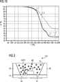
Es ist festzustellen, dass es optimale Verhältnisse gibt, sodass die thermische Stabilität zunächst zunimmt und bei zu hohem Anteil cyclischer Systeme wieder abnimmt oder sogar keine Aushärtung mehr beobachtet werden kann. Dies ist vermutlich darauf zurückzuführen, dass die Mobilität der bereits vernetzten Ketten abnimmt und somit nicht mehr alle reaktiven Gruppen einen Reaktionspartner finden. Sowohl freie Vinyl- als auch Hydridgruppen sind aber potentielle Schwachstellen der Polymere und sollten daher durch möglichst vollständige Vernetzung vermieden werden. Die in
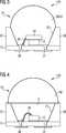
Die
Das Bauelement
Das optische Element
Die
Die
Die
Der Halbleiterchip
Die in Verbindung mit den Figuren beschriebenen Ausführungsbeispielen und deren Merkmale können gemäß weiterer Ausführungsbeispiele auch miteinander kombiniert werden, auch wenn solche Kombinationen nicht explizit in den Figuren gezeigt sind. Weiterhin können die in Verbindung mit den Figuren beschriebenen Ausführungsbeispiele zusätzliche oder alternative Merkmale gemäß der Beschreibung im allgemeinen Teil aufweisen.The embodiments described in connection with the figures and their features can also be combined with each other according to further embodiments, even if such combinations are not explicitly shown in the figures. Furthermore, the embodiments described in connection with the figures may have additional or alternative features as described in the general part.
Die Erfindung ist nicht durch die Beschreibung anhand der Ausführungsbeispiele auf diese beschränkt. Vielmehr umfasst die Erfindung jedes neue Merkmal sowie die Kombination von Merkmalen, was insbesondere jede Kombination von Merkmalen in den Patentansprüchen beinhaltet auch wenn dieses Merkmal oder diese Kombination selbst nicht explizit in den Patentansprüchen oder Ausführungsbeispielen angegeben ist.The invention is not limited by the description based on the embodiments of these. Rather, the invention includes any novel feature and the combination of features, which in particular includes any combination of features in the claims, even if this feature or combination itself is not explicitly stated in the claims or exemplary embodiments.
BezugszeichenlisteLIST OF REFERENCE NUMBERS
- 100100
- optoelektronisches Bauelement optoelectronic component
- 1010
- Halbleiterchip Semiconductor chip
- 1515
- Trägersubtrat Trägersubtrat
- 2020
- Gehäuse casing
- 2525
- Ausnehmung recess
- 3030
- erster Anschluss first connection
- 3131
- zweiter Anschluss second connection
- 3232
- Bonddraht bonding wire
- 5050
- optisches Element optical element
- 5151
- Verguss grouting
- 5252
- Reflektor reflector
- 6060
- Partikel oder Konvertermaterial Particle or converter material
- 6161
- Konversionselement conversion element
- 7070
- Linse lens
ZITATE ENTHALTEN IN DER BESCHREIBUNG QUOTES INCLUDE IN THE DESCRIPTION
Diese Liste der vom Anmelder aufgeführten Dokumente wurde automatisiert erzeugt und ist ausschließlich zur besseren Information des Lesers aufgenommen. Die Liste ist nicht Bestandteil der deutschen Patent- bzw. Gebrauchsmusteranmeldung. Das DPMA übernimmt keinerlei Haftung für etwaige Fehler oder Auslassungen.This list of the documents listed by the applicant has been generated automatically and is included solely for the better information of the reader. The list is not part of the German patent or utility model application. The DPMA assumes no liability for any errors or omissions.
Zitierte PatentliteraturCited patent literature
- EP 0905792 A2[0030]EP 0905792 A2[0030]
- WO 02/13281 A1[0030]WO 02/13281 A1[0030]
- WO 98/12757 A1[0035]WO 98/12757 A1[0035]
Claims (15)
Translated fromGerman


Priority Applications (5)
| Application Number | Priority Date | Filing Date | Title |
|---|---|---|---|
| DE102016115907.7ADE102016115907A1 (en) | 2016-08-26 | 2016-08-26 | Optoelectronic component and method for producing an optoelectronic component |
| JP2019508194AJP2019528349A (en) | 2016-08-26 | 2017-08-16 | Optoelectronic component and method for manufacturing the optoelectronic component |
| DE112017004289.5TDE112017004289A5 (en) | 2016-08-26 | 2017-08-16 | Optoelectronic component and method for producing an optoelectronic component |
| US16/328,680US10910531B2 (en) | 2016-08-26 | 2017-08-16 | Optoelectronic component and method for producing an optoelectronic component |
| PCT/EP2017/070780WO2018036883A1 (en) | 2016-08-26 | 2017-08-16 | Optoelectronic component and method for producing an optoelectronic component |
Applications Claiming Priority (1)
| Application Number | Priority Date | Filing Date | Title |
|---|---|---|---|
| DE102016115907.7ADE102016115907A1 (en) | 2016-08-26 | 2016-08-26 | Optoelectronic component and method for producing an optoelectronic component |
Publications (1)
| Publication Number | Publication Date |
|---|---|
| DE102016115907A1true DE102016115907A1 (en) | 2018-03-01 |
Family
ID=59738310
Family Applications (2)
| Application Number | Title | Priority Date | Filing Date |
|---|---|---|---|
| DE102016115907.7AWithdrawnDE102016115907A1 (en) | 2016-08-26 | 2016-08-26 | Optoelectronic component and method for producing an optoelectronic component |
| DE112017004289.5TWithdrawnDE112017004289A5 (en) | 2016-08-26 | 2017-08-16 | Optoelectronic component and method for producing an optoelectronic component |
Family Applications After (1)
| Application Number | Title | Priority Date | Filing Date |
|---|---|---|---|
| DE112017004289.5TWithdrawnDE112017004289A5 (en) | 2016-08-26 | 2017-08-16 | Optoelectronic component and method for producing an optoelectronic component |
Country Status (4)
| Country | Link |
|---|---|
| US (1) | US10910531B2 (en) |
| JP (1) | JP2019528349A (en) |
| DE (2) | DE102016115907A1 (en) |
| WO (1) | WO2018036883A1 (en) |
Citations (4)
| Publication number | Priority date | Publication date | Assignee | Title |
|---|---|---|---|---|
| WO1998012757A1 (en) | 1996-09-20 | 1998-03-26 | Siemens Aktiengesellschaft | Sealing material with wavelength converting effect, application and production process |
| EP0905792A2 (en) | 1997-09-30 | 1999-03-31 | Hewlett-Packard Company | Stacked-fringe integrated circuit capacitors |
| WO2002013281A1 (en) | 2000-08-08 | 2002-02-14 | Osram Opto Semiconductors Gmbh | Semiconductor chip for optoelectronics and method for production thereof |
| DE102012104363A1 (en)* | 2012-05-21 | 2013-11-21 | Osram Opto Semiconductors Gmbh | Optoelectronic component and method for its production |
Family Cites Families (15)
| Publication number | Priority date | Publication date | Assignee | Title |
|---|---|---|---|---|
| US6867323B2 (en)* | 2000-06-06 | 2005-03-15 | The Board Of Trustees Of The University Of Illinois | Cross-coupling reaction of organosilicon nucleophiles |
| WO2004016670A2 (en)* | 2002-08-16 | 2004-02-26 | The University Of Akron | Poly(cyclosiloxane) composiiton and method of synthesis thereof |
| JP4648099B2 (en)* | 2005-06-07 | 2011-03-09 | 信越化学工業株式会社 | Silicone resin composition for die bonding |
| US8629222B2 (en)* | 2008-03-28 | 2014-01-14 | Mitsubishi Chemical Corporation | Curable polysiloxane composition, and polysiloxane cured product, optical member, member for aerospace industry, semiconductor light-emitting device, illuminating device and image display device using the same |
| JP2010202801A (en)* | 2009-03-04 | 2010-09-16 | Nitto Denko Corp | Composition for thermosetting silicone resin |
| US9299896B2 (en)* | 2010-01-25 | 2016-03-29 | Lg Chem, Ltd. | Curable composition |
| JP6116912B2 (en)* | 2010-02-19 | 2017-04-19 | ボード・オブ・リージエンツ,ザ・ユニバーシテイ・オブ・テキサス・システム | Branched siloxanes and methods for synthesis |
| WO2011155459A1 (en)* | 2010-06-11 | 2011-12-15 | 株式会社Adeka | Silicon-containing curable composition, cured product of the silicon-containing curable composition and lead frame substrate formed of the silicon-containing curable composition |
| US20120029157A1 (en)* | 2010-07-29 | 2012-02-02 | Woo-Han Kim | Modified siloxane polymer composition, encapsulant obtained from the modified siloxane polymer composition, and electronic device including the encapsulant |
| JP2012162704A (en) | 2010-07-29 | 2012-08-30 | Cheil Industries Inc | Modified siloxane polymer composition, encapsulant obtained from the modified siloxane polymer composition, and electronic device including the encapsulant |
| DE102010062244A1 (en)* | 2010-12-01 | 2012-06-06 | Evonik Goldschmidt Gmbh | Process for the reaction of hydroxy compounds with linear, branched or cyclic polyalkysiloxanes |
| WO2013052181A2 (en)* | 2011-06-17 | 2013-04-11 | Ndsu Research Foundation | Functionalized silicones with polyalkylene oxide side chains |
| JP6043292B2 (en)* | 2011-10-04 | 2016-12-14 | 株式会社カネカ | Curable resin composition, curable resin composition tablet, molded product, semiconductor package, semiconductor component, and light emitting diode |
| KR101518497B1 (en) | 2012-06-12 | 2015-05-11 | 제일모직주식회사 | Composite sheet, method for preparing thereof and display substrate comprising the same |
| US20150038220A1 (en)* | 2013-05-31 | 2015-02-05 | Yury Kuznetsov | On-line picture/video voting |
- 2016
- 2016-08-26DEDE102016115907.7Apatent/DE102016115907A1/ennot_activeWithdrawn
- 2017
- 2017-08-16DEDE112017004289.5Tpatent/DE112017004289A5/ennot_activeWithdrawn
- 2017-08-16USUS16/328,680patent/US10910531B2/ennot_activeExpired - Fee Related
- 2017-08-16WOPCT/EP2017/070780patent/WO2018036883A1/ennot_activeCeased
- 2017-08-16JPJP2019508194Apatent/JP2019528349A/enactivePending
Patent Citations (4)
| Publication number | Priority date | Publication date | Assignee | Title |
|---|---|---|---|---|
| WO1998012757A1 (en) | 1996-09-20 | 1998-03-26 | Siemens Aktiengesellschaft | Sealing material with wavelength converting effect, application and production process |
| EP0905792A2 (en) | 1997-09-30 | 1999-03-31 | Hewlett-Packard Company | Stacked-fringe integrated circuit capacitors |
| WO2002013281A1 (en) | 2000-08-08 | 2002-02-14 | Osram Opto Semiconductors Gmbh | Semiconductor chip for optoelectronics and method for production thereof |
| DE102012104363A1 (en)* | 2012-05-21 | 2013-11-21 | Osram Opto Semiconductors Gmbh | Optoelectronic component and method for its production |
Also Published As
| Publication number | Publication date |
|---|---|
| DE112017004289A5 (en) | 2019-05-29 |
| JP2019528349A (en) | 2019-10-10 |
| WO2018036883A8 (en) | 2018-06-14 |
| WO2018036883A1 (en) | 2018-03-01 |
| US20190207067A1 (en) | 2019-07-04 |
| US10910531B2 (en) | 2021-02-02 |
Similar Documents
| Publication | Publication Date | Title |
|---|---|---|
| CN105358615B (en) | Additives for Silicone Encapsulation Materials | |
| DE112017002058B4 (en) | Method for producing an optoelectronic component and optoelectronic component | |
| DE102012104363A1 (en) | Optoelectronic component and method for its production | |
| KR101560030B1 (en) | Curable composition | |
| WO2014100652A1 (en) | Layered polymer structures and methods | |
| KR20110068867A (en) | Resin composition for optical semiconductor element sealing and optical semiconductor device sealed with the said composition | |
| DE202011110489U1 (en) | Curable composition | |
| KR20130084997A (en) | Uv curable adhesive silicone composition, uv curable adhesive silicone composition sheet, optical semiconductor device and method for producing the same | |
| DE202011110490U1 (en) | silicone resin | |
| KR101560046B1 (en) | Curable composition | |
| KR101030019B1 (en) | Translucent resin for encapsulant and electronic device comprising same | |
| DE102014223785A1 (en) | Curable, highly transparent silicone composition with improved optical component mechanics | |
| TWI873237B (en) | Curable white organic silicon composition, reflective material for optical semiconductor device, and optical semiconductor device | |
| DE102021120040A1 (en) | HEAT CURING SILICONE COMPOSITION | |
| DE112015001546T5 (en) | Wavelength conversion compositions, wavelength converters and devices therewith | |
| DE102021118751A1 (en) | CURABLE SILICONE COMPOSITION, ENCAPSULING AGENT AND OPTICAL SEMICONDUCTOR DEVICE | |
| DE102021118377A1 (en) | CURABLE SILICONE COMPOSITION, ENCAPSULING AGENT AND OPTICAL SEMICONDUCTOR DEVICE | |
| KR101169031B1 (en) | Thermosetting Silicone Composition for Light Emitting Diode Encapsulant | |
| DE102004039111A1 (en) | Curable silicone resin composition | |
| US11370917B2 (en) | Curable hotmelt silicone composition, encapsulant, film and optical semiconductor device | |
| DE102016115907A1 (en) | Optoelectronic component and method for producing an optoelectronic component | |
| KR20210082358A (en) | Curable white silicone formulation, a reflective material for optical semiconductor module and optical semiconductor device | |
| DE112020002326T5 (en) | OPTOELECTRONIC DEVICE AND METHOD FOR MANUFACTURING OPTOELECTRONIC DEVICE | |
| DE102013112826B4 (en) | Optoelectronic component comprising an adhesive layer and a method for producing an adhesive layer in an optoelectronic component | |
| JP2016531988A (en) | Additive for silicone sealant |
Legal Events
| Date | Code | Title | Description |
|---|---|---|---|
| R163 | Identified publications notified | ||
| R118 | Application deemed withdrawn due to claim for domestic priority |