DE102016105454A1 - Organic light-emitting device, method of manufacturing an organic light-emitting device, and method of operating an organic light-emitting device - Google Patents
Organic light-emitting device, method of manufacturing an organic light-emitting device, and method of operating an organic light-emitting deviceDownload PDFInfo
- Publication number
- DE102016105454A1 DE102016105454A1DE102016105454.2ADE102016105454ADE102016105454A1DE 102016105454 A1DE102016105454 A1DE 102016105454A1DE 102016105454 ADE102016105454 ADE 102016105454ADE 102016105454 A1DE102016105454 A1DE 102016105454A1
- Authority
- DE
- Germany
- Prior art keywords
- antenna
- organic light
- electrode
- layer structure
- emitting component
- Prior art date
- Legal status (The legal status is an assumption and is not a legal conclusion. Google has not performed a legal analysis and makes no representation as to the accuracy of the status listed.)
- Pending
Links
Images

Classifications
- H—ELECTRICITY
- H10—SEMICONDUCTOR DEVICES; ELECTRIC SOLID-STATE DEVICES NOT OTHERWISE PROVIDED FOR
- H10K—ORGANIC ELECTRIC SOLID-STATE DEVICES
- H10K50/00—Organic light-emitting devices
- H10K50/80—Constructional details
- H10K50/805—Electrodes
- H10K50/81—Anodes
- H10K50/814—Anodes combined with auxiliary electrodes, e.g. ITO layer combined with metal lines
- H—ELECTRICITY
- H10—SEMICONDUCTOR DEVICES; ELECTRIC SOLID-STATE DEVICES NOT OTHERWISE PROVIDED FOR
- H10K—ORGANIC ELECTRIC SOLID-STATE DEVICES
- H10K50/00—Organic light-emitting devices
- H10K50/80—Constructional details
- H10K50/805—Electrodes
- H10K50/81—Anodes
- H10K50/816—Multilayers, e.g. transparent multilayers
- H—ELECTRICITY
- H10—SEMICONDUCTOR DEVICES; ELECTRIC SOLID-STATE DEVICES NOT OTHERWISE PROVIDED FOR
- H10K—ORGANIC ELECTRIC SOLID-STATE DEVICES
- H10K59/00—Integrated devices, or assemblies of multiple devices, comprising at least one organic light-emitting element covered by group H10K50/00
Landscapes
- Physics & Mathematics (AREA)
- Optics & Photonics (AREA)
- Electroluminescent Light Sources (AREA)
Abstract
Translated fromGermanDescription
Translated fromGermanDie Erfindung betrifft ein organisches lichtemittierendes Bauelement, ein Verfahren zum Herstellen eines organischen lichtemittierenden Bauelements und ein Verfahren zum Betreiben eines organischen lichtemittierenden Bauelements.The invention relates to an organic light-emitting component, to a method for producing an organic light-emitting component and to a method for operating an organic light-emitting component.
Lichtemittierende Bauelemente auf organischer Basis, sogenannte organische lichtemittierende Bauelemente, finden zunehmend verbreitete Anwendung. Beispielsweise halten organische Leuchtdioden (organic light emitting diode – OLED) zunehmend Einzug in die Allgemeinbeleuchtung, beispielsweise als Flächenlichtquellen.Organic-based light-emitting components, so-called organic light-emitting components, are finding increasing widespread use. For example, organic light-emitting diodes (organic light-emitting diode (OLED) are increasingly being used in general lighting, for example as area light sources.
Ein organisches lichtemittierendes Bauelement, beispielsweise eine OLED, kann eine Anode und eine Kathode und dazwischen ein organisches funktionelles Schichtensystem aufweisen. Das organische funktionelle Schichtensystem kann aufweisen eine oder mehrere Emitterschichten, in denen elektromagnetische Strahlung erzeugt wird, eine Ladungsträgerpaar-Erzeugungs-Schichtenstruktur aus jeweils zwei oder mehr Ladungsträgerpaar-Erzeugungs-Schichten („charge generating layer“, CGL) zur Ladungsträgerpaarerzeugung, sowie eine oder mehrere Elektronenblockadeschichten, auch bezeichnet als Lochtransportschichten („hole transport layer“ – HTL), und eine oder mehrere Lochblockadeschichten, auch bezeichnet als Elektronentransportschichten („electron transport layer“ – ETL), um den Stromfluss zu richten.An organic light-emitting device, such as an OLED, may include an anode and a cathode and an organic functional layer system therebetween. The organic functional layer system may comprise one or more emitter layers in which electromagnetic radiation is generated, a charge carrier pair generation layer structure each consisting of two or more charge generating layers (CGL) for charge carrier pair generation, and one or more Electron block layers, also referred to as hole transport layers (HTL), and one or more hole block layers, also referred to as electron transport layers (ETLs), for directing the flow of current.
Bisher unabhängig davon werden für eine Positionsermittlung in einem Gebäude, beispielsweise für eine GPS-freie Navigation in geschlossenen Räumen, beispielsweise in einem Kaufhaus, in einem Parkhaus, in einer U-Bahn-Station, in einem Museum, in einem Industriegebäude und/oder einer Lagerhalle festinstallierte Funksender benötigt. Diese Funksender senden regelmäßig eine Identifikationsnummer (ID) in Form eines Funksignals, üblicherweise im GHz-Bereich, aus. Dieses Signal kann von Handheldgeräten, beispielsweise Smartphones, Tablets, Smartwatches und/oder Robotern oder Drohnen zur Positionsbestimmung genutzt werden.So far, regardless of this, for a position determination in a building, for example, for a GPS-free navigation in closed spaces, for example in a department store, in a parking garage, in a subway station, in a museum, in an industrial building and / or a Warehouse permanently installed radio transmitter needed. These radio transmitters regularly send out an identification number (ID) in the form of a radio signal, usually in the GHz range. This signal can be used by handheld devices, such as smartphones, tablets, smartwatches, and / or robots or drones for position determination.
Derartige Funksender werden heutzutage auch als Beacons bezeichnet. Beacons sind in der Regel batteriebetriebene Funksender, die beispielsweise ein Bluetooth-Signal aussenden. Es ist bekannt, zusätzlich zu Lampen Beacons in Leuchten anzuordnen, die zum Beleuchten des entsprechenden Gebäudes, insbesondere Raumes, verwendet werden. In diesem Fall kann das entsprechende Beacon die Stromversorgung der entsprechenden Leuchte verwenden und benötigt keine Batterie. Das Wort Beacon leitet sich von dem englischen Begriff für ‚Leuchtfeuer‘ ab und ist ein Hinweis auf das Funktionsprinzip. Beacons basieren auf einem Sender-Empfänger-Prinzip. Dazu werden im Raum mehrere Beacons als Signalgeber platziert, die in festen Zeitintervallen Signale senden. Kommt ein Empfänger, beispielsweise ein Smartphone mit einer installierten Mobile App, die für den Empfang von iBeacon Signalen konfiguriert ist, in die Reichweite eines Beacons, kann die ID des Senders identifiziert und seine Signalstärke gemessen werden. Sind mindestens drei Beacons in Reichweite des Endgeräts, lässt sich, beispielsweise durch Trilateration oder das Fingerprinting-Verfahren, die Position des Empfängers im zweidimensionalen Raum errechnen. Zur Ermittlung eines Standortes in einem dreidimensionalen Raum sind vier Beacons in Reichweite erforderlich.Such radio transmitters are now also referred to as beacons. Beacons are usually battery-operated radio transmitters that emit a Bluetooth signal, for example. It is known to arrange in addition to lamps beacons in lights that are used to illuminate the corresponding building, in particular room. In this case, the corresponding beacon can use the power supply of the corresponding lamp and does not require a battery. The word beacon is derived from the English term for 'beacon' and is an indication of the principle of operation. Beacons are based on a transmitter-receiver principle. For this purpose, several beacons are placed in the room as signal transmitters, which send signals at fixed time intervals. If a receiver, for example a smartphone with an installed mobile app configured to receive iBeacon signals, is within the range of a beacon, the ID of the transmitter can be identified and its signal strength can be measured. If at least three beacons are within range of the end device, the position of the receiver in two-dimensional space can be calculated, for example by trilateration or the fingerprinting method. Determining a location in a three-dimensional space requires four beacons within range.
Bereits bei der Raumplanung werden Leuchten nach Architekturrastern angeordnet und so werden definierte Positionen mit entsprechenden Beacons ausgestattet. Bei herkömmlichen Leuchten werden die Funkelemente der Beacons im Gehäuseinneren der entsprechenden Leuchte versteckt. Zur Vermeidung einer Abschirmung des Funksignals werden dafür Kunststoffgehäuse verwendet oder, im Falle eines Metallgehäuses, werden die Antennen der Beacons aus dem Metallgehäuse herausgeführt.Already during the spatial planning, luminaires are arranged according to architectural buttons and thus defined positions are equipped with corresponding beacons. In conventional luminaires, the radio elements of the beacons are hidden inside the housing of the corresponding luminaire. To avoid a shielding of the radio signal for plastic housing are used or, in the case of a metal housing, the antennas of the beacons are led out of the metal housing.
Das Ausbilden der Beacons, das Anordnen der Beacons in den Gehäusen der Leuchten und/oder das Herausführen der Antennen der Beacons aus den Gehäusen ist in der Regel sehr kostenintensiv und/oder zeitaufwendig.Forming the beacons, arranging the beacons in the housings of the luminaires and / or removing the antennas of the beacons from the housings is usually very cost-intensive and / or time-consuming.
Eine Aufgabe der Erfindung ist es, ein organisches lichtemittierendes Bauelement bereitzustellen, das einen Funksender und/oder einen Funkempfänger aufweist und das einfach, schnell und/oder kostengünstig herstellbar ist.An object of the invention is to provide an organic light-emitting component which has a radio transmitter and / or a radio receiver and which is simple, quick and / or inexpensive to produce.
Eine Aufgabe der Erfindung ist es, ein Verfahren zum Herstellen eines organischen lichtemittierenden Bauelements, das einen Funksender und/oder einen Funkempfänger aufweist, bereitzustellen, das einfach, schnell und/oder kostengünstig durchführbar ist.An object of the invention is to provide a method for producing an organic light-emitting component which has a radio transmitter and / or a radio receiver, which is simple, quick and / or cost-effective to carry out.
Eine Aufgabe der Erfindung ist es, ein Verfahren zum Betreiben eines organischen lichtemittierenden Bauelements, das einen Funksender und/oder einen Funkempfänger aufweist, bereitzustellen, das auf einfache und/oder kostengünstige Weise ein zuverlässiges Senden bzw. Empfangen von Informationen ermöglicht.An object of the invention is to provide a method of operating an organic light-emitting device comprising a radio transmitter and / or a radio receiver, which enables a reliable and / or cost-effective way of reliably transmitting or receiving information.
Eine Aufgabe der Erfindung wird gelöst durch ein organisches lichtemittierendes Bauelement, mit: einer Metallschichtenstruktur, die eine erste Elektrode und eine Antenne aufweist; einer organischen funktionellen Schichtenstruktur über der ersten Elektrode; einer zweiten Elektrode über der organischen funktionellen Schichtenstruktur; und einem elektronischen Schaltkreis, der zumindest mit der Antenne elektrisch gekoppelt ist und der dazu eingerichtet ist, im Betrieb des organischen lichtemittierenden Bauelements ein erstes elektrisches Signal an die Antenne anzulegen, so dass die Antenne ein dazu korrespondierendes erstes elektromagnetisches Signal abstrahlt, und/oder von der Antenne ein zweites elektrisches Signal zu empfangen, welches aufgrund eines von der Antenne empfangenen zweiten elektromagnetischen Signals erzeugt wird.An object of the invention is achieved by an organic light emitting device, comprising: a metal layer structure having a first electrode and an antenna; an organic functional layer structure over the first electrode; a second electrode over the organic functional layer structure; and an electronic circuit which is electrically coupled at least to the antenna and which is adapted to apply a first electrical signal to the antenna during operation of the organic light-emitting component, so that the antenna emits a first electromagnetic signal corresponding thereto, and / or the antenna to receive a second electrical signal which is generated due to a second electromagnetic signal received by the antenna.
Die Antenne besteht aus einem oder mehreren aktiven oder passiven Antennenelementen, beispielsweise parasitären Antennenelementen. Die Länge der Antenne, insbesondere der Antennenelemente, und/oder Abstände der Antennenelemente zueinander sind abhängig vom gewünschten Sende- und/oder Empfangs-Frequenzbereich. Beispielsweise kann zum Senden und/oder Empfangen im 2,4 GHz Bereich, beispielsweise im Bluetooth-Bereich, eine Länge der Antenne und/oder der Antennenelemente ca. 5 cm sein. Die Metallschichtenstruktur, insbesondere die Antenne, insbesondere die Antennenelemente, besteht aus einem leitfähigen Material, beispielsweise ITO, PEDOT:PSS, CrAlCr, Ag, Cu, Au. Die Metallschichtenstruktur ist eine lateral strukturierte Fläche, wobei die Antenne und die erste Elektrode von den lateralen Strukturen gebildet sind. Für die Einspeisung oder auch Auskopplung des Signals, beispielsweise eines HF-Signals, ist die Antenne, insbesondere die Antennenelemente, mit einem oder mehreren Anschlusselementen des elektronischen Schaltkreises verbunden. Die Antenne kann beispielsweise in Form einer Yagi-Antenne /oder in Form einer logarithmisch-periodischen Antenne ausgebildet sein.The antenna consists of one or more active or passive antenna elements, for example parasitic antenna elements. The length of the antenna, in particular of the antenna elements, and / or distances of the antenna elements from one another depend on the desired transmission and / or reception frequency range. For example, for transmission and / or reception in the 2.4 GHz range, for example in the Bluetooth range, a length of the antenna and / or of the antenna elements may be approximately 5 cm. The metal layer structure, in particular the antenna, in particular the antenna elements, consists of a conductive material, for example ITO, PEDOT: PSS, CrAlCr, Ag, Cu, Au. The metal layer structure is a laterally structured surface, wherein the antenna and the first electrode are formed by the lateral structures. For the supply or also decoupling of the signal, for example an RF signal, the antenna, in particular the antenna elements, is connected to one or more connection elements of the electronic circuit. The antenna can be designed, for example, in the form of a Yagi antenna or in the form of a logarithmic periodic antenna.
Das organische lichtemittierende Bauelement, im Folgenden auch kurz OLED genannt, ist eine Lampe und/oder eine Leuchtmittel, das in einer Leuchte, beispielsweise einer Deckenleuchte, einer Wandleuchte und/oder einer Standleuchte, angeordnet werden kann.The organic light-emitting component, also referred to below as OLED for short, is a lamp and / or a luminous means which can be arranged in a lamp, for example a ceiling lamp, a wall lamp and / or a floor lamp.
Das Integrieren der Antenne in den Schichtenaufbau der OLED und damit das Integrieren der Antenne direkt in die Lampe bzw. das Leuchtmittel bewirken zum Einen, dass die Antenne immer an der Vorderseite und/oder an einer nach außen offenen Seite eines Gehäuses der Leuchte, in der die OLED angeordnet ist, angeordnet ist, da Lampen bzw. Leuchtmittel grundsätzlich an einer nach außen geöffneten Stelle der Gehäuse der Leuchten angeordnet sind, damit das Licht, das von der entsprechenden Lampe bzw. dem entsprechenden Leuchtmittel erzeugt wird, nach außen abgestrahlt werden kann. Diese Positionierung der Antenne ist besonders günstig, da nur eine besonders geringe, vernachlässigbare oder gar keine elektromagnetische Abschirmung des Signals durch das Gehäuse der Leuchte erfolgt. Dies ermöglicht, ein Metallgehäuse für die entsprechende Leuchte verwenden zu können, ohne die Antenne aus dem Metallgehäuse herausführen zu müssen. Außerdem trägt dies dazu bei, dass die Sende- und/oder Empfangsleistung grundsätzlich besonders gut ist. Dies trägt dazu bei, dass über die Antenne Informationen mit einem besonders geringen Energieaufwand zuverlässig empfangbar ausgestrahlt werden können oder mit einer besonders hohen Genauigkeit abgestrahlt oder empfangen werden können.The integration of the antenna in the layer structure of the OLED and thus the integration of the antenna directly into the lamp or the illuminant cause on the one hand, that the antenna always on the front and / or on an outwardly open side of a housing of the lamp, in the the OLED is arranged, since lamps or lamps are basically arranged at an outwardly open position of the housing of the luminaires, so that the light generated by the corresponding lamp or the corresponding lamp can be radiated to the outside. This positioning of the antenna is particularly favorable, since only a particularly small, negligible or no electromagnetic shielding of the signal takes place through the housing of the lamp. This makes it possible to use a metal housing for the corresponding lamp without having to lead the antenna out of the metal housing. In addition, this contributes to the fact that the transmission and / or reception power is in principle very good. This contributes to the fact that information with a particularly low energy consumption can be transmitted reliably receivable via the antenna or can be emitted or received with a particularly high accuracy.
Das Integrieren der Antenne in den Schichtenaufbau der OLED und damit das Integrieren der Antenne direkt in die Lampe bzw. das Leuchtmittel bewirken zum Anderen, dass der Herstellaufwand und die Herstellkosten besonders gering gehalten werden können, da die Antenne und die entsprechenden lateralen Strukturen der Metallschichtenstruktur in denselben Prozessschritten hergestellt werden können wie andere Strukturen der OLED, beispielsweise die erste Elektrode, Kontaktabschnitte der OLED oder Stromverteilerelemente, beispielsweise Busbars, der OLED.Integrating the antenna into the layer structure of the OLED and thus integrating the antenna directly into the lamp or the luminous means, on the other hand, can minimize the manufacturing outlay and the production costs, since the antenna and the corresponding lateral structures of the metal layer structure in FIG the same process steps can be made as other structures of the OLED, for example, the first electrode, contact portions of the OLED or power distribution elements, such as busbars, the OLED.
Zusätzlich zu der Antenne können ein, zwei oder mehr weitere Antennen in den Schichtenaufbau der OLED integriert werden. Alternativ oder zusätzlich können in die Antenne bzw. die Antennen jeweils ein, zwei oder mehr Antennenelemente aufweisen. Die Antenne bzw. die Antennenelemente können so zusammengeschaltet werden, dass dies zu einer Verbesserung der Abstrahlrichtung und der Empfangsverbesserung führt. Alternativ kann dadurch die Sendeleistung reduziert werden, wodurch Energie gespart werden kann und/oder Elektrosmog reduziert werden kann. Ferner könnte ein Ausfall einer Antenne bzw. eines Antennenelements durch die Redundanz aufgrund der anderen Antennen bzw. Antennenelemente kompensiert werden.In addition to the antenna, one, two or more further antennas can be integrated into the layer structure of the OLED. Alternatively or additionally, one, two or more antenna elements can each have in the antenna or the antennas. The antenna or the antenna elements can be interconnected so that this leads to an improvement of the emission direction and the reception improvement. Alternatively, the transmission power can thereby be reduced, whereby energy can be saved and / or electrosmog can be reduced. Furthermore, a failure of an antenna or an antenna element could be compensated by the redundancy due to the other antennas or antenna elements.
Gemäß einer Weiterbildung ist die Antenne lateral neben der ersten Elektrode ausgebildet. Die erste Elektrode, die organische funktionelle Schichtenstruktur und die zweite Elektrode definieren in dem Bereich, in dem sie sich in lateraler Richtung überlappen, im Betrieb der OLED eine Leuchtfläche der OLED. Das Anordnen der Antenne lateral neben der ersten Elektrode bewirkt, dass die Antenne außerhalb der Leuchtfläche angeordnet ist. In anderen Worten ist die leitfähige Struktur der Antenne nicht in dem leuchtenden Bereich der OLED, die beispielsweise als Flächenlichtquelle ausgebildet ist, angeordnet. Dies ermöglicht, dass für die Antenne ein Material gewählt werden kann, das nicht transparent oder nicht transluzent ist. Optional kann jedoch auch ein transparentes oder transluzent das Material für die Antenne gewählt werden. According to a development, the antenna is formed laterally next to the first electrode. The first electrode, the organic functional layer structure and the second electrode define a luminous area of the OLED in the region in which they overlap in the lateral direction during operation of the OLED. Arranging the antenna laterally adjacent to the first electrode causes the antenna to be located outside the luminous area. In other words, the conductive structure of the antenna is not arranged in the luminous region of the OLED, which is formed for example as a surface light source. This allows the antenna to select a material that is not transparent or translucent. Optionally, however, a transparent or translucent material for the antenna can be selected.
Gemäß einer Weiterbildung ist die Antenne gegenüber der ersten Elektrode elektrisch isoliert. Dies bewirkt, dass das erste Signal, das mittels der Antenne abgestrahlt wird, oder das zweite Signal, das mittels der Antenne empfangen wird, nicht von einem Strom oder einer Spannung beeinflusst wird, der im Leuchtbetrieb der OLED über die erste Elektrode fließt bzw. die im Leuchtbetrieb der OLED an der ersten Elektrode anliegt.According to a development, the antenna is electrically insulated from the first electrode. This causes the first signal, which is radiated by means of the antenna, or the second signal, which is received by means of the antenna, not to be influenced by a current or a voltage which flows in the lighting operation of the OLED via the first electrode is in lighting operation of the OLED at the first electrode.
Gemäß einer Weiterbildung ist die Antenne vertikal über oder unter der ersten Elektrode ausgebildet. Anschaulich gesprochen ist die Antenne innerhalb der Leuchtfläche der OLED angeordnet. Dies kann dazu beitragen, dass eine Abschirmung der Antenne aufgrund anderer Materialien der OLED oder aufgrund eines Gehäuses einer Leuchte, in der die OLED angeordnet ist, besonders gering ist, da die Leuchtfläche eines Leuchtmittels in einer Leuchte grundsätzlich nicht oder nur möglichst wenig abgeschirmt wird. Ferner kann dies einen relativ großen Spielraum bei der Wahl der Größe und/oder der Form der Antenne bieten, da die Leuchtflächen von OLEDs grundsätzlich relativ groß sind und da daher im Bereich der Leuchtfläche ausreichend Platz für verschiedene Größen und/oder Formen der Antenne ist. Ferner ermöglicht dies, die Antenne zum Verteilen eines Stroms zu verwenden, der zum Erzeugen des Leuchtbetriebs der OLED verwendet wird.According to a development, the antenna is formed vertically above or below the first electrode. Illustratively speaking, the antenna is arranged within the luminous area of the OLED. This can contribute to a shielding of the antenna due to other materials of the OLED or due to a housing of a luminaire in which the OLED is arranged, is particularly low, since the luminous surface of a lamp in a lamp is not shielded or shielded as little as possible. Furthermore, this can offer a relatively large margin in the choice of the size and / or the shape of the antenna, since the luminous surfaces of OLEDs are basically relatively large and therefore there is sufficient space in the region of the luminous area for different sizes and / or shapes of the antenna. Further, this makes it possible to use the antenna for distributing a current used for generating the lighting operation of the OLED.
Gemäß einer Weiterbildung ist die Antenne in direkten körperlichen Kontakt mit der ersten Elektrode. In anderen Worten befinden sich die leitfähigen lateralen Strukturen der Antenne in direkten körperlichen Kontakt mit der ersten Elektrode innerhalb der Leuchtfläche. Dies bewirkt, dass ein Strom, der über die erste Elektrode fließt, auch über die Antenne fließt und die Antenne somit zum Leiten und/oder Verteilen des Stroms über die Leuchtfläche beiträgt.According to a development, the antenna is in direct physical contact with the first electrode. In other words, the conductive lateral structures of the antenna are in direct physical contact with the first electrode within the luminous area. This causes a current flowing across the first electrode to also flow across the antenna, thus contributing to the conduction and / or distribution of the current across the light area.
Gemäß einer Weiterbildung ist die Antenne vertikal über oder unter der zweiten Elektrode ausgebildet. Anschaulich gesprochen ist die Antenne innerhalb der Leuchtfläche der OLED angeordnet. Dies kann dazu beitragen, dass eine Abschirmung der Antenne aufgrund anderer Materialien der OLED oder aufgrund eines Gehäuses einer Leuchte, in der die OLED angeordnet ist, besonders gering ist, da die Leuchtfläche eines Leuchtmittels in einer Leuchte grundsätzlich nicht oder nur möglichst wenig abgeschirmt wird. Ferner kann dies einen relativ großen Spielraum bei der Wahl der Größe und/oder der Form der Antenne bieten, da die Leuchtflächen von OLEDs grundsätzlich relativ groß sind und da daher im Bereich der Leuchtfläche ausreichend Platz für verschiedene Größen und/oder Formen der Antenne ist. Ferner ermöglicht dies, die Antenne zum Verteilen eines Stroms zu verwenden, der zum Erzeugen des Leuchtbetriebs der OLED verwendet wird.According to a development, the antenna is formed vertically above or below the second electrode. Illustratively speaking, the antenna is arranged within the luminous area of the OLED. This can contribute to a shielding of the antenna due to other materials of the OLED or due to a housing of a luminaire in which the OLED is arranged, is particularly low, since the luminous surface of a lamp in a lamp is not shielded or shielded as little as possible. Furthermore, this can offer a relatively large margin in the choice of the size and / or the shape of the antenna, since the luminous surfaces of OLEDs are basically relatively large and therefore there is sufficient space in the region of the luminous area for different sizes and / or shapes of the antenna. Further, this makes it possible to use the antenna for distributing a current used for generating the lighting operation of the OLED.
Gemäß einer Weiterbildung ist die Antenne in direkten körperlichen Kontakt mit der zweiten Elektrode. In anderen Worten befinden sich die leitfähigen lateralen Strukturen der Antenne in direkten körperlichen Kontakt mit der zweiten Elektrode innerhalb der Leuchtfläche. Dies bewirkt, dass ein Strom, der über die zweite Elektrode fließt, auch über die Antenne fließt und die Antenne somit zum Leiten und/oder Verteilen des Stroms über die Leuchtfläche beiträgt.According to a development, the antenna is in direct physical contact with the second electrode. In other words, the conductive lateral structures of the antenna are in direct physical contact with the second electrode within the luminous area. This causes a current that flows through the second electrode to also flow via the antenna, and thus the antenna contributes to conducting and / or distributing the current across the luminous area.
Gemäß einer Weiterbildung dient die Antenne als Stromverteilungsstruktur zum gleichmäßigen Verteilen von Strom über die erste Elektrode bzw. die zweite Elektrode. Die lateralen Strukturen der Antenne dienen somit sowohl zum Senden und/oder Empfangen von Informationen, insbesondere Daten, als auch zur Stromverteilung, beispielsweise Stromaufweitung. Die Antenne kann in diesem Zusammenhang auch als Stromverteilungselement oder Busbar bezeichnet werden und/oder ausgebildet sein. Eine Trennung des für die Lichtfunktion verwendeten Stroms, beispielsweise eines Gleichstroms, und des ersten bzw. zweiten Signals, das beispielsweise im HF-Bereich liegen kann, erfolgt durch den elektronischen Schaltkreis. Das System aus Leuchtmittel und Sende- bzw. Empfangsmittel wird dann mit einem modulierten elektrischen Signal betrieben.According to a development, the antenna serves as a current distribution structure for the uniform distribution of current through the first electrode or the second electrode. The lateral structures of the antenna thus serve both for transmitting and / or receiving information, in particular data, as well as for power distribution, for example current spreading. The antenna may also be referred to as power distribution element or busbar in this context and / or be formed. A separation of the current used for the light function, for example a direct current, and the first and second signal, which may for example be in the RF range, is performed by the electronic circuit. The system of lighting means and transmitting and receiving means is then operated with a modulated electrical signal.
Gemäß einer Weiterbildung ist die Antenne in die organische funktionelle Schichtenstruktur eingebettet. In anderen Worten ist die Antenne in zwei oder drei Raumrichtungen von dem Material der organischen funktionellen Schichtenstruktur umgeben. Optional kann zwischen der Antenne und dem Material der organischen funktionellen Schichtenstruktur ein elektrisch isolierendes Material, beispielsweise eine elektrisch isolierender Lack, ausgebildet sein.According to a development, the antenna is embedded in the organic functional layer structure. In other words, the antenna is surrounded in two or three spatial directions by the material of the organic functional layer structure. Optionally, an electrically insulating material, for example an electrically insulating lacquer, may be formed between the antenna and the material of the organic functional layer structure.
Gemäß einer Weiterbildung ist die Antenne zum Senden und/oder Empfangen von Frequenzen im GHz-Bereich ausgebildet. Beispielsweise weisen die Antenne und/oder Antennenelemente der Antenne jeweils eine Länge von ungefähr 5 cm auf. Alternativ dazu können Frequenzen im Generation 5 Mobilfunknetz gesendet und/oder empfangen werden, beispielsweise zwischen 6000 Mhz und 18000 Mhz, beispielsweise mit einer Länge der Antenne und/oder der Antennenelemente von 0,4 cm bis 1,5 cm. Alternativ dazu können Frequenzen im WLAN-Bereich empfangen und/oder gesendet werden, beispielsweise zwischen 2400 Mhz und 5000 Mhz, beispielsweise mit einer Länge der Antenne und/oder der Antennenelemente von 1,4 cm bis 14 cm. Alternativ dazu können Frequenzen im Funkbeacon-Bereich empfangen und/oder gesendet werden, beispielsweise bei ungefähr 2400 Mhz, beispielsweise mit einer Länge der Antenne und/oder der Antennenelemente von ungefähr 3 cm. Alternativ dazu können Frequenzen im Generation 4 Mobilfunknetz (LTE) empfangen und/oder gesendet werden, beispielsweise bei ungefähr 2100 Mhz, beispielsweise mit einer Länge der Antenne und/oder der Antennenelemente von 3 cm bis 20 cm.According to a development, the antenna is designed for transmitting and / or receiving frequencies in the GHz range. For example, the antenna and / or antenna elements of the antenna each have a length of about 5 cm. Alternatively, frequencies in the generation 5 mobile network can be transmitted and / or received, for example between 6000 MHz and 18000 MHz, for example with a length of the antenna and / or the antenna elements of 0.4 cm to 1.5 cm. Alternatively, frequencies in the WLAN area may be received and / or transmitted, for example between 2400 MHz and 5000 MHz, for example with a length of the antenna and / or the antenna elements of 1.4 cm to 14 cm. Alternatively, frequencies in the radio beacon range may be received and / or transmitted, for example at approximately 2400 MHz, for example with a length of the antenna and / or antenna elements of approximately 3 cm. Alternatively, frequencies in the Generation 4 Mobile Network (LTE) may be received and / or transmitted, for example at approximately 2100 MHz, for example with a length of the antenna and / or the antenna elements of 3 cm to 20 cm.
Eine Aufgabe der Erfindung wird gelöst durch ein Verfahren zum Herstellen des organischen lichtemittierenden Bauelements, bei dem: die Metallschichtenstruktur, die die erste Elektrode und die Antenne aufweist, ausgebildet wird; die organische funktionelle Schichtenstruktur über der ersten Elektrode ausgebildet wird; die zweite Elektrode über der organischen funktionellen Schichtenstruktur ausgebildet wird; der elektronische Schaltkreis mit der Antenne elektrisch gekoppelt wird und dazu ausgebildet wird, im Betrieb des organischen lichtemittierenden Bauelements das erste elektrische Signal an die Antenne anzulegen, so dass die Antenne das dazu korrespondierende erste elektromagnetisches Signal abstrahlt, und/oder von der Antenne das zweite elektrische Signal zu empfangen, welches aufgrund des von der Antenne empfangenen zweiten elektromagnetischen Signals erzeugt wird.An object of the invention is achieved by a method for producing the organic light emitting device, in which: the metal layer structure comprising the first electrode and the antenna is formed; the organic functional layer structure is formed over the first electrode; the second electrode is formed over the organic functional layer structure; the electronic circuit is electrically coupled to the antenna and is designed to apply the first electrical signal to the antenna during operation of the organic light-emitting component, so that the antenna radiates the first electromagnetic signal corresponding thereto, and / or from the antenna the second electrical one Receive signal which is generated due to the second electromagnetic signal received by the antenna.
Das Integrieren der Antenne in den Schichtenaufbau der OLED und damit das Integrieren der Antenne direkt in die Lampe bzw. das Leuchtmittel bewirken zum Anderen, dass der Herstellaufwand und die Herstellkosten besonders gering gehalten werden können, da die Antenne und die entsprechenden lateralen Strukturen der Metallschichtenstruktur in denselben Prozessschritten hergestellt werden können wie andere Strukturen der OLED, beispielsweise die erste Elektrode, Kontaktabschnitte der OLED oder Stromverteilerelemente, beispielsweise Busbars, der OLED.Integrating the antenna into the layer structure of the OLED and thus integrating the antenna directly into the lamp or the luminous means, on the other hand, can minimize the manufacturing outlay and the production costs, since the antenna and the corresponding lateral structures of the metal layer structure in FIG the same process steps can be made as other structures of the OLED, for example, the first electrode, contact portions of the OLED or power distribution elements, such as busbars, the OLED.
Zusätzlich zu der Antenne können ein, zwei oder mehr weitere Antennen in den Schichtenaufbau der OLED integriert werden. Alternativ oder zusätzlich können die Antenne bzw. die Antennen jeweils ein, zwei oder mehr Antennenelemente aufweisen. Die Antenne bzw. die Antennenelemente können so zusammengeschaltet werden, dass dies zu einer Verbesserung der Abstrahlrichtung und der Empfangsverbesserung führt. Alternativ kann dadurch die Sendeleistung reduziert werden, wodurch Energie gespart werden kann und/oder Elektrosmog reduziert werden kann. Ferner könnte ein Ausfall einer Antenne bzw. eines Antennenelements durch die Redundanz aufgrund der anderen Antennen bzw. Antennenelemente kompensiert werden.In addition to the antenna, one, two or more further antennas can be integrated into the layer structure of the OLED. Alternatively or additionally, the antenna or the antennas may each have one, two or more antenna elements. The antenna or the antenna elements can be interconnected so that this leads to an improvement of the emission direction and the reception improvement. Alternatively, the transmission power can thereby be reduced, whereby energy can be saved and / or electrosmog can be reduced. Furthermore, a failure of an antenna or an antenna element could be compensated by the redundancy due to the other antennas or antenna elements.
Eine Aufgabe der Erfindung wird gelöst durch ein Verfahren zum Betreiben des organischen lichtemittierenden Bauelements, das die in die Schichtenstruktur des organischen lichtemittierenden Bauelements integrierte Antenne und den elektronischen Schaltkreis aufweist, bei dem mittels des elektronischen Schaltkreises abhängig von der ersten Information das erste elektrische Signal erzeugt wird und das erste elektrische Signal an die Antenne angelegt wird, so dass die Antenne das dazu korrespondierende erste elektromagnetische Signal abstrahlt; und/oder mittels der Antenne das zweite elektromagnetische Signal, das repräsentativ für die zweite Information ist und das in der Antenne das zweite elektrische Signal erzeugt, empfangen wird, und bei dem mittels des elektronischen Schaltkreises das zweite elektrische Signal von der Antenne empfangen wird.An object of the invention is achieved by a method for operating the organic light-emitting component, which has the antenna integrated into the layer structure of the organic light-emitting component and the electronic circuit, wherein the first electrical signal is generated by means of the electronic circuit depending on the first information and the first electrical signal is applied to the antenna so that the antenna radiates the first electromagnetic signal corresponding thereto; and / or by means of the antenna, the second electromagnetic signal, which is representative of the second information and which generates the second electrical signal in the antenna, is received, and in which by means of the electronic circuit the second electrical signal is received by the antenna.
Die im Vorhergehenden genannten Vorteile und/oder Weiterbildungen des organischen lichtemittierenden Bauelements können ohne weiteres auf das Verfahren zum Betreiben des organischen lichtemittierenden Bauelements übertragen werden. Eine Wiederholung der entsprechenden Vorteile und Weiterbildungen wird daher an dieser Stelle unterlassen.The advantages and / or developments of the organic light-emitting component mentioned above can easily be transferred to the method for operating the organic light-emitting component. A repetition of the corresponding benefits and training is therefore omitted at this point.
Gemäß einer Weiterbildung wird zum Bewirken eines Leuchtbetriebs des organischen lichtemittierenden Bauelements ein elektrischer Strom an die Antenne angelegt und das erste elektrische Signal wird erzeugt, indem der elektrische Strom mittels des elektronischen Schaltkreises korrespondierend zu der ersten Information moduliert wird, wobei die Antenne unmittelbar körperlich mit einer der Elektroden des organischen lichtemittierenden Bauelements verbunden ist und als Stromverteilungsstruktur des organischen lichtemittierenden Bauelements ausgebildet ist.According to a development, an electric current is applied to the antenna for effecting a lighting operation of the organic light emitting device and the first electrical signal is generated by modulating the electric current by means of the electronic circuit corresponding to the first information, wherein the antenna is directly physically connected to a the electrodes of the organic light-emitting component is connected and is designed as a current distribution structure of the organic light-emitting component.
Gemäß einer Weiterbildung ist der elektrische Strom zum Bewirken des Leuchtbetriebs des organischen lichtemittierenden Bauelements ein Gleichstrom.According to a development, the electric current for effecting the lighting operation of the organic light-emitting component is a direct current.
Ausführungsbeispiele der Erfindung sind in den Figuren dargestellt und werden im Folgenden näher erläutert.Embodiments of the invention are illustrated in the figures and are explained in more detail below.
Es zeigen:Show it:
In der folgenden ausführlichen Beschreibung wird auf die beigefügten Zeichnungen Bezug genommen, die Teil dieser Beschreibung bilden und in denen zur Veranschaulichung spezifische Ausführungsbeispiele gezeigt sind, in denen die Erfindung ausgeübt werden kann. Da Komponenten von Ausführungsbeispielen in einer Anzahl verschiedener Orientierungen positioniert werden können, dient die Richtungsterminologie zur Veranschaulichung und ist auf keinerlei Weise einschränkend. Es versteht sich, dass andere Ausführungsbeispiele benutzt und strukturelle oder logische Änderungen vorgenommen werden können, ohne von dem Schutzumfang der vorliegenden Erfindung abzuweichen. Es versteht sich, dass die Merkmale der hierin beschriebenen verschiedenen Ausführungsbeispiele miteinander kombiniert werden können, sofern nicht spezifisch anders angegeben. Die folgende ausführliche Beschreibung ist deshalb nicht in einschränkendem Sinne aufzufassen, und der Schutzumfang der vorliegenden Erfindung wird durch die angefügten Ansprüche definiert. In den Figuren sind identische oder ähnliche Elemente mit identischen Bezugszeichen versehen, soweit dies zweckmäßig ist.In the following detailed description, reference is made to the accompanying drawings, which form a part of this specification, and in which is shown by way of illustration specific embodiments in which the invention may be practiced. Because components of embodiments may be positioned in a number of different orientations, the directional terminology is illustrative and is in no way limiting. It should be understood that other embodiments may be utilized and structural or logical changes may be made without departing from the scope of the present invention. It should be understood that the features of the various embodiments described herein may be combined with each other unless specifically stated otherwise. The following detailed description is therefore not to be taken in a limiting sense, and the scope of the present invention is defined by the appended claims. In the figures, identical or similar elements are provided with identical reference numerals, as appropriate.
Eine Leuchte kann eine, zwei oder mehr Lampen, die Leuchtmittel sind, und ein Gehäuse, in dem die Lampen bzw. Leuchtmittel angeordnet sind, aufweisen. Eine, zwei oder mehr der Lampen bzw. Leuchtmittel sind organische lichtemittierende Bauelemente. Ein organisches lichtemittierendes Bauelement kann in verschiedenen Ausführungsbeispielen ein organisches lichtemittierendes Halbleiter-Bauelement sein und/oder als organische lichtemittierende Diode (organic light emitting diode, OLED) oder als organischer lichtemittierender Transistor ausgebildet sein.A luminaire may have one, two or more lamps, which are illuminants, and a housing, in which the lamps or illuminants are arranged. One, two or more of the lamps or light sources are organic light-emitting components. An organic light-emitting component can be an organic semiconductor light-emitting component in various embodiments and / or be designed as an organic light-emitting diode (OLED) or as an organic light-emitting transistor.
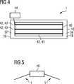
Auf dem Träger
Die erste Elektrode
Über der ersten Elektrode
Über der organischen funktionellen Schichtenstruktur
Die optoelektronische Schichtenstruktur ist ein elektrisch und/oder optisch aktiver Bereich. Der aktive Bereich ist beispielsweise der Bereich des organischen lichtemittierenden Bauelements
Über der zweiten Elektrode
In der Verkapselungsschicht
Über der Verkapselungsschicht
Über der Haftmittelschicht
Das organische lichtemittierende Bauelement
Die OLED
Außerhalb der Leuchtfläche
Die OLED
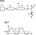
Die Antenne
Die Antenne
Die Antenne
Der Prozessor
Die Erfindung ist nicht auf die angegebenen Ausführungsbeispiele beschränkt. Beispielsweise können die Ausführungsbeispiele miteinander kombiniert werden. Beispielsweise können die in den
BezugszeichenlisteLIST OF REFERENCE NUMBERS
- 1 1
- organisches lichtemittierendes Bauelement organic light emitting device
- 12 12
- Träger carrier
- 14 14
- Metallschichtenstruktur Metal layer structure
- 16 16
- erster Kontaktabschnitt first contact section
- 18 18
- zweiter Kontaktabschnitt second contact section
- 20 20
- erste Elektrode first electrode
- 21 21
- Isolierungsbarriere isolation barrier
- 22 22
- organische funktionelle Schichtenstruktur organic functional layer structure
- 23 23
- zweite Elektrode second electrode
- 24 24
- Verkapselungsschicht encapsulation
- 32 32
- erster Kontaktbereich first contact area
- 34 34
- zweiter Kontaktbereich second contact area
- 36 36
- Haftmittelschicht Adhesive layer
- 38 38
- Abdeckkörper covering
- 40 40
- Leuchtfläche light area
- 42 42
- Antenne antenna
- 44 44
- elektronischer Schaltkreis electronic circuit
- 46 46
- Leuchte lamp
- 52 52
- Mikroprozessor microprocessor
- 54 54
- Modulator modulator
- 56 56
- Verstärker amplifier
- 58 58
- Kondensator capacitor
- 60 60
- Masseanschluss ground connection
- 70 70
- Signalmittelwert Signal averaging
- 7272
- moduliertes Signal modulated signal
- V_Bias VBIAS
- Gleichstrom direct current
Claims (14)
Translated fromGermanPriority Applications (2)
| Application Number | Priority Date | Filing Date | Title |
|---|---|---|---|
| DE102016105454.2ADE102016105454A1 (en) | 2016-03-23 | 2016-03-23 | Organic light-emitting device, method of manufacturing an organic light-emitting device, and method of operating an organic light-emitting device |
| PCT/EP2017/056630WO2017162631A1 (en) | 2016-03-23 | 2017-03-21 | Organic light-emitting component, method for producing an organic light-emitting component, and method for operating an organic light-emitting component |
Applications Claiming Priority (1)
| Application Number | Priority Date | Filing Date | Title |
|---|---|---|---|
| DE102016105454.2ADE102016105454A1 (en) | 2016-03-23 | 2016-03-23 | Organic light-emitting device, method of manufacturing an organic light-emitting device, and method of operating an organic light-emitting device |
Publications (1)
| Publication Number | Publication Date |
|---|---|
| DE102016105454A1true DE102016105454A1 (en) | 2017-09-28 |
Family
ID=58401550
Family Applications (1)
| Application Number | Title | Priority Date | Filing Date |
|---|---|---|---|
| DE102016105454.2APendingDE102016105454A1 (en) | 2016-03-23 | 2016-03-23 | Organic light-emitting device, method of manufacturing an organic light-emitting device, and method of operating an organic light-emitting device |
Country Status (2)
| Country | Link |
|---|---|
| DE (1) | DE102016105454A1 (en) |
| WO (1) | WO2017162631A1 (en) |
Citations (7)
| Publication number | Priority date | Publication date | Assignee | Title |
|---|---|---|---|---|
| DE102006033713A1 (en)* | 2006-05-30 | 2007-12-06 | Osram Opto Semiconductors Gmbh | Organic light-emitting component, device with an organic light-emitting component and illumination device, and method for producing an organic light-emitting component |
| DE102008035559A1 (en)* | 2008-07-30 | 2010-02-11 | Rupert Goihl | Light or voltage source has one or more luminophores in combination with electro-conductive particles, where light is generated from light source by electrically stimulated luminescence of luminophores |
| EP1519545B1 (en)* | 2003-09-29 | 2010-08-11 | LG Display Co., Ltd. | Folder type mobile terminal using organic electroluminescent panel and display method thereof |
| WO2011027280A1 (en)* | 2009-09-07 | 2011-03-10 | Koninklijke Philips Electronics N.V. | Wireless electroluminescent device |
| EP2728968A1 (en)* | 2012-01-05 | 2014-05-07 | Nitto Denko Corporation | Wireless power supply-type light-emitting element, and light-emitting device |
| DE102013207998A1 (en)* | 2013-05-02 | 2014-11-06 | Bundesdruckerei Gmbh | Security or value product with electroluminescent security element and method for producing the same |
| WO2015024633A1 (en)* | 2013-08-21 | 2015-02-26 | Diehl Ako Stiftung & Co. Kg | Lighting device and electronic domestic appliance having a lighting device of this type |
Family Cites Families (5)
| Publication number | Priority date | Publication date | Assignee | Title |
|---|---|---|---|---|
| JP2004164462A (en)* | 2002-11-15 | 2004-06-10 | Dainippon Printing Co Ltd | IC chip for contactless data carrier, contactless data carrier, and contactless data carrier utilization system |
| US20120105370A1 (en)* | 2005-12-12 | 2012-05-03 | Nupix, LLC | Electroded Sheet for a Multitude of Products |
| FR2940872B1 (en)* | 2009-01-07 | 2012-05-18 | Commissariat Energie Atomique | FLAT SCREEN WITH INTEGRATED ANTENNA |
| JP5209525B2 (en)* | 2009-02-05 | 2013-06-12 | トッパン・フォームズ株式会社 | card |
| JP5515540B2 (en)* | 2009-09-10 | 2014-06-11 | 富士通株式会社 | Display device |
- 2016
- 2016-03-23DEDE102016105454.2Apatent/DE102016105454A1/enactivePending
- 2017
- 2017-03-21WOPCT/EP2017/056630patent/WO2017162631A1/ennot_activeCeased
Patent Citations (7)
| Publication number | Priority date | Publication date | Assignee | Title |
|---|---|---|---|---|
| EP1519545B1 (en)* | 2003-09-29 | 2010-08-11 | LG Display Co., Ltd. | Folder type mobile terminal using organic electroluminescent panel and display method thereof |
| DE102006033713A1 (en)* | 2006-05-30 | 2007-12-06 | Osram Opto Semiconductors Gmbh | Organic light-emitting component, device with an organic light-emitting component and illumination device, and method for producing an organic light-emitting component |
| DE102008035559A1 (en)* | 2008-07-30 | 2010-02-11 | Rupert Goihl | Light or voltage source has one or more luminophores in combination with electro-conductive particles, where light is generated from light source by electrically stimulated luminescence of luminophores |
| WO2011027280A1 (en)* | 2009-09-07 | 2011-03-10 | Koninklijke Philips Electronics N.V. | Wireless electroluminescent device |
| EP2728968A1 (en)* | 2012-01-05 | 2014-05-07 | Nitto Denko Corporation | Wireless power supply-type light-emitting element, and light-emitting device |
| DE102013207998A1 (en)* | 2013-05-02 | 2014-11-06 | Bundesdruckerei Gmbh | Security or value product with electroluminescent security element and method for producing the same |
| WO2015024633A1 (en)* | 2013-08-21 | 2015-02-26 | Diehl Ako Stiftung & Co. Kg | Lighting device and electronic domestic appliance having a lighting device of this type |
Also Published As
| Publication number | Publication date |
|---|---|
| WO2017162631A1 (en) | 2017-09-28 |
Similar Documents
| Publication | Publication Date | Title |
|---|---|---|
| DE102014111345B4 (en) | Optoelectronic component and method for its production | |
| EP2323191A2 (en) | Organic photoelectric component | |
| WO2007036850A3 (en) | A large area organic diode device and a method of manufacturing it | |
| WO2014023807A2 (en) | Components and method for producing components | |
| US10804484B2 (en) | Lighting panel and method of fabricating the same, lighting module, lighting device, and lighting system | |
| DE112011104935T5 (en) | Organic electroluminescent device | |
| DE112011104929B4 (en) | Organic electroluminescent array | |
| US11825694B2 (en) | Array substrate comprising light shielding portion and method for manufacturing the same | |
| DE102010039956A1 (en) | Light source device and light source assembly | |
| US10418571B2 (en) | Lighting apparatus using organic light emitting device and method of fabricating thereof | |
| DE102014110052B4 (en) | Optoelectronic component and method for producing an optoelectronic component | |
| DE102014103747B4 (en) | Optoelectronic component and method for producing an optoelectronic component | |
| DE102014111346B4 (en) | Optoelectronic component device and method for producing an optoelectronic component device | |
| DE102013109814A1 (en) | Optoelectronic component, optoelectronic component device and method for producing an optoelectronic component | |
| US10892436B2 (en) | Narrow bezel electroluminance lighting device | |
| DE102016105454A1 (en) | Organic light-emitting device, method of manufacturing an organic light-emitting device, and method of operating an organic light-emitting device | |
| DE102013106688B4 (en) | Optoelectronic component and method for producing an optoelectronic component | |
| DE102010062021A1 (en) | Lighting device with organic light emitting diode | |
| DE102014218667B4 (en) | Optoelectronic assembly and method of manufacturing an optoelectronic assembly | |
| DE102015116055B4 (en) | Flat light-emitting component and method for producing a flat light-emitting component | |
| DE102013111736B4 (en) | Organic light-emitting diode and method for producing an organic light-emitting diode | |
| DE102013109898A1 (en) | Organic light-emitting component, method for producing an organic light-emitting component and illumination device for a motor vehicle | |
| EP2834862A1 (en) | Light-emission device with an oled element | |
| DE102013105228A1 (en) | Optoelectronic assembly, method of operating an optoelectronic assembly, and method of fabricating an optoelectronic assembly | |
| WO2016124587A1 (en) | Organic light-emitting component and light-emitting device |
Legal Events
| Date | Code | Title | Description |
|---|---|---|---|
| R163 | Identified publications notified | ||
| R082 | Change of representative | Representative=s name:EPPING HERMANN FISCHER PATENTANWALTSGESELLSCHA, DE | |
| R081 | Change of applicant/patentee | Owner name:PICTIVA DISPLAYS INTERNATIONAL LIMITED, IE Free format text:FORMER OWNER: OSRAM OLED GMBH, 93049 REGENSBURG, DE | |
| R082 | Change of representative | Representative=s name:EPPING HERMANN FISCHER PATENTANWALTSGESELLSCHA, DE | |
| R012 | Request for examination validly filed | ||
| R079 | Amendment of ipc main class | Free format text:PREVIOUS MAIN CLASS: H01L0051520000 Ipc:H10K0050800000 | |
| R016 | Response to examination communication |