DE102015208433A1 - RFID transponder with an integrated antenna arrangement - Google Patents
RFID transponder with an integrated antenna arrangementDownload PDFInfo
- Publication number
- DE102015208433A1 DE102015208433A1DE102015208433.7ADE102015208433ADE102015208433A1DE 102015208433 A1DE102015208433 A1DE 102015208433A1DE 102015208433 ADE102015208433 ADE 102015208433ADE 102015208433 A1DE102015208433 A1DE 102015208433A1
- Authority
- DE
- Germany
- Prior art keywords
- antenna
- rfid transponder
- dipole
- antenna arrangement
- transponder according
- Prior art date
- Legal status (The legal status is an assumption and is not a legal conclusion. Google has not performed a legal analysis and makes no representation as to the accuracy of the status listed.)
- Pending
Links
Images


Classifications
- G—PHYSICS
- G06—COMPUTING OR CALCULATING; COUNTING
- G06K—GRAPHICAL DATA READING; PRESENTATION OF DATA; RECORD CARRIERS; HANDLING RECORD CARRIERS
- G06K19/00—Record carriers for use with machines and with at least a part designed to carry digital markings
- G06K19/06—Record carriers for use with machines and with at least a part designed to carry digital markings characterised by the kind of the digital marking, e.g. shape, nature, code
- G06K19/067—Record carriers with conductive marks, printed circuits or semiconductor circuit elements, e.g. credit or identity cards also with resonating or responding marks without active components
- G06K19/07—Record carriers with conductive marks, printed circuits or semiconductor circuit elements, e.g. credit or identity cards also with resonating or responding marks without active components with integrated circuit chips
- G06K19/077—Constructional details, e.g. mounting of circuits in the carrier
- G06K19/07749—Constructional details, e.g. mounting of circuits in the carrier the record carrier being capable of non-contact communication, e.g. constructional details of the antenna of a non-contact smart card
- G06K19/07773—Antenna details
- G06K19/07786—Antenna details the antenna being of the HF type, such as a dipole
- G—PHYSICS
- G06—COMPUTING OR CALCULATING; COUNTING
- G06K—GRAPHICAL DATA READING; PRESENTATION OF DATA; RECORD CARRIERS; HANDLING RECORD CARRIERS
- G06K19/00—Record carriers for use with machines and with at least a part designed to carry digital markings
- G06K19/06—Record carriers for use with machines and with at least a part designed to carry digital markings characterised by the kind of the digital marking, e.g. shape, nature, code
- G06K19/067—Record carriers with conductive marks, printed circuits or semiconductor circuit elements, e.g. credit or identity cards also with resonating or responding marks without active components
- G06K19/07—Record carriers with conductive marks, printed circuits or semiconductor circuit elements, e.g. credit or identity cards also with resonating or responding marks without active components with integrated circuit chips
- G06K19/077—Constructional details, e.g. mounting of circuits in the carrier
- G06K19/07749—Constructional details, e.g. mounting of circuits in the carrier the record carrier being capable of non-contact communication, e.g. constructional details of the antenna of a non-contact smart card
- G06K19/07773—Antenna details
- G06K19/07794—Antenna details the record carrier comprising a booster or auxiliary antenna in addition to the antenna connected directly to the integrated circuit
- H—ELECTRICITY
- H01—ELECTRIC ELEMENTS
- H01Q—ANTENNAS, i.e. RADIO AERIALS
- H01Q1/00—Details of, or arrangements associated with, antennas
- H01Q1/12—Supports; Mounting means
- H01Q1/22—Supports; Mounting means by structural association with other equipment or articles
- H01Q1/2208—Supports; Mounting means by structural association with other equipment or articles associated with components used in interrogation type services, i.e. in systems for information exchange between an interrogator/reader and a tag/transponder, e.g. in Radio Frequency Identification [RFID] systems
- H01Q1/2225—Supports; Mounting means by structural association with other equipment or articles associated with components used in interrogation type services, i.e. in systems for information exchange between an interrogator/reader and a tag/transponder, e.g. in Radio Frequency Identification [RFID] systems used in active tags, i.e. provided with its own power source or in passive tags, i.e. deriving power from RF signal
- H—ELECTRICITY
- H01—ELECTRIC ELEMENTS
- H01Q—ANTENNAS, i.e. RADIO AERIALS
- H01Q9/00—Electrically-short antennas having dimensions not more than twice the operating wavelength and consisting of conductive active radiating elements
- H01Q9/04—Resonant antennas
- H01Q9/16—Resonant antennas with feed intermediate between the extremities of the antenna, e.g. centre-fed dipole
- H01Q9/20—Two collinear substantially straight active elements; Substantially straight single active elements
- H01Q9/24—Shunt feed arrangements to single active elements, e.g. for delta matching
- H—ELECTRICITY
- H04—ELECTRIC COMMUNICATION TECHNIQUE
- H04B—TRANSMISSION
- H04B5/00—Near-field transmission systems, e.g. inductive or capacitive transmission systems
- H04B5/40—Near-field transmission systems, e.g. inductive or capacitive transmission systems characterised by components specially adapted for near-field transmission
- H04B5/45—Transponders
- H—ELECTRICITY
- H04—ELECTRIC COMMUNICATION TECHNIQUE
- H04B—TRANSMISSION
- H04B5/00—Near-field transmission systems, e.g. inductive or capacitive transmission systems
- H04B5/70—Near-field transmission systems, e.g. inductive or capacitive transmission systems specially adapted for specific purposes
- H04B5/77—Near-field transmission systems, e.g. inductive or capacitive transmission systems specially adapted for specific purposes for interrogation
Landscapes
- Engineering & Computer Science (AREA)
- Computer Networks & Wireless Communication (AREA)
- Microelectronics & Electronic Packaging (AREA)
- Computer Hardware Design (AREA)
- Physics & Mathematics (AREA)
- General Physics & Mathematics (AREA)
- Theoretical Computer Science (AREA)
- Signal Processing (AREA)
- Variable-Direction Aerials And Aerial Arrays (AREA)
- Aerials With Secondary Devices (AREA)
- Details Of Aerials (AREA)
Abstract
Translated fromGermanDescription
Translated fromGermanZur Identifikation von Objekten werden heutzutage unteranderem UHF-RFID-Systeme eingesetzt, welche beispielsweise in [1] beschrieben sind. Ein solches System besteht aus einem stationären Gerät, dem RFID-Reader, und einem kleinen mobilen Gerät das an die zu identifizierenden Objekte angebracht ist, dem RIFD-Transponder. Dieser besteht üblicherweise aus einem RFID-Chip und einer separaten Antenne.Today, UHF RFID systems, which are described, for example, in [1], are used to identify objects. Such a system consists of a stationary device, the RFID reader, and a small mobile device attached to the objects to be identified, the RIFD transponder. This usually consists of an RFID chip and a separate antenna.
Aufgabe der vorliegenden Erfindung ist es, einen verbesserten RFID-Transponder bereitzustellen.The object of the present invention is to provide an improved RFID transponder.
Die Aufgabe wird gelöst durch einen RFID-Transponder umfassend einen Halbleiter-Chip mit einer auf einem Substrat ausgebildeten Passivierungsschicht, wobei eine Antennenanordnung zumindest teilweise in der Passivierungsschicht ausgebildet ist, wobei die Antennenanordnung einen Dipol zum Empfangen von Abfragesignalen und/oder zum Senden von Antwortsignalen, eine zu dem Dipol parallel geschaltete induktive Koppelschleife zum induktiven Ankoppeln einer außerhalb des Halbleiter-Chips ausgebildeten Booster Antenne, einen Reflektor zum Erhöhen eines Antennengewinns der Antennenanordnung sowie eine Anpassschaltung aufweist, wobei die Anpassschaltung zum Anpassen einer Impedanz der Antennenanordnung an eine Impedanz einer aktiven elektronischen Schaltung des RFID-Transponders zum Auswerten von den Abfragesignalen und/oder zum Erzeugen von den Antwortsignalen auf der Basis von den Abfragesignalen ausgebildet ist und wobei eine Speisung der Anpassschaltung elektrisch mit der aktiven elektronischen Schaltung zur Übertragung von den Abfragesignalen und/oder zur Übertragung von den Antwortsignalen verbunden ist.The object is achieved by an RFID transponder comprising a semiconductor chip with a passivation layer formed on a substrate, an antenna arrangement being formed at least partially in the passivation layer, the antenna arrangement having a dipole for receiving interrogation signals and / or for transmitting response signals, an inductive coupling loop connected in parallel with the dipole for inductively coupling a booster antenna formed outside the semiconductor chip, a reflector for increasing an antenna gain of the antenna arrangement and a matching circuit, the matching circuit for matching an impedance of the antenna arrangement to an impedance of an active electronic circuit the RFID transponder for evaluating the interrogation signals and / or for generating the response signals based on the interrogation signals is formed and wherein a supply of the matching circuit is electrically connected to the active electroni circuit for transmission of the interrogation signals and / or for transmission of the response signals is connected.
Die Erfindung schafft somit einen RFID-Transponder mit einer On-Chip Antenne, der beispielsweise mit einem Standard CMOS-Prozess hergestellt werden kann. Als On-Chip-Antennen werden Antennen bezeichnet die in den Halbleiter-Chip (auch Die genannt) integriert sind. Dadurch kann eine externe Antenne entfallen, so dass der RFID-Transponder im Wesentlichen aus einem einzigen Chip bestehen kann.The invention thus provides an RFID transponder with an on-chip antenna, which can be produced for example with a standard CMOS process. Antennas referred to as on-chip antennas are integrated in the semiconductor chip (also called die). As a result, an external antenna can be dispensed with, so that the RFID transponder can essentially consist of a single chip.
On-Chip-Antennen können prinzipiell verschieden ausgeführt sein, z. B. als Dipolantenne [
Es hat sich jedoch gezeigt, dass On-Chip Antennen, welche einen Dipol aufweisen, aufgrund der hohen Leitfähigkeit des Substrates (dotiertes Silizium) einen geringeren Antennengewinn als vergleichbare außerhalb des Chips angeordnete Antennen haben. Um diesen zu erhöhen können verschiedene Verfahren angewendet werden, so schlägt die Erfindung vor, die Abstrahlung in einen bestimmten Bereich zu bündeln. Erfindungsgemäß ist daher vorgesehen, dem Dipol einen Reflektor zur Fokussierung der Abstrahlung zuzuordnen. Über einen Reflektor kann die Abstrahlung der Antenne in eine Raumhälfte gebündelt werden, so dass sich ein höherer Antennengewinn ergibt. Der Reflektor kann länger oder kürzer als der Dipol sein.However, it has been found that on-chip antennas which have a dipole have a lower antenna gain than comparable off-chip antennas due to the high conductivity of the substrate (doped silicon). To increase this, various methods can be used, so the invention proposes to focus the radiation in a certain area. According to the invention, it is therefore provided to associate the dipole with a reflector for focusing the radiation. About a reflector, the radiation of the antenna can be bundled in a half of the room, so that there is a higher antenna gain. The reflector may be longer or shorter than the dipole.
Weiterhin ist eine Koppelschleife zur induktiven Ankopplung einer externen Booster Antenne vorgesehen, welche es ermöglicht, bei Bedarf durch induktive Kopplung externe Booster Antennen mit einem höheren Antennengewinn an den Chip anzukoppeln. Mittels der induktiven Kopplung können Booster Antennen ohne elektrische Verbindung mit der aktiven elektronischen Schaltung des RFID-Transponders (Sende- oder Empfangsschaltkreis) verbunden werden. Dabei können, je nach Einsatzbedingungen, verschiedene Antennenarten induktiv angekoppelt werden.Furthermore, a coupling loop for inductive coupling of an external booster antenna is provided, which makes it possible, if necessary, to couple external booster antennas with a higher antenna gain to the chip by inductive coupling. By means of inductive coupling booster antennas can be connected without electrical connection to the active electronic circuit of the RFID transponder (transmitting or receiving circuit). Depending on the operating conditions, different antenna types can be inductively coupled.
Weiterhin wird für eine gute Sende- bzw. Empfangsleistung des RFID-Transponders die Impedanz der Antenne mittels der Anpassschaltung an die Impedanz der aktiven elektronischen Schaltung angepasst. Die Anpassung kann über konzentrierte Bauelemente, insbesondere über passive konzentrierte Bauelemente, wie Induktivitäten und Kapazitäten, erfolgen, wobei verschiedene Anpassschaltungen möglich sind.Furthermore, for a good transmission or reception power of the RFID transponder, the impedance of the antenna is adapted by means of the matching circuit to the impedance of the active electronic circuit. The adaptation can take place via concentrated components, in particular via passive, concentrated components, such as inductors and capacitors, wherein different matching circuits are possible.
Die erfindungsgemäße Kombination der beschriebenen technischen Merkmale führt zu einem RFID-Transponder, bei dem das Verhältnis von Baugröße einerseits und Sende- bzw. Empfangsleistung andererseits optimiert ist.The inventive combination of technical features described leads to an RFID transponder, in which the ratio of size on the one hand and transmitting and receiving power on the other hand is optimized.
Gemäß einer bevorzugten Weiterbildung der Erfindung beträgt eine Arbeitsfrequenz des RFID-Transponders wenigstens 15 GHz, bevorzugt wenigstens 18 GHz, besonders bevorzugt wenigstens 21 GHz.According to a preferred embodiment of the invention, an operating frequency of the RFID transponder is at least 15 GHz, preferably at least 18 GHz, particularly preferably at least 21 GHz.
Bei herkömmlichen UHF RFID-Transpondern sind die Abmessungen des Halbleiter-Chips klein gegenüber der Antennenanordnung, sodass die Antenne für die Größe des Transponders ausschlaggebend ist. Deren Größe wiederrum hangt maßgeblich von der verwendeten Frequenz ab. Bei höheren Frequenzen wird die Antennenanordnung kleiner, sodass z. B. bei 24 GHz die Antennenanordnung eine Größe erreicht bei der sie direkt auf dem Halbleiter-Chip untergebracht werden kann (On-Chip Antenne). Damit ist ein RFID-Transponder möglich, der im Wesentlichen aus nur einem Chip besteht.With conventional UHF RFID transponders, the dimensions of the semiconductor chip are small compared to the antenna arrangement, so that the antenna is decisive for the size of the transponder is. Their size depends significantly on the frequency used. At higher frequencies, the antenna arrangement is smaller, so z. B. at 24 GHz, the antenna array reaches a size at which it can be accommodated directly on the semiconductor chip (on-chip antenna). Thus, an RFID transponder is possible, which essentially consists of only one chip.
Gemäß einer bevorzugten Weiterbildung der Erfindung ist eine Länge des Dipols kürzer als eine halbe Wellenlänge, welche in einem Vakuum einer Arbeitsfrequenz des RFID-Transponders entspricht. Hierdurch kann dem Umstand Rechnung getragen werden, dass bei einer gegebenen Arbeitsfrequenz die Wellenlänge im Dipol der Antennenanordnung aufgrund der hohen Permittivität des benachbarten Substrats geringer ist, als dies im Vakuum bzw. in der Atmosphäre der Fall ist.According to a preferred development of the invention, a length of the dipole is shorter than half a wavelength, which corresponds in a vacuum to an operating frequency of the RFID transponder. This can take into account the fact that at a given operating frequency, the wavelength in the dipole of the antenna array is lower due to the high permittivity of the adjacent substrate, as is the case in vacuum or in the atmosphere.
Gemäß einer bevorzugten Weiterbildung der Erfindung weist die Anpassschaltung eine T-Anpassstruktur, eine L-Anpassstruktur oder eine Pi-Anpassstruktur auf. Mit den genannten Anpassstrukturen kann auf einfache Weise Impedanz der Antennenanordnung an die Impedanz der aktiven elektronischen Schaltung des RFID-Transponders angepasst werden, so dass eine Leistungsanpassung erzielt ist.According to a preferred development of the invention, the matching circuit has a T-matching structure, an L-matching structure or a Pi-matching structure. With the said matching structures impedance of the antenna arrangement can be adapted to the impedance of the active electronic circuit of the RFID transponder in a simple manner, so that a power adjustment is achieved.
Gemäß einer vorteilhaften Weiterbildung der Erfindung ist die aktive elektronische Schaltung in den Halbleiter-Chip integriert. Auf diese Weise kann das Verhältnis von Baugröße einerseits und Sende- bzw. Empfangsleistung andererseits weiter optimiert werden.According to an advantageous development of the invention, the active electronic circuit is integrated in the semiconductor chip. In this way, the ratio of size on the one hand and transmitting and receiving power on the other hand can be further optimized.
Gemäß einer zweckmäßigen Weiterbildung der Erfindung weist die Passivierungsschicht wenigstens eine zum Substrat parallel verlaufende Metallschicht auf, wobei die Antennenanordnung in einer Metallschicht der wenigstens einen Metallschicht ausgebildet ist. Auf diese Weise kann eine besonders kompakte Antennenanordnung realisiert werden.According to an expedient development of the invention, the passivation layer has at least one metal layer extending parallel to the substrate, wherein the antenna arrangement is formed in a metal layer of the at least one metal layer. In this way, a particularly compact antenna arrangement can be realized.
Nach einer vorteilhaften Weiterbildung der Erfindung weist die Passivierungsschicht mehrere zum Substrat parallel verlaufende Metallschichten auf, wobei die Antennenanordnung in derjenigen Metallschicht der mehreren Metallschichten ausgebildet ist, welche den größten Abstand zum Substrat aufweist. Hierdurch kann die Sende- und Empfangsleistung weiter erhöht werden, da so der Einfluss des Substrats beim Senden bzw. Empfangen minimiert wird.According to an advantageous development of the invention, the passivation layer has a plurality of metal layers running parallel to the substrate, wherein the antenna arrangement is formed in that metal layer of the plurality of metal layers, which has the greatest distance from the substrate. As a result, the transmission and reception power can be increased further, since the influence of the substrate during transmission or reception is minimized.
Gemäß einer vorteilhaften Weiterbildung der Erfindung weist der Dipol auf beiden Seiten wenigstens einen Knick auf. Die beiden Knicke können insbesondere symmetrisch zu einer mittig angeordneten Speisung des Dipols angeordnet sein. Auf diese Weise kann eine kompakte Ausführung der Antennenanordnung realisiert werden.According to an advantageous development of the invention, the dipole has at least one kink on both sides. The two kinks may in particular be arranged symmetrically to a centrally arranged supply of the dipole. In this way, a compact design of the antenna arrangement can be realized.
Gemäß einer vorteilhaften Weiterbildung der Erfindung weist der Dipol auf beiden Seiten wenigstens eine Mäanderstruktur auf. Analog können auch hier die beiden Mäanderstrukturen symmetrisch zu einer mittig angeordneten Speisung des Dipols angeordnet sein. Es ergibt sich so eine besonders kompakte Ausführung der Antennenanordnung.According to an advantageous development of the invention, the dipole has at least one meandering structure on both sides. Analogously, the two meander structures can also be arranged symmetrically to a centrally arranged supply of the dipole. This results in a particularly compact design of the antenna arrangement.
Gemäß einer vorteilhaften Weiterbildung der Erfindung ist eine besagte Booster Antenne so angeordnet, dass sie mit der Koppelschleife induktiv gekoppelt ist. Hierdurch kann die Sende- und Empfangsleistung weiter erhöht werden.According to an advantageous embodiment of the invention, a said booster antenna is arranged so that it is inductively coupled to the coupling loop. As a result, the transmission and reception power can be further increased.
Nach einer zweckmäßigen Weiterbildung der Erfindung ist die Booster Antenne eine Panelantenne, welche auch Microstrip-Antenne genannt werden kann.According to an expedient development of the invention, the booster antenna is a panel antenna, which can also be called microstrip antenna.
Im Folgenden werden die vorliegende Erfindung und deren Vorteile anhand von Figuren näher beschrieben. Es zeigen:In the following, the present invention and its advantages will be described in more detail with reference to figures. Show it:
Gleiche oder gleichartige Elemente oder Elemente mit gleicher oder äquivalenter Funktion sind im Folgenden mit gleichen oder gleichartigen Bezugszeichen versehen.Identical or similar elements or elements with the same or equivalent function are provided below with the same or similar reference numerals.
In der folgenden Beschreibung werden Ausführungsbeispiele mit einer Vielzahl von Merkmalen der vorliegenden Erfindung näher beschrieben, um ein besseres Verständnis der Erfindung zu vermitteln. Es ist jedoch festzuhalten, dass die vorliegende Erfindung auch unter Auslassung einzelner der beschriebenen Merkmale umgesetzt werden kann. Es sei auch darauf hingewiesen, dass die in verschiedenen Ausführungsbeispielen gezeigten Merkmale auch in anderer Weise kombinierbar sind, sofern dies nicht ausdrücklich ausgeschlossen ist oder zu Widersprüchen führen würde.In the following description, embodiments having a plurality of features of the present invention will be described in detail to provide a better understanding of the invention. It should be noted, however, that the present invention also omits some of the described features can be implemented. It should also be noted that the features shown in various embodiments can also be combined in other ways, unless this is expressly excluded or would lead to contradictions.
Die Erfindung schafft somit einen RFID-Transponder mit einer On-Chip Antenne, der beispielsweise mit einem Standard CMOS-Prozess hergestellt werden kann. Als On-Chip-Antennen werden Antennen bezeichnet die in den Halbleiter-Chip (auch Die genannt) integriert sind. Dadurch kann eine externe Antenne entfallen, so dass der RFID-Transponder im Wesentlichen aus einem einzigen Chip bestehen kann.The invention thus provides an RFID transponder with an on-chip antenna, which can be produced for example with a standard CMOS process. Antennas referred to as on-chip antennas are integrated in the semiconductor chip (also called die). As a result, an external antenna can be dispensed with, so that the RFID transponder can essentially consist of a single chip.
On-Chip-Antennen können prinzipiell verschieden ausgeführt sein, z. B. als Dipolantenne [
Es hat sich jedoch gezeigt, dass On-Chip Antennen
Weiterhin ist eine Koppelschleife
Weiterhin wird für eine gute Sende- bzw. Empfangsleistung des RFID-Transponders
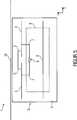
Die Antennenanordnung
Mit der Anpassschaltung
Die erfindungsgemäße Kombination der beschriebenen technischen Merkmale führt zu einem RFID-Transponder
Gemäß einer bevorzugten Weiterbildung der Erfindung beträgt eine Arbeitsfrequenz des RFID-Transponders
Bei herkömmlichen UHF RFID-Transpondern sind die Abmessungen des Halbleiter-Chips klein gegenüber der Antennenanordnung, sodass die Antenne für die Größe des Transponders ausschlaggebend ist. Deren Größe wiederrum hangt maßgeblich von der verwendeten Frequenz ab. Bei höheren Frequenzen wird die Antennenanordnung
Gemäß einer bevorzugten Weiterbildung der Erfindung ist eine Länge des Dipols
Gemäß einer bevorzugten Weiterbildung der Erfindung weist die Anpassschaltung
Gemäß einer vorteilhaften Weiterbildung der Erfindung ist die aktive elektronische Schaltung
Gemäß einer zweckmäßigen Weiterbildung der Erfindung weist die Passivierungsschicht
Nach einer vorteilhaften Weiterbildung der Erfindung weist die Passivierungsschicht
Gemäß einer vorteilhaften Weiterbildung der Erfindung weist der Dipol
Gemäß einer vorteilhaften Weiterbildung der Erfindung weist der Dipol
Gemäß einer vorteilhaften Weiterbildung der Erfindung ist eine besagte Booster Antenne
Nach einer zweckmäßigen Weiterbildung der Erfindung ist die Booster Antenne
BezugszeichenlisteLIST OF REFERENCE NUMBERS
- 11
- RFID-TransponderRFID transponder
- 22
- Halbleiter-ChipSemiconductor chip
- 33
- Passivierungsschichtpassivation
- 44
- Dipoldipole
- 55
- induktive Koppelschleifeinductive coupling loop
- 66
- Reflektorreflector
- 77
- Anpassschaltungmatching
- 88th
- aktive elektronische Schaltungactive electronic circuit
- 99
- Speisungsupply
- 1010
- Substratsubstratum
- 1111
- Metallschichtmetal layer
- 1212
- Metallschichtmetal layer
- 1313
- Metallschichtmetal layer
- 1414
- Knickkink
- 1515
- Mäanderstrukturmeandering
- 1616
- Booster AntenneBooster antenna
Quellen:Sources:
- [1]
K. Finkenzeller, RFID-Handbuch. 5., aktualisierte und erw. Aufl., Hanser 2008 K. Finkenzeller, RFID manual. 5th, updated and upgraded Edition, Hanser 2008 - [2]
F. Toutai, M. Ponts, On-Chip integration of dipole antenna and VCO using standard BiCMOS technology for 10 GHz applications, Proceedings of the 29th European Solid-State Circuits Conference, 2003 F. Toutai, M. Ponts, on-chip integration of dipole antenna and VCO using standard BiCMOS technology for 10 GHz applications, Proceedings of the 29th European Solid-State Circuits Conference, 2003 - [3]
Y. P. Zhang, M. Sun, L. H. Guo, On-Chip Antennas for 60-GHz Radios in Silicon Technology, IEEE Transactions on Electron Devices, vol. 52, n. 7, pp. 1664–1668, July 2005 YP Zhang, M. Sun, LH Guo, On-Chip Antennas for 60GHz Radios in Silicon Technology, IEEE Transactions on Electron Devices, vol. 52, n. 7, pp. 1664-1668, July 2005 - [4]
K.- K. Huang, D. D. Wentzloff, 60 GHz On-Chip Patch Antenna Integrated in a 0. 13-μm CMOS Technology, IEEE International Conference on Ultra-Wideband 2010 K.-K. Huang, DD Wentzloff, 60GHz On-Chip Patch Antenna Integrated in a 0. 13-μm CMOS Technology, IEEE International Conference on Ultra Wideband 2010 - [5]
D. Dancila, R. Malmqvist, R. Augustine, C. Samuelsson, M. Kaynak, A. Rydberg, Wide Band On-Chip Slot Antenna with Back-Side Etched Trench for W-band Sensing Applications, 7th European Conference on Antennas and Propagation (EuCAP), 2013 D. Dancila, R. Malmqvist, R. Augustine, C. Samuelsson, M. Kaynak, A. Rydberg, Wide Band On-Chip Slot Antenna with Back-Side Etched Trench for W-band Sensing Applications, 7th European Conference on Antennas and Propagation (EuCAP), 2013 - [6]
H. Choo, H. Ling, Design of electrically small planar antennas using inductively coupled feed, Electronics Letters, vol 39, n. 22, pp. 1563–1565, Oct. 2003 H. Choo, H. Ling, Design of Electrically Small Planar Antennas Using inductively-coupled feed, Electronics Letters, vol 39, n. 22, pp. 1563-1565, Oct. 2003 - [7]
Sun Xu-Bao, Xie Jun, Cao Mao-Young, RFID Tag Antenna Design Based on an Improved Coupling Source Shape, IEEE Antennas and Wireless Propagation Letters, vol. 12, pp. 532–534 Sun Xu-Bao, Xie Jun, Cao Mao-Young, RFID Tag Antenna Design Based on Improved Coupling Source Shape, IEEE Antennas and Wireless Propagation Letters, vol. 12, pp. 532-534 - [8]
K. Jeong-Seok, C. Wonkyu, C. Jong-Suk, Ceramic Patch Antenna using inductive coupled feed for UHF RFID Tag Mountable On Metallic Objects, Asia-Pacific Microwave Conference 2008 K. Jeong-Seok, C. Wonkyu, C. Jong-Suk, Ceramic Patch Antenna using UFO RFID Tag Mountable On Metallic Objects, Asia-Pacific Microwave Conference 2008 - [9]
F. Alimenti, M. Virili, P. Mezzanotte, V. Palazzari, M. M. Tentzeris, L. Roselli, Low-Cost Assembly of UHF RFID Chips and Flexible Substrate Antennas by Magnetic Coupling Approach, IEEE International Microwave Symposium Digest (MTI), 2010 F. Alimenti, M. Virili, P. Mezzanotte, V. Palazzari, MM Tentzeris, L. Roselli, Low-Cost Assembly of UHF RFID Chips and Flexible Substrates Antennas by Magnetic Coupling Approach, IEEE International Microwave Symposium Digest (MTI), 2010 - [10]
G. Marrocco, The Art of UHF RFID Antenna Design: Impedance-Matching and Size-Reduction Techniques, IEEE Antennas and Propagation Magazine, vol. 50, n. 1, pp. 66–79, Feb. 2008 G. Marrocco, The Art of UHF RFID Antenna Design: Impedance Matching and Size-Reduction Techniques, IEEE Antennas and Propagation Magazine, vol. 50, n. 1, pp. 66-79, Feb. 2008
Claims (11)
Translated fromGermanPriority Applications (1)
| Application Number | Priority Date | Filing Date | Title |
|---|---|---|---|
| DE102015208433.7ADE102015208433A1 (en) | 2015-05-06 | 2015-05-06 | RFID transponder with an integrated antenna arrangement |
Applications Claiming Priority (1)
| Application Number | Priority Date | Filing Date | Title |
|---|---|---|---|
| DE102015208433.7ADE102015208433A1 (en) | 2015-05-06 | 2015-05-06 | RFID transponder with an integrated antenna arrangement |
Publications (1)
| Publication Number | Publication Date |
|---|---|
| DE102015208433A1true DE102015208433A1 (en) | 2016-11-10 |
Family
ID=57178786
Family Applications (1)
| Application Number | Title | Priority Date | Filing Date |
|---|---|---|---|
| DE102015208433.7APendingDE102015208433A1 (en) | 2015-05-06 | 2015-05-06 | RFID transponder with an integrated antenna arrangement |
Country Status (1)
| Country | Link |
|---|---|
| DE (1) | DE102015208433A1 (en) |
Cited By (1)
| Publication number | Priority date | Publication date | Assignee | Title |
|---|---|---|---|---|
| CN115939728A (en)* | 2022-10-24 | 2023-04-07 | 华南理工大学 | Millimeter wave dual-frequency on-chip antenna with gain enhanced through packaging technology |
Citations (8)
| Publication number | Priority date | Publication date | Assignee | Title |
|---|---|---|---|---|
| US20050151698A1 (en)* | 2002-11-19 | 2005-07-14 | Farrokh Mohamadi | Beam forming antenna array on transparent substrate |
| US7126554B2 (en)* | 2002-11-19 | 2006-10-24 | Farrokh Mohamadi | Integrated circuit waveguide |
| DE102005042444A1 (en)* | 2005-09-06 | 2007-03-22 | Ksw Microtec Ag | Arrangement for an RFID transponder antenna |
| WO2008129125A1 (en)* | 2007-04-19 | 2008-10-30 | Pulse Finland Oy | Method and arrangement for matching an antenna |
| US20100134292A1 (en)* | 2008-12-03 | 2010-06-03 | Deavours Daniel D | Radio-frequency identification device with foam substrate |
| US20100283694A1 (en)* | 2008-03-03 | 2010-11-11 | Murata Manufacturing Co., Ltd. | Composite antenna |
| US20120280873A1 (en)* | 2006-12-29 | 2012-11-08 | Broadcom Corporation | Integrated circuit mems antenna structure |
| US20130126622A1 (en)* | 2011-08-08 | 2013-05-23 | David Finn | Offsetting shielding and enhancing coupling in metallized smart cards |
- 2015
- 2015-05-06DEDE102015208433.7Apatent/DE102015208433A1/enactivePending
Patent Citations (8)
| Publication number | Priority date | Publication date | Assignee | Title |
|---|---|---|---|---|
| US20050151698A1 (en)* | 2002-11-19 | 2005-07-14 | Farrokh Mohamadi | Beam forming antenna array on transparent substrate |
| US7126554B2 (en)* | 2002-11-19 | 2006-10-24 | Farrokh Mohamadi | Integrated circuit waveguide |
| DE102005042444A1 (en)* | 2005-09-06 | 2007-03-22 | Ksw Microtec Ag | Arrangement for an RFID transponder antenna |
| US20120280873A1 (en)* | 2006-12-29 | 2012-11-08 | Broadcom Corporation | Integrated circuit mems antenna structure |
| WO2008129125A1 (en)* | 2007-04-19 | 2008-10-30 | Pulse Finland Oy | Method and arrangement for matching an antenna |
| US20100283694A1 (en)* | 2008-03-03 | 2010-11-11 | Murata Manufacturing Co., Ltd. | Composite antenna |
| US20100134292A1 (en)* | 2008-12-03 | 2010-06-03 | Deavours Daniel D | Radio-frequency identification device with foam substrate |
| US20130126622A1 (en)* | 2011-08-08 | 2013-05-23 | David Finn | Offsetting shielding and enhancing coupling in metallized smart cards |
Non-Patent Citations (9)
| Title |
|---|
| D. Dancila, R. Malmqvist, R. Augustine, C. Samuelsson, M. Kaynak, A. Rydberg, Wide Band On-Chip Slot Antenna with Back-Side Etched Trench for W-band Sensing Applications, 7th European Conference on Antennas and Propagation (EuCAP), 2013 |
| F. Alimenti, M. Virili, P. Mezzanotte, V. Palazzari, M. M. Tentzeris, L. Roselli, Low-Cost Assembly of UHF RFID Chips and Flexible Substrate Antennas by Magnetic Coupling Approach, IEEE International Microwave Symposium Digest (MTI), 2010 |
| F. Toutai, M. Ponts, On-Chip integration of dipole antenna and VCO using standard BiCMOS technology for 10 GHz applications, Proceedings of the 29th European Solid-State Circuits Conference, 2003 |
| G. Marrocco, The Art of UHF RFID Antenna Design: Impedance-Matching and Size-Reduction Techniques, IEEE Antennas and Propagation Magazine, vol. 50, n. 1, pp. 66–79, Feb. 2008 |
| H. Choo, H. Ling, Design of electrically small planar antennas using inductively coupled feed, Electronics Letters, vol 39, n. 22, pp. 1563–1565, Oct. 2003 |
| K. Jeong-Seok, C. Wonkyu, C. Jong-Suk, Ceramic Patch Antenna using inductive coupled feed for UHF RFID Tag Mountable On Metallic Objects, Asia-Pacific Microwave Conference 2008 |
| K.- K. Huang, D. D. Wentzloff, 60 GHz On-Chip Patch Antenna Integrated in a 0. 13-μm CMOS Technology, IEEE International Conference on Ultra-Wideband 2010 |
| Sun Xu-Bao, Xie Jun, Cao Mao-Young, RFID Tag Antenna Design Based on an Improved Coupling Source Shape, IEEE Antennas and Wireless Propagation Letters, vol. 12, pp. 532–534 |
| Y. P. Zhang, M. Sun, L. H. Guo, On-Chip Antennas for 60-GHz Radios in Silicon Technology, IEEE Transactions on Electron Devices, vol. 52, n. 7, pp. 1664–1668, July 2005 |
Cited By (1)
| Publication number | Priority date | Publication date | Assignee | Title |
|---|---|---|---|---|
| CN115939728A (en)* | 2022-10-24 | 2023-04-07 | 华南理工大学 | Millimeter wave dual-frequency on-chip antenna with gain enhanced through packaging technology |
Similar Documents
| Publication | Publication Date | Title |
|---|---|---|
| DE112008000065B4 (en) | Wireless IC device | |
| DE102010001407B4 (en) | Integrated wafer-level antennas | |
| DE112016007571T5 (en) | MICROELECTRONIC COMPONENTS DESIGNED WITH FLEXIBLE HOUSING SUBSTRATES WITH DISTRIBUTED STACKED ANTENNAS FOR HIGH FREQUENCY COMMUNICATION SYSTEMS | |
| DE112017001710T5 (en) | Microwave antenna device, packaging and manufacturing process | |
| DE112015005575T5 (en) | MICROWAVE ANTENNA DEVICE, UNIT AND MANUFACTURING METHOD | |
| DE102013218742A1 (en) | Antenna for vehicle | |
| EP2820674B1 (en) | Semiconductor module having integrated antenna structures | |
| DE102008063198A1 (en) | antenna device | |
| DE102013003179A1 (en) | Multi-antenna isolation | |
| DE102019118691A1 (en) | SEMICONDUCTOR HOUSING WITH PLASTIC WAVE GUIDE | |
| DE102021102228A1 (en) | Radio frequency devices and method of manufacturing radio frequency devices | |
| DE102020112787A1 (en) | High frequency device with high frequency chip and waveguide structure | |
| DE112009002384T5 (en) | Antenna and wireless ic component | |
| DE212018000050U1 (en) | Ultra-wideband antenna | |
| DE102017112894A1 (en) | High-frequency component, in particular for radar applications | |
| US10615494B2 (en) | Coupling reduction method for antennas in package | |
| DE102015207186A1 (en) | Antenna device for implementing orthogonal antenna characteristics | |
| DE102014218339A1 (en) | Device for transmitting millimeter-wave signals | |
| DE102020121855A1 (en) | Radio frequency devices and associated manufacturing processes | |
| DE102004045707A1 (en) | antenna | |
| DE102013201222A1 (en) | antenna device | |
| EP3503290B1 (en) | Antenna device with bond wires | |
| DE102019128779B4 (en) | High frequency device with high frequency signal routing element and associated manufacturing process | |
| DE102015208433A1 (en) | RFID transponder with an integrated antenna arrangement | |
| EP2939308B1 (en) | Chip antenna, electronic component, and method for producing same |
Legal Events
| Date | Code | Title | Description |
|---|---|---|---|
| R012 | Request for examination validly filed | ||
| R016 | Response to examination communication |