DE102014112681A1 - Optoelectronic semiconductor device and flashlight - Google Patents
Optoelectronic semiconductor device and flashlightDownload PDFInfo
- Publication number
- DE102014112681A1 DE102014112681A1DE102014112681.5ADE102014112681ADE102014112681A1DE 102014112681 A1DE102014112681 A1DE 102014112681A1DE 102014112681 ADE102014112681 ADE 102014112681ADE 102014112681 A1DE102014112681 A1DE 102014112681A1
- Authority
- DE
- Germany
- Prior art keywords
- color
- cie
- loci
- planck curve
- coordinate
- Prior art date
- Legal status (The legal status is an assumption and is not a legal conclusion. Google has not performed a legal analysis and makes no representation as to the accuracy of the status listed.)
- Withdrawn
Links
Images


Classifications
- H—ELECTRICITY
- H01—ELECTRIC ELEMENTS
- H01L—SEMICONDUCTOR DEVICES NOT COVERED BY CLASS H10
- H01L25/00—Assemblies consisting of a plurality of semiconductor or other solid state devices
- H01L25/03—Assemblies consisting of a plurality of semiconductor or other solid state devices all the devices being of a type provided for in a single subclass of subclasses H10B, H10D, H10F, H10H, H10K or H10N, e.g. assemblies of rectifier diodes
- H01L25/04—Assemblies consisting of a plurality of semiconductor or other solid state devices all the devices being of a type provided for in a single subclass of subclasses H10B, H10D, H10F, H10H, H10K or H10N, e.g. assemblies of rectifier diodes the devices not having separate containers
- H01L25/075—Assemblies consisting of a plurality of semiconductor or other solid state devices all the devices being of a type provided for in a single subclass of subclasses H10B, H10D, H10F, H10H, H10K or H10N, e.g. assemblies of rectifier diodes the devices not having separate containers the devices being of a type provided for in group H10H20/00
- H01L25/0753—Assemblies consisting of a plurality of semiconductor or other solid state devices all the devices being of a type provided for in a single subclass of subclasses H10B, H10D, H10F, H10H, H10K or H10N, e.g. assemblies of rectifier diodes the devices not having separate containers the devices being of a type provided for in group H10H20/00 the devices being arranged next to each other
- H—ELECTRICITY
- H10—SEMICONDUCTOR DEVICES; ELECTRIC SOLID-STATE DEVICES NOT OTHERWISE PROVIDED FOR
- H10H—INORGANIC LIGHT-EMITTING SEMICONDUCTOR DEVICES HAVING POTENTIAL BARRIERS
- H10H20/00—Individual inorganic light-emitting semiconductor devices having potential barriers, e.g. light-emitting diodes [LED]
- H10H20/80—Constructional details
- H10H20/85—Packages
- H10H20/851—Wavelength conversion means
- H10H20/8515—Wavelength conversion means not being in contact with the bodies
- H—ELECTRICITY
- H01—ELECTRIC ELEMENTS
- H01L—SEMICONDUCTOR DEVICES NOT COVERED BY CLASS H10
- H01L2924/00—Indexing scheme for arrangements or methods for connecting or disconnecting semiconductor or solid-state bodies as covered by H01L24/00
- H01L2924/0001—Technical content checked by a classifier
- H01L2924/0002—Not covered by any one of groups H01L24/00, H01L24/00 and H01L2224/00
- H—ELECTRICITY
- H04—ELECTRIC COMMUNICATION TECHNIQUE
- H04M—TELEPHONIC COMMUNICATION
- H04M1/00—Substation equipment, e.g. for use by subscribers
- H04M1/02—Constructional features of telephone sets
- H04M1/21—Combinations with auxiliary equipment, e.g. with clocks or memoranda pads
- H—ELECTRICITY
- H05—ELECTRIC TECHNIQUES NOT OTHERWISE PROVIDED FOR
- H05B—ELECTRIC HEATING; ELECTRIC LIGHT SOURCES NOT OTHERWISE PROVIDED FOR; CIRCUIT ARRANGEMENTS FOR ELECTRIC LIGHT SOURCES, IN GENERAL
- H05B45/00—Circuit arrangements for operating light-emitting diodes [LED]
- H05B45/20—Controlling the colour of the light
- H—ELECTRICITY
- H05—ELECTRIC TECHNIQUES NOT OTHERWISE PROVIDED FOR
- H05B—ELECTRIC HEATING; ELECTRIC LIGHT SOURCES NOT OTHERWISE PROVIDED FOR; CIRCUIT ARRANGEMENTS FOR ELECTRIC LIGHT SOURCES, IN GENERAL
- H05B47/00—Circuit arrangements for operating light sources in general, i.e. where the type of light source is not relevant
- H05B47/10—Controlling the light source
- H05B47/105—Controlling the light source in response to determined parameters
- H05B47/11—Controlling the light source in response to determined parameters by determining the brightness or colour temperature of ambient light
- H—ELECTRICITY
- H10—SEMICONDUCTOR DEVICES; ELECTRIC SOLID-STATE DEVICES NOT OTHERWISE PROVIDED FOR
- H10H—INORGANIC LIGHT-EMITTING SEMICONDUCTOR DEVICES HAVING POTENTIAL BARRIERS
- H10H20/00—Individual inorganic light-emitting semiconductor devices having potential barriers, e.g. light-emitting diodes [LED]
- H10H20/80—Constructional details
- H10H20/85—Packages
- H10H20/851—Wavelength conversion means
- H10H20/8511—Wavelength conversion means characterised by their material, e.g. binder
- H10H20/8512—Wavelength conversion materials
- H10H20/8513—Wavelength conversion materials having two or more wavelength conversion materials
- H—ELECTRICITY
- H10—SEMICONDUCTOR DEVICES; ELECTRIC SOLID-STATE DEVICES NOT OTHERWISE PROVIDED FOR
- H10H—INORGANIC LIGHT-EMITTING SEMICONDUCTOR DEVICES HAVING POTENTIAL BARRIERS
- H10H20/00—Individual inorganic light-emitting semiconductor devices having potential barriers, e.g. light-emitting diodes [LED]
- H10H20/80—Constructional details
- H10H20/85—Packages
- H10H20/851—Wavelength conversion means
- H10H20/8516—Wavelength conversion means having a non-uniform spatial arrangement or non-uniform concentration, e.g. patterned wavelength conversion layer or wavelength conversion layer with a concentration gradient
Landscapes
- Engineering & Computer Science (AREA)
- Power Engineering (AREA)
- Microelectronics & Electronic Packaging (AREA)
- Physics & Mathematics (AREA)
- Condensed Matter Physics & Semiconductors (AREA)
- General Physics & Mathematics (AREA)
- Computer Hardware Design (AREA)
- Led Device Packages (AREA)
Abstract
Translated fromGermanDescription
Translated fromGermanEs wird ein optoelektronisches Halbleiterbauteil angegeben. Darüber hinaus wird ein Blitzlicht mit einem solchen Halbleiterbauteil angegeben.An optoelectronic semiconductor component is specified. In addition, a flash is specified with such a semiconductor device.
Eine zu lösende Aufgabe besteht darin, ein optoelektronisches Halbleiterbauteil, insbesondere für Blitzlichtanwendungen, anzugeben, dessen Emissionsspektrum flexibel einstellbar ist.An object to be solved is to specify an optoelectronic semiconductor component, in particular for flash applications, whose emission spectrum is flexibly adjustable.
Diese Aufgabe wird unter anderem durch ein optoelektronisches Halbleiterbauteil und durch ein Blitzlicht mit den Merkmalen der unabhängigen Patentansprüche gelöst. Bevorzugte Weiterbildungen sind Gegenstand der abhängigen Ansprüche.This object is achieved inter alia by an optoelectronic semiconductor device and by a flash with the features of the independent claims. Preferred developments are the subject of the dependent claims.
Gemäß zumindest einer Ausführungsform umfasst das optoelektronische Halbleiterbauteil mindestens eine erste Lichtquelle, mindestens eine zweite Lichtquelle, mindestens eine dritte Lichtquelle und mindestens eine vierte Lichtquelle. Die Lichtquellen sind hinsichtlich ihres Emissionsspektrums verschieden voneinander. Mit anderen Worten umfasst das optoelektronische Halbleiterbauteil vier oder mehr als vier voneinander verschiedene Lichtquellen. Jede Lichtquelle weist ein bestimmtes Emissionsspektrum auf.In accordance with at least one embodiment, the optoelectronic semiconductor component comprises at least one first light source, at least one second light source, at least one third light source, and at least one fourth light source. The light sources are different from each other in terms of their emission spectrum. In other words, the optoelectronic semiconductor device comprises four or more than four different light sources. Each light source has a specific emission spectrum.
Gemäß zumindest einer Ausführungsform weist jede der Lichtquellen des Halbleiterbauteils einen oder mehrere optoelektronische Halbleiterchips auf. Beispielsweise handelt es sich bei den Halbleiterchips um Leuchtdiodenchips oder Laserdiodenchips.In accordance with at least one embodiment, each of the light sources of the semiconductor component has one or more optoelectronic semiconductor chips. By way of example, the semiconductor chips are light-emitting diode chips or laser diode chips.
Gemäß zumindest einer Ausführungsform emittieren die mindestens vier verschiedenen Lichtquellen im Betrieb jeweils Strahlung mit voneinander verschiedenen Farborten. Bei den Farborten handelt es sich um Farborte in der CIE-Normfarbtafel. Die Darstellung kann beispielsweise in einem CIE-xy-Diagramm, in einem CIE-uv-Diagramm oder in einem CIE-u’v’-Diagramm erfolgen. Die einzelnen, verschiedenen CIE-Darstellungen sind ineinander umrechenbar, beispielsweise wie der Druckschrift
Gemäß zumindest einer Ausführungsform liegen zumindest zwei der Farborte der im Betrieb von den Lichtquellen emittierten Strahlungsspektren in der CIE-Normfarbtafel auf einer gemeinsamen Isothermen. Ebenso ist es möglich, dass diese Farborte auf einer gemeinsamen Verlängerungsgeraden, die eine Isotherme verlängert, liegen. Isothermen sind dabei Linien, die im CIE-uv-Diagramm senkrecht zur Schwarzkörperkurve, auch als Planck-Kurve bezeichnet, liegen, siehe auch zum Beispiel die Druckschrift
Gemäß zumindest einer Ausführungsform liegen zumindest zwei Farborte mit einer Toleranz von höchstens einer Drei-Schritte-MacAdam-Ellipse auf der gemeinsamen Isothermen oder der gemeinsamen Verlängerungsgeraden. Eine Ein-Schritt-MacAdam-Ellipse ist dabei ein Bereich, innerhalb dessen ein Standardbetrachter in der CIE-Normfarbtafel keinen Farbunterschied feststellen kann. Das Konzept der MacAdam-Ellipsen ist beispielsweise erläutert in der Druckschrift
Gemäß zumindest einer Ausführungsform ist das Halbleiterbauteil dazu eingerichtet, im Betrieb farbiges Licht oder weißes Licht mit einer veränderbaren korrelierten Farbtemperatur, auch als correlated color temperature oder kurz CCT bezeichnet, zu emittieren. Weißes Licht bedeutet insbesondere, dass ein Farbort der insgesamt von dem Halbleiterbauteil emittierten Strahlung dann einen Abstand von höchstens 0,05 Einheiten oder 0,03 Einheiten oder 0,01 Einheiten oder von höchstens einer Fünf-Schritte-MacAdam-Ellipse oder höchstens einer Drei-Schritte-MacAdam-Ellipse von der Planck-Kurve in der CIE-uv-Darstellung aufweist. Mit anderen Worten strahlt das Halbleiterbauteil im bestimmungsgemäßen Gebrauch Licht ab, das einem Betrachter weiß erscheint. Die von dem Halbleiterbauteil emittierte Mischstrahlung ist gezielt und reproduzierbar einstellbar.In accordance with at least one embodiment, the semiconductor device is configured to emit in operation colored light or white light having a changeable correlated color temperature, also referred to as correlated color temperature or CCT for short. In particular, white light means that a color location of the total radiation emitted by the semiconductor component is a distance of at most 0.05 units or 0.03 units or 0.01 units or of at most one five-step MacAdam ellipse or at most one third. Steps MacAdam ellipse from the Planck curve in the CIE uv representation. In other words, when used as intended, the semiconductor device emits light that appears white to a viewer. The mixed radiation emitted by the semiconductor component can be adjusted in a targeted and reproducible manner.
In mindestens einer Ausführungsform umfasst das optoelektronische Halbleiterbauteil mindestens vier verschiedene Lichtquellen mit je mindestens einem optoelektronischen Halbleiterchip. Im Betrieb emittieren die Lichtquellen eine Strahlung mit voneinander verschiedenen Farborten in der CIE-Normfarbtafel. Bevorzugt liegen zumindest zwei der Farborte in der CIE-Normfarbtafel auf einer gemeinsamen Isothermen oder auf einer gemeinsamen Verlängerungsgeraden, die eine Isotherme verlängert. Die Farborte liegen dann mit einer Toleranz von höchstens einer Drei-Schritte-MacAdam-Ellipse auf der Isothermen oder der Verlängerungsgeraden. Das Halbleiterbauteil ist außerdem bevorzugt dazu eingerichtet, im Betrieb weißes Licht zu emittieren, wobei eine Farbtemperatur des weißen Lichts veränderbar und durchstimmbar ist.In at least one embodiment, the optoelectronic semiconductor component comprises at least four different light sources each having at least one optoelectronic semiconductor chip. In operation, the light sources emit radiation with mutually different color locations in the CIE standard color chart. Preferably, at least two of the color loci in the CIE standard color chart are on a common isotherm or on a common extension line extending an isotherm. The color locations will then lie with a tolerance of at most a three-step MacAdam ellipse on the isotherms or the extension line. The semiconductor device is also preferred configured to emit white light in operation, wherein a color temperature of the white light is changeable and tunable.
Bei Blitzlichtanwendungen, etwa in Mobiltelefonen und tragbaren Kameras, mischt sich häufig bei der Fotografie das eigentliche Blitzlicht mit Umgebungslicht. Da es eine Vielzahl von unterschiedlichen Umgebungslichtarten gibt, wie unterschiedliche Tageszeiten oder unterschiedliche künstliche Beleuchtungen etwa durch Fluoreszenzlampen oder Energiesparlampen, führt es zu einer erheblichen Verbesserung eines Weißabgleichs und einer Bildqualität, wenn das Licht des Blitzlichts auf das Umgebungslicht angepasst wird. Typischerweise kann dies nicht durch eine einzelne Lichtquelle oder durch eine einzelne Leuchtdiode, kurz LED, erreicht werden, sondern muss in der Regel durch zwei oder mehrere Lichtquellen oder LEDs samt zugehörigen Leuchtstoffen erreicht werden.In flash applications, such as in mobile phones and portable cameras, the actual flash often mixes with ambient light in photography. Since there are a variety of different types of ambient light, such as different times of day or different artificial lighting such as fluorescent or energy-saving lamps, it leads to a significant improvement in white balance and image quality when the light of the flash is adapted to the ambient light. Typically, this can not be achieved by a single light source or by a single light emitting diode, in short LED, but must typically be achieved by two or more light sources or LEDs and associated phosphors.
Eine Möglichkeit, unterschiedliches Licht abstrahlende Lichtquellen zu realisieren, besteht darin, den Lichtweg mehrerer Halbleiterchips in dem Halbleiterbauteil durch unterschiedliche Leuchtstoffe und/oder unterschiedliche Leuchtstoffmengen zu führen. Durch die Mischung des Lichts der einzelnen Lichtquellen in unterschiedlichen Verhältnissen kann eine Vielzahl von unterschiedlichen Farborten der insgesamt emittierten Strahlung mit dem Halbleiterbauteil erreicht werden, ohne dass zusätzliche Lichtquellen erforderlich sind. Dies führt zu einer erheblichen Verbesserung der Bildqualität.One way to realize different light emitting light sources, is to guide the light path of multiple semiconductor chips in the semiconductor device by different phosphors and / or different amounts of phosphor. By mixing the light of the individual light sources in different ratios, a multiplicity of different color locations of the total emitted radiation with the semiconductor component can be achieved without the need for additional light sources. This leads to a significant improvement in image quality.
Insbesondere gegenüber von LED-Bauteilen mit nur zwei oder drei Halbleiterchips mit zugeordnetem Leuchtstoff und/oder mit unterschiedlichen Emissionswellenlängen sind eine Effizienz und/oder eine Farbwiedergabequalität verbesserbar. So ist eine Reabsorption von bereits konvertierter Strahlung in einem Leuchtstoff reduzierbar, da verschiedene, reabsorbierend wirkende Leuchtstoffe auf unterschiedliche Halbleiterchips verteilt und platziert werden können. Da zumindest zwei der Farborte auf einer gemeinsamen Isothermen oder Verlängerungsgeraden liegen, kann im Betrieb von nur zwei der Lichtquellen ein gewählter Farbort auf der Planck-Kurve mit geringem Steueraufwand helligkeitsoptimiert realisiert werden. Beispielsweise liegt die Isotherme im Farbtemperaturbereich von mindestens 1000 K oder 2300 K oder 3000 K und/oder bei höchstens 20.000 K oder 10.000 K oder 7500 K oder 5000 K.In particular, compared to LED components with only two or three semiconductor chips with associated phosphor and / or with different emission wavelengths, an efficiency and / or a color rendering quality can be improved. Thus, reabsorption of already converted radiation in a phosphor can be reduced since different, reabsorbing phosphors can be distributed and placed on different semiconductor chips. Since at least two of the color loci lie on a common isotherm or extension straight line, a selected color locus on the Planck curve can be realized in optimized brightness with little control effort during operation of only two of the light sources. For example, the isotherm is in the color temperature range of at least 1000 K or 2300 K or 3000 K and / or at most 20,000 K or 10,000 K or 7500 K or 5000 K.
Wie bereits oben angegeben, bezieht sich der Begriff Isothermen insbesondere auf das uv-Diagramm im CIE-1960-Farbraum, wobei dieser Farbraum in die anderen CIE-Farbräume umrechenbar ist. Nachfolgend sind alle Angaben zu Farborten, soweit nicht anders angegeben, mit einer Toleranz von höchstens einer Fünf-Schritte-MacAdam-Ellipse oder Drei-Schritte-MacAdam-Ellipse oder Ein-Schritt-MacAdam-Ellipse zu verstehen.As already stated above, the term isotherms refers in particular to the uv diagram in the CIE 1960 color space, this color space being convertible into the other CIE color spaces. Unless otherwise specified, all color location information below is to be understood as having a tolerance of at most a five-step MacAdam ellipse or three-step MacAdam ellipse or one-step MacAdam ellipse.
Gemäß zumindest einer Ausführungsform umfassen zwei, drei, vier oder mehr als vier der Lichtquellen zumindest einen Halbleiterchip, der blaues Licht emittiert. Beispielsweise liegt eine Dominanz-Wellenlänge und/oder Centroidwellenlänge des blauen Lichts bei mindestens 400 nm oder 420 nm oder 435 nm und/oder bei höchstens 500 nm oder 485 nm oder 460 nm.According to at least one embodiment, two, three, four or more than four of the light sources comprise at least one semiconductor chip which emits blue light. For example, a dominant wavelength and / or centroid wavelength of the blue light is at least 400 nm or 420 nm or 435 nm and / or at most 500 nm or 485 nm or 460 nm.
Gemäß zumindest einer Ausführungsform weisen drei oder vier oder mehr als vier der Lichtquellen jeweils eine Leuchtstoffmischung auf. Die Leuchtstoffmischung beinhaltet einen oder mehrere Leuchtstoffe. Es ist die Leuchtstoffmischung dem zugehörigen Halbleiterchip nachgeordnet, insbesondere nur diesem Halbleiterchip.According to at least one embodiment, three or four or more than four of the light sources each have a phosphor mixture. The phosphor mixture includes one or more phosphors. The phosphor mixture is arranged downstream of the associated semiconductor chip, in particular only this semiconductor chip.
Gemäß zumindest einer Ausführungsform ist die Leuchtstoffmischung für zumindest einen Teil der Halbleiterchips oder für alle Halbleiterchips je nur zu einer Teilkonversion einer von dem zugehörigen Halbleiterchip emittierten Strahlung eingerichtet. Emittiert der Halbleiterchip dann beispielsweise blaues Licht, so wird dieses blaue Licht von der Leuchtstoffmischung nur teilweise in längerwelliges Licht umgewandelt und ein Teil des blauen Lichts durchläuft die Leuchtstoffmischung und wird emittiert.In accordance with at least one embodiment, the phosphor mixture is set up for at least a part of the semiconductor chips or for all semiconductor chips only for a partial conversion of a radiation emitted by the associated semiconductor chip. If the semiconductor chip then emits blue light, for example, then this blue light is only partially converted by the phosphor mixture into longer-wave light, and part of the blue light passes through the phosphor mixture and is emitted.
Gemäß zumindest einer Ausführungsform befinden sich die beiden Farborte auf der Isothermen oder der Verlängerungsgeraden auf verschiedenen Seiten der Planck-Kurve in der CIE-xy-Normfarbtafel. Insbesondere weisen diese beiden Farborte damit eine cy-Koordinate auf, die einmal einen größeren Wert und einmal einen kleineren Wert aufweist als die Planck-Kurve, bezogen auf die zugehörige Farbtemperatur.In accordance with at least one embodiment, the two color locations are on the isotherms or the extension line on different sides of the Planck curve in the CIE xy standard color chart. In particular, these two color loci thus have a cy coordinate, which once has a greater value and once a smaller value than the Planck curve, based on the associated color temperature.
Gemäß zumindest einer Ausführungsform liegen die vier Farborte paarweise auf Isothermen oder Verlängerungsgeraden. Das heißt, zwei Farborte liegen auf einer ersten Isothermen oder Verlängerungsgeraden und die zwei weiteren Farborte liegen auf einer zweiten Isothermen oder Verlängerungsgeraden. Die erste Isotherme oder Verlängerungsgerade weist eine Temperatur von bevorzugt mindestens 1000 K oder 2300 K und/oder von höchstens 5000 K oder 4500 K auf. Die zweite Isotherme oder Verlängerungsgerade zeigt bevorzugt eine Temperatur von mehr als 4500 K oder mehr als 5000 K und/oder von höchstens 20000 K oder 7500 K auf.In accordance with at least one embodiment, the four color loci lie in pairs on isotherms or extension straight lines. That is, two color loci lie on a first isotherm or extension line, and the other two color loci lie on a second isotherm or extension line. The first isotherm or extension straight has a temperature of preferably at least 1000 K or 2300 K and / or at most 5000 K or 4500 K. The second isotherm or extension straight preferably exhibits a temperature of more than 4500 K or more than 5000 K and / or of at most 20000 K or 7500 K.
Gemäß zumindest einer Ausführungsform befinden sich die beiden Farborte, die sich auf der Isothermen oder der Verlängerungsgeraden befinden, gleich weit von der Planck-Kurve entfernt, insbesondere in CIE-uv-Darstellung. Sind die Farborte derart angeordnet, so ist speziell bei einem gleich intensiven Betreiben der beiden zugehörigen Lichtquellen ein resultierender Farbort einer Mischstrahlung auf der Planck-Kurve erreichbar, ohne größeren Steueraufwand.In accordance with at least one embodiment, the two color loci located on the isotherms or the extension straight line are equidistant from the Planck curve, in particular in CIE uv representation. Are the color locations arranged in such a way, a resulting color location of a mixed radiation on the Planck curve can be achieved, especially at an equally intensive operation of the two associated light sources, without major tax expense.
Gemäß zumindest einer Ausführungsform weisen drei oder vier oder alle Farborte einen Abstand zu der Planck-Kurve, insbesondere in CIE-uv-Darstellung, von höchstens 0,04 Einheiten oder 0,03 Einheiten oder 0,02 Einheiten in der CIE-Normfarbtafel auf. Mit anderen Worten ist es möglich, dass drei oder vier oder alle Farborte der einzelnen Lichtquellen bereits weißes Licht darstellen. Alternativ ist es möglich, dass zwei oder drei oder vier der Farborte der Lichtquellen farbiges Licht und damit kein weißes Licht darstellen.In accordance with at least one embodiment, three or four or all color loci are spaced from the Planck curve, particularly in CIE uv plots, of at most 0.04 units or 0.03 units or 0.02 units in the CIE standard color chart. In other words, it is possible that three or four or all color loci of the individual light sources already represent white light. Alternatively, it is possible that two or three or four of the color locations of the light sources represent colored light and thus no white light.
Gemäß zumindest einer Ausführungsform liegen zwei oder drei oder alle der Farborte nicht auf der Planck-Kurve. Das heißt insbesondere, dass ein Abstand dieser Farborte zur Planck-Kurve, zum Beispiel in CIE-xy-Darstellung und/oder in CIE-uv-Darstellung, mindestens 0,03 Einheiten oder 0,05 Einheiten oder 0,08 Einheiten oder 0,11 Einheiten beträgt.According to at least one embodiment, two or three or all of the color loci are not on the Planck curve. This means in particular that a distance of these color loci to the Planck curve, for example in CIE xy representation and / or in CIE uv representation, is at least 0.03 units or 0.05 units or 0.08 units or 0, 11 units.
Gemäß zumindest einer Ausführungsform liegen zwei der Farborte auf der Planck-Kurve, insbesondere mit einer Toleranz von höchstens 0,02 Einheiten oder 0,015 Einheiten in der CIE-Normfarbtafel. Die beiden auf der Isothermen oder der Verlängerungsgeraden liegenden und/oder nicht auf der Planck-Kurve liegenden Farborte befinden sich hinsichtlich ihrer CIE-x-Koordinate zwischen den beiden Farborten auf der Planck-Kurve. Insbesondere ist durch die vier Farborte dann ein Viereck in der CIE-xy-Darstellung aufgespannt, dessen Längsachse oberhalb oder unterhalb der Planck-Kurve liegt oder eine Sehne zur Planck-Kurve bildet. Die Längsachse des Vierecks ist beispielsweise um mindestens einen Faktor 1,5 oder 2 oder 2,5 und/oder um höchstens einen Faktor 6 oder 4 oder 3 länger als eine kurze Achse des Vierecks, die senkrecht oder näherungsweise senkrecht zu der Längsachse orientiert sein kann. Die Längsachse wird von der kurzen Achse entweder in einem Drittel mit den kleinsten CIE-x-Koordinaten oder in einem mittleren Drittel oder in einem Drittel mit den größten CIE-x-Koordinaten geschnitten. Bevorzugt liegt der Schnittpunkt in dem mittleren Drittel.In accordance with at least one embodiment, two of the color loci lie on the Planck curve, in particular with a tolerance of at most 0.02 units or 0.015 units in the CIE standard color chart. The two color loci lying on the isotherms or the extension lines and / or not lying on the Planck curve are on the Planck curve with respect to their CIE x coordinate between the two color loci. In particular, a quadrilateral in the CIE-xy representation is spanned by the four color loci whose longitudinal axis lies above or below the Planck curve or forms a chord to the Planck curve. The longitudinal axis of the quadrilateral is, for example, at least a factor of 1.5 or 2 or 2.5 and / or at most a factor of 6 or 4 or 3 longer than a short axis of the quadrilateral, which may be oriented perpendicular or approximately perpendicular to the longitudinal axis , The longitudinal axis is cut from the short axis either in one-third of the smallest CIE-x coordinates, or in a middle third or third with the largest CIE-x coordinates. Preferably, the intersection is in the middle third.
Gemäß zumindest einer Ausführungsform liegen die beiden auf der Isothermen oder der Verlängerungsgeraden liegenden und/oder nicht auf der Planck-Kurve liegenden Farborte um mindestens 0,04 Einheiten oder 0,06 Einheiten oder 0,08 Einheiten näher an dem Farbort mit der größten CIE-x-Koordinate als an dem Farbort mit der kleinsten CIE-x-Koordinate. Mit anderen Worten weist einer der Farborte dann eine vergleichsweise kleine CIE-x-Koordinate auf und drei der Farborte weisen eine ähnliche, sich beispielsweise um höchstens 0,08 oder 0,04 Einheiten unterscheidende, relativ große CIE-x-Koordinate auf.In accordance with at least one embodiment, the two color loci lying on the isotherms or the extension straight lines and / or not lying on the Planck curve are at least 0.04 units or 0.06 units or 0.08 units closer to the color location with the largest CIE color. x coordinate as at the color locus with the smallest CIE x coordinate. In other words, one of the color loci then has a comparatively small CIE x coordinate, and three of the color loci have a similar relatively large CIE x coordinate differing by, for example, at most 0.08 or 0.04 units.
Gemäß zumindest einer Ausführungsform liegen die beiden Farborte mit den größten CIE-x-Koordinate auf der Planck-Kurve, insbesondere mit einer Toleranz von höchstens 0,02 Einheiten oder 0,015 Einheiten oder 0,01 Einheiten. Die beiden auf der Isothermen oder der Verlängerungsgeraden liegenden und/oder nicht auf der Planck-Kurve liegenden Farborte weisen je kleinere oder auch je größere CIE-x-Koordinaten auf als die beiden Farborte auf der Planck-Kurve. Es ist möglich, dass durch die vier Farborte lediglich ein Dreieck aufgespannt ist, wobei eine Spitze dieses Dreiecks entweder hin zu großen CIE-x-Koordinaten oder hin zu kleinen CIE-x-Koordinaten zeigt. Der Farbort, der sich innerhalb des aufgespannten Dreiecks befindet, liegt bevorzugt mit einer Toleranz von höchstens 0,04 Einheiten oder 0,02 Einheiten oder 0,01 Einheiten in einem Flächenschwerpunkt des aufgespannten Dreiecks, insbesondere in CIE-xy-Darstellung. Eine maximale Längsausdehnung des aufgespannten Dreiecks, entlang der x-Richtung, übersteigt bevorzugt eine maximale Querausdehnung des Dreiecks, entlang der y-Richtung, um mindestens einen Faktor 1,2 oder 1,5 oder 1,75 und/oder um höchstens einen Faktor 3 oder 4 oder 2.In accordance with at least one embodiment, the two color loci with the largest CIE x coordinate lie on the Planck curve, in particular with a tolerance of at most 0.02 units or 0.015 units or 0.01 units. The two color loci lying on the isotherms or the extension lines and / or not lying on the Planck curve have smaller or even larger CIE-x coordinates than the two color loci on the Planck curve. It is possible that only one triangle is spanned by the four color loci, with a peak of this triangle pointing either to large CIE x coordinates or to small CIE x coordinates. The color locus that is within the spanned triangle is preferably with a tolerance of at most 0.04 units or 0.02 units or 0.01 units in a centroid of the spanned triangle, in particular in CIE xy representation. A maximum longitudinal extent of the spanned triangle, along the x-direction, preferably exceeds a maximum transverse extent of the triangle, along the y-direction, by at least a factor of 1.2 or 1.5 or 1.75 and / or by at most a factor of 3 or 4 or 2.
Gemäß zumindest einer Ausführungsform weist ein erster der Farborte eine CIE-x-Koordinate von mindestens 0,2 und/oder höchstens 0,3 und eine CIE-y-Koordinate von mindestens 0,15 und/oder höchstens 0,4 auf.In accordance with at least one embodiment, a first of the color loci has a CIE x coordinate of at least 0.2 and / or at most 0.3 and a CIE y coordinate of at least 0.15 and / or at most 0.4.
Gemäß zumindest einer Ausführungsform liegt ein zweiter der Farborte bei einer CIE-x-Koordinate von mindestens 0,45 oder 0,5 und bei einer CIE-y-Koordinate von mindestens 0,25 und/oder höchstens 0,38.In accordance with at least one embodiment, a second of the color loci is at a CIE x coordinate of at least 0.45 or 0.5 and at a CIE y coordinate of at least 0.25 and / or at most 0.38.
Gemäß zumindest einer Ausführungsform weist ein dritter der Farborte eine CIE-y-Koordinate von mindestens 0,40 und/oder höchstens 0,50 auf. Hierbei ist die CIE-x-Koordinate des dritten Farborts bevorzugt zwischen den CIE-x-Koordinaten des ersten und des zweiten Farborts angesiedelt.In accordance with at least one embodiment, a third of the color loci has a CIE-y coordinate of at least 0.40 and / or at most 0.50. Here, the CIE x coordinate of the third color locus is preferably located between the CIE x coordinates of the first and second color loci.
Gemäß zumindest einer Ausführungsform weist ein vierter der Farborte eine CIE-x-Koordinate auf, die um höchstens 0,05 oder 0,02 von der CIE-x-Koordinate des dritten Farborts abweicht. Eine CIE-y-Koordinate des vierten Farborts ist dabei um mindestens 0,04 oder 0,06 und/oder um höchstens 0,15 oder 0,10 kleiner als die CIE-y-Koordinate des dritten Farborts.In accordance with at least one embodiment, a fourth of the color loci has a CIE x coordinate which deviates by at most 0.05 or 0.02 from the CIE x coordinate of the third color locus. A CIE-y coordinate of the fourth color locus is smaller than the CIE-y coordinate of the third color locus by at least 0.04 or 0.06 and / or by at most 0.15 or 0.10.
Gemäß zumindest einer Ausführungsform sind zwei oder drei oder vier oder alle der Lichtquellen unabhängig voneinander elektrisch ansteuerbar. Das heißt, eine Intensität des von den zugehörigen Lichtquellen abgestrahlten Lichts ist dann unabhängig von der Intensität der anderen Lichtquellen einstellbar. In accordance with at least one embodiment, two or three or four or all of the light sources are electrically controllable independently of one another. That is, an intensity of the light emitted from the associated light sources is then adjustable independently of the intensity of the other light sources.
Gemäß zumindest einer Ausführungsform sind die beiden Lichtquellen mit den auf der Isothermen oder der Verlängerungsgeraden liegenden Farborten in dem Halbleiterbauteil so verschaltet, dass sie mit mindestens 50 % oder 75 % oder 85 % einer Maximalleistung betrieben werden. Maximalleistung bedeutet dabei diejenige Leistung, mit der die Lichtquellen gerade noch bestimmungsgemäß und nicht lebensdauerreduzierend betreibbar sind.In accordance with at least one embodiment, the two light sources with the color locations lying on the isotherms or the extension straight lines in the semiconductor component are connected in such a way that they are operated with at least 50% or 75% or 85% of maximum power. Maximum power means the power with which the light sources are just as intended and not life-time reducing operable.
Gemäß zumindest einer Ausführungsform weist das von dem Halbleiterbauteil im Betrieb emittierte Weißlichtspektrum im Spektralbereich zwischen 480 nm und 700 nm genau ein Intensitätsmaximum auf, das bevorzugt nicht an den Grenzen sondern im Inneren dieses Spektralbereichs liegt. Insbesondere sind die einzelnen Lichtquellen in dem Halbleiterbauteil derart verschaltet, dass im bestimmungsgemäßen Gebrauch kein Betreiben des Halbleiterbauteils möglich ist, sodass diese Bedingung nicht erfüllt ist.In accordance with at least one embodiment, the white light spectrum emitted by the semiconductor component in operation in the spectral range between 480 nm and 700 nm has exactly one intensity maximum, which is preferably not at the boundaries but inside this spectral range. In particular, the individual light sources in the semiconductor component are connected in such a way that no operation of the semiconductor component is possible in the intended use, so that this condition is not met.
Gemäß zumindest einer Ausführungsform weist mindestens eine oder, bevorzugt, genau eine der Lichtquellen einen Halbleiterchip auf, der im Betrieb nahinfrarote Strahlung emittiert. Dieser zumindest eine Halbleiterchip weist bevorzugt eine Wellenlänge maximaler Intensität von mindestens 800 nm oder 850 nm und/oder höchstens 1500 nm oder 1300 nm oder 950 nm auf. Bevorzugt ist diesem im infraroten emittierenden Halbleiterchip zumindest ein Leuchtstoff zur Umwandlung eines Teils der nahinfraroten Strahlung in sichtbares Licht nachgeordnet. Dabei liegen zum Beispiel mindestens 30 % oder 50 % oder 70 % der Strahlungsleistung dieser Lichtquelle, gemessen in Watt, bei Wellenlängen von 730 nm oder mehr oder 750 nm oder mehr. Durch Verwendung einer solchen Lichtquelle, die nahinfrarote Strahlung und auch sichtbare Strahlung emittiert, ist insbesondere über den nahinfraroten Anteil eine 3D-Abrasterung eines aufzunehmenden Objekts ermöglicht.In accordance with at least one embodiment, at least one or, preferably, exactly one of the light sources has a semiconductor chip which emits near-infrared radiation during operation. This at least one semiconductor chip preferably has a maximum intensity of at least 800 nm or 850 nm and / or at most 1500 nm or 1300 nm or 950 nm. At least one phosphor for converting part of the near-infrared radiation into visible light is preferably arranged downstream of this in the infrared-emitting semiconductor chip. For example, at least 30% or 50% or 70% of the radiant power of this light source, measured in watts, is at wavelengths of 730 nm or more or 750 nm or more. By using such a light source which emits near-infrared radiation and also visible radiation, 3D scanning of an object to be recorded is made possible, in particular via the near-infrared portion.
Alternativ ist es auch möglich, dass ein nahinfrarote Strahlung emittierender Halbleiterchip verwendet wird, dem kein Leuchtstoff nachgeordnet ist. Das heißt, die entsprechende Lichtquelle emittiert dann beispielsweise ausschließlich nahinfrarotes Licht und kein sichtbares Licht.Alternatively, it is also possible for a near-infrared radiation-emitting semiconductor chip to be used, to which no phosphor is arranged downstream. That is, the corresponding light source emits, for example, exclusively near-infrared light and no visible light.
Gemäß zumindest einer Ausführungsform weist eine der Lichtquellen einen farbiges Licht emittierenden Halbleiterchip auf, dem ein Leuchtstoff zur Erzeugung nahinfraroter Strahlung nachgeordnet ist. Beispielsweise emittiert der zugehörige Halbleiterchip dann blaues Licht und/oder grünes Licht und/oder rotes Licht. Eine Wellenlänge maximaler Intensität der von dem Leuchtstoff emittierten Strahlung liegt bevorzugt bei mindestens 750 nm und/oder bei höchstens 850 nm oder 900 nm. Zum Beispiel liegen mindestens 30 % oder 50 % oder 70 % der Strahlungsleistung dieser Lichtquelle, gemessen in Watt, bei Wellenlängen von mindestens 730 nm oder 750 nm.In accordance with at least one embodiment, one of the light sources has a colored light-emitting semiconductor chip, to which a phosphor for generating near-infrared radiation is arranged downstream. For example, the associated semiconductor chip then emits blue light and / or green light and / or red light. A maximum intensity wavelength of the radiation emitted by the phosphor is preferably at least 750 nm and / or at most 850 nm or 900 nm. For example, at least 30% or 50% or 70% of the radiant power of this light source, measured in watts, is at wavelengths of at least 730 nm or 750 nm.
Gemäß zumindest einer Ausführungsform weisen zwei oder drei oder vier oder alle Farborte der Lichtquellen eine Farbsättigung von mindestens 10 % oder 20 % und/oder von höchstens 90 % oder 80 % oder 50 % auf. Mit anderen Worten weist dann zumindest ein Teil der Lichtquellen einen Farbort mit einer vergleichsweise geringen Farbsättigung auf. Es ist möglich, dass Lichtquellen mit einer geringen Farbsättigung mit Lichtquellen einer hohen Farbsättigung, beispielsweise von mindestens 60 % oder 80 % oder 85 %, kombiniert verwendet werden. Beispielsweise weisen dann drei der Lichtquellen eine geringe Farbsättigung und eine der Lichtquellen eine hohe Farbsättigung auf.In accordance with at least one embodiment, two or three or four or all color loci of the light sources have a color saturation of at least 10% or 20% and / or of at most 90% or 80% or 50%. In other words, at least some of the light sources then have a color location with a comparatively low color saturation. It is possible that light sources having a low color saturation may be used in combination with high color saturation light sources, for example of at least 60% or 80% or 85%. For example, then three of the light sources have a low color saturation and one of the light sources a high color saturation.
Gemäß zumindest einer Ausführungsform liegen die Farborte auf der gemeinsamen Isothermen oder Verlängerungsgeraden jeweils nicht auf der Planck-Kurve. Alternativ kann auch einer dieser Farborte auf der Planck-Kurve liegen.In accordance with at least one embodiment, the color loci on the common isotherms or extension straight lines are not in each case on the Planck curve. Alternatively, one of these color locations may be on the Planck curve.
Darüber hinaus wird ein Blitzlicht angegeben. Das Blitzlicht umfasst eines oder mehrere der optoelektronischen Halbleiterbauteile, wie in Verbindung mit einer oder mehreren der oben genannten Ausführungsformen angegeben. Merkmale des Blitzlichts sind daher auch für das optoelektronische Halbleiterbauteil offenbart und umgekehrt.In addition, a flashlight is specified. The flash includes one or more of the optoelectronic semiconductor devices as recited in connection with one or more of the above embodiments. Characteristics of the flashlight are therefore also disclosed for the optoelectronic semiconductor device and vice versa.
In mindestens einer Ausführungsform ist das Blitzlicht in einem tragbaren Telekommunikationsgerät eingebaut, beispielsweise in einem Mobiltelefon oder einem Tablet.In at least one embodiment, the flash is incorporated in a portable telecommunications device, such as a mobile phone or a tablet.
Gemäß zumindest einer Ausführungsform umfasst das Blitzlicht einen Umgebungslichtsensor. Insbesondere ist über den Umgebungslichtsensor eine Farbtemperatur des Umgebungslichts feststellbar. Anhand des Umgebungslichtsensors ist es möglich, dass das von dem Blitzlicht emittierte Licht hinsichtlich der Farbtemperatur an das Umgebungslicht angepasst wird, beispielsweise mit einer Toleranz von höchstens 20 % oder 10 % oder 5 % der korrelierten Farbtemperatur des Umgebungslichts. Diese Anpassung kann manuell oder auch automatisch erfolgen.In accordance with at least one embodiment, the flashlight comprises an ambient light sensor. In particular, a color temperature of the ambient light can be detected via the ambient light sensor. From the ambient light sensor, it is possible for the light emitted by the flashlight to be adapted to the ambient light with regard to the color temperature, for example with a tolerance of at most 20% or 10% or 5% of the correlated color temperature of the ambient light. This adjustment can be done manually or automatically.
Nachfolgend wird ein hier beschriebenes optoelektronisches Halbleiterbauteil unter Bezugnahme auf die Zeichnung anhand von Ausführungsbeispielen näher erläutert. Gleiche Bezugszeichen geben dabei gleiche Elemente in den einzelnen Figuren an. Es sind dabei jedoch keine maßstäblichen Bezüge dargestellt, vielmehr können einzelne Elemente zum besseren Verständnis übertrieben groß dargestellt sein.Hereinafter, an optoelectronic semiconductor device described herein will be referred to explained in more detail with reference to exemplary embodiments. The same reference numerals indicate the same elements in the individual figures. However, there are no scale relationships shown, but individual elements can be shown exaggerated for better understanding.
Es zeigen:Show it:
In
Gemäß
Gemäß
Ferner weist das Halbleiterbauteil
In
Die Leuchtstoffmischung
Auf dem flachen Träger
Im Folgenden sind die spektralen Emissionseigenschaften einer Gesamtstrahlung, die von dem optoelektronischen Halbleiterbauteil
In den
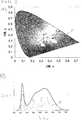
Gemäß
Auch die beiden Farborte C, D liegen auf einer gemeinsamen Verlängerungsgeraden E einer Isothermen I mit einer korrelierten Farbtemperatur im Bereich 2000 K bis 8000 K, bevorzugt im Bereich von 2300 K bis 5000 K und liegen auf unterschiedlichen Seiten der Planck-Kurve P. Ein Abstand der Farborte A, B zur Planck-Kurve P ist näherungsweise gleich. Der Abstand des Farborts D zur Planck-Kurve P ist kleiner als der des Farborts C, der die kleinere cy-Koordinate aufweist. Somit ist durch die Farborte A, B, C, D ein Viereck aufgespannt, in CIE-xy-Darstellung.The two color loci C, D lie on a common extension line E of an isotherm I with a correlated color temperature in the range 2000 K to 8000 K, preferably in the range of 2300 K to 5000 K and lie on different sides of the Planck curve P. A distance the color loci A, B to the Planck curve P is approximately equal. The distance of the color locus D to the Planck curve P is smaller than that of the color locus C, which has the smaller cy coordinate. Thus, a rectangle is spanned by the color loci A, B, C, D, in CIE xy representation.
Die Lichtquellen für die Farborte A, B, C, D werden bevorzugt von baugleichen Halbleiterchips mit einer Wellenlänge maximaler Intensität im Bereich von mindestens 380 nm bis höchstens 480 nm angeregt, wie auch in allen anderen Ausführungsbeispielen möglich. Abweichend hiervon können auch Halbleiterchips mit unterschiedlichen Wellenlängen maximaler Intensität Verwendung finden. Gemäß
Als Leuchtstoffe sind beispielsweise die in der Druckschrift
Der Farbort A kann beispielsweise durch einen Halbleiterchip, der im Bereich von 380 nm bis 480 nm (Peak-Wellenlägen oder Wellenlänge maximaler Intensität) emittiert, und einem oder mehreren Leuchtstoffen im zugehörigen Lichtweg erzeugt werden. Hierfür wird bevorzugt ein Leuchtstoff der Formel Y3(Alx-lGax)5O12:Ce3+ verwendet oder auch eine Mischung von mehreren Leuchtstoffen der Formel Y3(Alx-lGax)5O12:Ce3+. Die Dominanz-Wellenlänge dieses Leuchtstoffmaterials befindet sich insbesondere im Bereich von 572 nm bis 575 nm.The color locus A may be generated, for example, by a semiconductor chip emitting in the range of 380 nm to 480 nm (peak wave length or maximum intensity wavelength) and one or more phosphors in the associated light path. For this purpose, preference is given to using a phosphor of the formula Y3 (Alxl Gax )5 O12 : Ce3+ or else a mixture of a plurality of phosphors of the formula Y3 (Alxl Gax )5 O12 : Ce3+ . The dominant wavelength of this phosphor material is in particular in the range from 572 nm to 575 nm.
Der Farbort dieses Leuchtstoffmaterials (nicht eingezeichnet) liegt, bei einer Anregungswellenlänge von zirka 460 nm, bevorzugt im Bereich von cx = 0,453 bis 0,469 und cy = 0,532 bis 0,520. Alternativ oder zusätzlich kann für den Farbort A auch ein Leuchtstoff der Formel (Luy-l,Yy)3(Alx-1Gax)5O12:Ce3+ verwendet werden oder eine Mischung von mehreren solchen Leuchtstoffen. Die Dominanz-Wellenlänge eines solchen Leuchtstoffmaterials befindet sich bevorzugt (bei einer Anregungswellenlänge von zirka 460 nm) im Bereich von 558 nm bis 562 nm. Der Farbort dieses Leuchtstoffmaterials (nicht eingezeichnet) liegt bevorzugt (Anregungswellenlänge = 460 nm) im Bereich von cx = 0,356 bis 0,374 und cy = 0,561 bis 0,573. Diese Materialien können optional anteilig < 20% noch mit einem der nachfolgenden Leuchtstoffe gemischt werden: Eu2+-dotierte Nitride, beispielsweise (Ca,Sr)AlSiN3:Eu2+, Sr(Ca,Sr)Si2Al2N6:Eu2+, (Sr,Ca)AlSiN3·Si2N2O:Eu2+, (Ca,Ba,Sr)2Si5N8:Eu2+, (Sr,Ca)[LiAl3N4]:Eu2+. Die Dominanz-Wellenlänge des nitridischen Leuchtstoffmaterials befindet sich bevorzugt (Anregungswellenlänge = 460 nm) im Bereich von 590 nm bis 615 nm, besonders bevorzugt im Bereich von 596 nm bis 604 nm. Der Farbort des nitridischen Leuchtstoffmaterials (nicht gezeichnet) liegt beispielsweise (Anregungswellenlänge = 460 nm) im Bereich von cx = 0,608 bis 0,639 und cy = 0,360 bis 0,390.The color locus of this phosphor material (not shown) is, with an excitation wavelength of about 460 nm, preferably in the range of cx = 0.453 to 0.469 and cy = 0.532 to 0.520. Alternatively or additionally, a phosphor of the formula (Luyl , Yy )3 (Alx-1 Gax )5 O12 : Ce3+ or a mixture of a plurality of such phosphors may also be used for the color locus A. The dominant wavelength of such a phosphor material is preferably (at an excitation wavelength of about 460 nm) in the range of 558 nm to 562 nm. The color locus of this phosphor material (not shown) is preferably (excitation wavelength = 460 nm) in the range of cx = 0.356 to 0.374 and cy = 0.561 to 0.573. Optionally <20% of these materials can also be mixed with one of the following phosphors: Eu2+ -doped nitrides, for example (Ca, Sr) AlSiN3 : Eu2+ , Sr (Ca, Sr) Si2 Al2 N6 : Eu2+ , (Sr, Ca) AlSiN3 .Si2 N2 O: Eu2+ , (Ca, Ba, Sr)2 Si5 N8 : Eu2+ , (Sr, Ca) [LiAl3 N4 ] : Eu2+ . The dominant wavelength of the nitride phosphor material is preferably (excitation wavelength = 460 nm) in the range from 590 nm to 615 nm, particularly preferably in the range from 596 nm to 604 nm. The color locus of the nitridic phosphor material (not shown) is, for example, (excitation wavelength 460 nm) in the range of cx = 0.608 to 0.639 and cy = 0.360 to 0.390.
Die Farborte B und C werden zum Beispiel durch einen Halbleiterchip, der im Bereich von 380 nm bis 480 nm (Peak-Wellenlägen) emittiert und dem ein oder mehrere Leuchtstoffe im Lichtweg nachgeordnet sind, erzeugt. Hierfür wird bevorzugt ein Leuchtstoff oder eine Mischung von Leuchtstoffen mit einer Dominanz-Wellenlänge im Bereich von 580 nm bis 650 nm verwendet. Diese Leuchtstoffe können zum Beispiel aus folgenden Materialsystemen ausgewählt sein: Eu2+-dotierte Nitride, beispielsweise (Ca,Sr)AlSiN3:Eu2+, Sr(Ca,Sr)Si2Al2N6:Eu2+, (Sr,Ca)AlSiN3·Si2N2O:Eu2+, (Ca,Ba,Sr)2Si5N8:Eu2+, (Sr,Ca)[LiAl3N4]:Eu2+. Bevorzugt werden diese Leuchtstoffe zusätzlich mit einem grünlichen und/oder gelben Leuchtstoff gemischt, zum Beispiel aus den folgenden Materialsystemen: Lu3(All-xGax)5O12:Ce3+, Y3(Al1-xGax)5O12:Ce3+, Eu2+-dotierte Sulfide, (Ba,Sr,Ca)Si2O2N2:Eu2+, SiAlONe, Nitrido-Orthosilikate wie AE2-x-aRExEuaSi1-yO4-x-2yNx mit RE = Seltenerdmetall und AE = Erdalkalimetall, Orthosilikate wie (Ba,Sr,Ca)2SiO4:Eu2+, Chlorosilikate wie Ca8Mg(SiO4)4Cl2:Eu2+.The color loci B and C are generated, for example, by a semiconductor chip which emits in the range of 380 nm to 480 nm (peak wave lengths) and which is followed by one or more phosphors in the light path. For this purpose, a phosphor or a mixture of phosphors having a dominant wavelength in the range of 580 nm to 650 nm is preferably used. These phosphors may be selected, for example, from the following material systems: Eu2+ -doped nitrides, for example (Ca, Sr) AlSiN3 : Eu2+ , Sr (Ca, Sr) Si2 Al2 N6 : Eu2+ , (Sr , Ca) AlSiN3 .Si2 N2 O: Eu2+ , (Ca, Ba, Sr)2 Si5 N8 : Eu2+ , (Sr, Ca) [LiAl3 N4 ]: Eu2+ . These phosphors are preferably additionally mixed with a greenish and / or yellow phosphor, for example, from the following material systems: Lu3 (Allx Gax)5 O12: Ce3+, Y3 (Al1-x Gax)5 O12 : Ce3+ , Eu2+ -doped sulfides, (Ba, Sr, Ca) Si2 O2 N2 : Eu2+ , SiAlONs, nitrido-orthosilicates such as AE2-xa REx Eua Si1-y O4-x-2y Nx with RE = rare earth metal and AE = alkaline earth metal, orthosilicates such as (Ba, Sr, Ca)2 SiO4 : Eu2+ , chlorosilicates such as Ca8 Mg (SiO4 )4 Cl2 : Eu2+ .
Der Farbort D kann beispielsweise durch einen Halbleiterchip, der im Bereich von 380 nm bis 480 nm (Peak-Wellenlägen) emittiert, zusammen mit einem oder mehreren Leuchtstoffen im Lichtweg, erzeugt werden. Hierfür wird etwa ein Y3(Al1-xGax)5O12:Ce3+ verwendet oder eine Mischung von mehreren solche Leuchtstoffen. Die Dominanz-Wellenlänge dieses Leuchtstoffmaterials befindet sich bevorzugt (Anregungswellenlänge = 460 nm) im Bereich von 572 nm bis 575 nm. Der Farbort dieses Leuchtstoffmaterials (nicht gezeichnet) liegt bevorzugt (Anregungswellenlänge = 460 nm) im Bereich von cx = 0,453 bis 0,469 und cy = 0,532 bis 0,520. Alternativ oder zusätzlich kann auch ein (Lu1-y,Yy)3(Al1-xGax)5O12:Ce3+ verwendet werden oder eine Mischung von mehreren solchen Leuchtstoffen. Die Dominanz-Wellenlänge des Leuchtstoffmaterials befindet sich bevorzugt (Anregungswellenlänge = 460 nm) im Bereich von 558 nm bis 562 nm. Der Farbort des Leuchtstoffmaterials (nicht gezeichnet) liegt dann bevorzugt (Anregungswellenlänge = 460 nm) im Bereich von cx = 0,356 bis 0,374 und cy = 0,561 bis 0,573. Diese Materialien werden zum Beispiel mit einem oder mehrerer Leuchtstoffe dieser Materialklassen gemischt: Eu2+-dotierte Nitride wie (Ca,Sr)AlSiN3:Eu2+, Sr(Ca,Sr)Si2Al2N6:Eu2+, (Sr,Ca)AlSiN3·Si2N2O:Eu2+, (Ca,Ba,Sr)2Si5N8:Eu2+, (Sr,Ca)[LiAl3N4]:Eu2+. Die Dominanz-Wellenlänge des nitridischen Leuchtstoffmaterials befindet sich bevorzugt (Anregungswellenlänge = 460 nm) im Bereich von 590 nm bis 615 nm oder 596 nm bis 604 nm. Der Farbort des nitridischen Leuchtstoffmaterials liegt beispielsweise (Anregungswellenlänge = 460 nm) im Bereich von cx = 0,608 bis 0,639 und cy = 0,360 bis 0,390. The color locus D may be generated, for example, by a semiconductor chip emitting in the range of 380 nm to 480 nm (peak wavelengths) together with one or more phosphors in the light path. For this purpose, about a Y3 (Al1-x Gax )5 O12 : Ce3+ used or a mixture of several such phosphors. The dominant wavelength of this phosphor material is preferably (excitation wavelength = 460 nm) in the range of 572 nm to 575 nm. The color locus of this phosphor material (not shown) is preferably (excitation wavelength = 460 nm) in the range of cx = 0.453 to 0.469 and cy = 0.532 to 0.520. Alternatively or additionally, it is also possible to use a (Lu1-y , Yy )3 (Al1-x Gax )5 O12 : Ce3+ or a mixture of a plurality of such phosphors. The dominant wavelength of the phosphor material is preferably (excitation wavelength = 460 nm) in the range of 558 nm to 562 nm. The color location of the phosphor material (not shown) is then preferred (excitation wavelength = 460 nm) in the range of cx = 0.356 to 0.374 and cy = 0.561 to 0.573. These materials are mixed, for example, with one or more phosphors of these classes of materials: Eu2+ -doped nitrides such as (Ca, Sr) AlSiN3 : Eu2+ , Sr (Ca, Sr) Si2 Al2 N6 : Eu2+ , (Sr, Ca) AlSiN3 .Si2 N2 O: Eu2+ , (Ca, Ba, Sr)2 Si5 N8 : Eu2+ , (Sr, Ca) [LiAl3 N4 ]: Eu2+ , The dominant wavelength of the nitride phosphor material is preferably (excitation wavelength = 460 nm) in the range of 590 nm to 615 nm or 596 nm to 604 nm. The color locus of the nitride phosphor material is for example (excitation wavelength = 460 nm) in the range of cx = 0.608 to 0.639 and cy = 0.360 to 0.390.
Die in den Figuren dargestellten Farborte A, B, C, D können jeweils mit einer Toleranz von höchstens 0,05 Einheiten oder 0,03 Einheiten hinsichtlich ihrer CIE-x-Koordinaten und CIE-y-Koordinaten in der CIE-xy-Darstellung verwendet werden, siehe auch die Tabelle in
Gemäß der
Der Farbort D liegt innerhalb eines Dreiecks, das durch die drei Farborte A, B, C aufgespannt ist, die abseits der Planck-Kurve P liegen. Es können beispielsweise entweder zwei Farborte bei einem kleineren cy und ein Farbort bei einem größeren cy als bei dem Farbort D auf der Planck-Kurve P gewählt werden. Alternativ können auch zwei Farborte bei einem größeren cy als der Farbort D auf der Planck-Kurve P liegen. Ein Vorteil einer solchen Ausgestaltung der Farborte A, B, C, D liegt darin, dass auch beim Betrieb von nur einer Lichtquelle, insbesondere der mit dem Farbort D, ein Farbort der Gesamtstrahlung auf der Planck-Kurve P erreicht werden kann und somit einfach die Emission von weißem Licht betreibbar ist.The color locus D lies within a triangle which is spanned by the three color loci A, B, C, which lie apart from the Planck curve P. For example, either two color loci at a smaller cy and one color locus at a larger cy than at the color locus D on the Planck curve P can be selected. Alternatively, two color loci may be located at a larger cy than the color locus D on the Planck curve P. An advantage of such an embodiment of the color loci A, B, C, D is that even when operating only one light source, in particular the one with the color locus D, a color location of the total radiation on the Planck curve P can be achieved and thus simply the Emission of white light is operable.
Es können alle Farborte, insbesondere alle Farborte auf der Planck-Kurve P, innerhalb des durch die Farborte A, B, C aufgespannten Dreiecks erreicht werden. Der Farbort D auf der Planck-Kurve P liegt bevorzugt bei mindestens 2300 K oder 3000 K und/oder bei höchstens 6000 K oder 8500 K. Anders als dargestellt können die sich nicht auf der Planck-Kurve P liegenden Farborte A, B, D auch in Bereichen im CIE-xy-Diagramm befinden, die weiter von dem Farbort D entfernt liegen als gezeichnet. Im Prinzip sind die Farborte der Punkte A, B, C dann beliebig wählbar. Bevorzugt liegen in den Ausführungsbeispielen der
In den Ausführungsbeispielen gemäß
Es können auch zwei der Farborte bei einem kleineren cy und ein Farbort bei einem größeren cy als der Farbort D auf der Planck-Kurve P liegen, anders als in den
Im gemeinsamen Betrieb können alle Farborte innerhalb des durch die vier Farborte aufgespannten Vierecks erreicht werden. Der Farbort auf der Planck-Kurve P liegt bevorzugt bei mindestens 2300 K oder 3000 K und/oder bei höchstens 6000 K oder 8500 K.In joint operation, all color locations can be achieved within the rectangle spanned by the four color loci. The color locus on the Planck curve P is preferably at least 2300 K or 3000 K and / or at most 6000 K or 8500 K.
Typische cx-cy-Koordinaten der einzelnen Farborte sind beispielsweise: Farbort A: 0,322/0,336; Farbort B: 0,55/0,24; Farbort C: 0,45/0,47; Farbort D: 0,50/0,35. Unter typisch versteht man hier beispielsweise eine Abweichung +/– kleiner als 0,05 oder 0,03 oder 0,01. Farbort A kann beispielsweise als Kombination eines blaues Licht emittierenden Halbleiterchips mit einer Leuchtstoffmischung realisiert werden, wobei die Leuchtstoffmischung bezüglich der Wellenlängenumwandlung bevorzugt mit mehr als 90 % auf einem (Lu,Y)3(Al1-xGax)5O12:Ce3+-Material oder eine Mischung von mehreren solcher Materialien basiert.Typical cx -cy coordinates of the individual color loci are, for example: Color locus A: 0.322 / 0.336; Color location B: 0.55 / 0.24; Color location C: 0.45 / 0.47; Color location D: 0.50 / 0.35. Under typical one understands here for example, a deviation +/- less than 0.05 or 0.03 or 0.01. Color locus A can be realized, for example, as a combination of a blue light-emitting semiconductor chip with a phosphor mixture, wherein the phosphor mixture with respect to the wavelength conversion preferably with more than 90% on a (Lu, Y)3 (Al1-x Gax )5 O12 : Ce3+ material or a mixture of several such materials.
Die Farborte B, C, D werden bevorzugt durch eine Mischung von einem oder mehreren Leuchtstoffen mit einer Dominanz-Wellenlänge im Bereich von 580 nm bis 650 nm realisiert. Solche Leuchtstoffe können etwa aus folgenden Materialsystemen ausgewählt sein: Eu2+-dotierte Nitride wie (Ca,Sr)AlSiN3:Eu2+, Sr(Ca,Sr)Si2Al2N6:Eu2+, (Sr,Ca)AlSiN3·Si2N2O:Eu2+, (Ca,Ba,Sr)2Si5N8:Eu2+, (Sr,Ca)[LiAl3N4]:Eu2+. Die Dominanz-Wellenlänge des nitridischen Leuchtstoffmaterials befindet sich bevorzugt (Anregungswellenlänge = 460 nm) im Bereich von 590 nm bis 615 nm, besonders bevorzugt im Bereich von 596 nm bis 604 nm. Der Farbort des nitridischen Leuchtstoffmaterials (nicht gezeichnet) liegt beispielsweise (Anregungswellenlänge = 460 nm) im Bereich von cx = 0,608 bis 0,639 und cy = 0,360 bis 0,390. Bevorzugt werden diese Leuchtstoffe zusätzlich mit einem grünlichen und oder gelben Leuchtstoff gemischt, die zum Beispiel aus den folgenden Materialsystemen ausgewählt sind: (Lu1-y,Yy)3(Al1-xGax)5O12:Ce3+. Die Dominanz-Wellenlänge dieses Leuchtstoffmaterials befindet sich bevorzugt (Anregungswellenlänge = 460 nm) im Bereich von 572 nm bis 575 nm. Der Farbort dieses Leuchtstoffmaterials (nicht gezeichnet) liegt bevorzugt (Anregungswellenlänge = 460 nm) im Bereich von cx = 0,453 bis 0.469 und cy = 0,532 bis 0,520.The color loci B, C, D are preferably realized by a mixture of one or more phosphors having a dominant wavelength in the range from 580 nm to 650 nm. Such phosphors may be selected from, for example, the following material systems: Eu2+ -doped nitrides such as (Ca, Sr) AlSiN3 : Eu2+ , Sr (Ca, Sr) Si2 Al2 N6 : Eu2+ , (Sr, Ca ) AlSiN3 .Si2 N2 O: Eu2+ , (Ca, Ba, Sr)2 Si5 N8 : Eu2+ , (Sr, Ca) [LiAl3 N4 ]: Eu2+ . The dominant wavelength of the nitride phosphor material is preferably (excitation wavelength = 460 nm) in the range from 590 nm to 615 nm, particularly preferably in the range from 596 nm to 604 nm. The color locus of the nitridic phosphor material (not shown) is, for example, (excitation wavelength 460 nm) in the range of cx = 0.608 to 0.639 and cy = 0.360 to 0.390. These phosphors are preferably additionally mixed with a greenish and/ or yellow phosphor which are selected, for example, from the following material systems: (Lu1-y , Yy )3 (Al1-x Gax )5 O12 : Ce3+ . The dominant wavelength of this phosphor material is preferably (excitation wavelength = 460 nm) in the range of 572 nm to 575 nm. The color locus of this phosphor material (not shown) is preferably (excitation wavelength = 460 nm) in the range of cx = 0.453 to 0.469 and cy = 0.532 to 0.520.
In
In den Ausführungsbeispielen der
Es liegt beispielsweise ein Farborte bei einem kleineren cy und ein Farbort bei einem größeren cy als einer oder beide Lichtquellen mit dem Farbort auf der Planck-Kurve P. Beide Farborte A, B, die auf der Verlängerungsgeraden liegen, können dabei eine cx-Koordinate zwischen den beiden Farborten auf der Planck-Kurve P aufweisen, siehe
Ein Vorteil der Ausführungsbeispiele der
Bevorzugt liegen in den Ausführungsbeispielen der
Das Ausführungsbeispiel, wie in
Als Leuchtstoffmaterial kann alternativ oder zusätzlich zu den unter
Die zugehörigen Emissionsspektren der Lichtquellen für die Farborte A, B, C, D sind in
Im Ausführungsbeispiel gemäß
Es können beispielsweise entweder zwei Farborte bei einem kleineren cy und ein Farbort bei einem größeren cy als die Planck-Kurve P gewählt werden oder auch zwei Farborte bei einem größeren cy als die Planck-Kurve P. Im gemeinsamen Betrieb können alle Farborte innerhalb des aufgespannten Dreiecks oder Vierecks erreicht werden. Ein Vorteil an diesem Ausführungsbeispiel ist, dass infrarotes Licht bei einer Fotographie nach dem Aussenden von Objekten reflektiert werden kann und von einem Detektor wie einem Kameramodul wieder detektiert werden kann, wodurch sich Informationen bezüglich einer dreidimensionalen Anordnung der fotografierten Objekte erhalten lassen.For example, either two color loci at a smaller cy and one color locus at a larger cy can be chosen as the Planck curve P or two color loci at a larger cy than the Planck curve P. In joint operation, all color loci within of the spanned triangle or quadrilateral. An advantage of this embodiment is that infrared light can be reflected in a photograph after the emission of objects and can be detected again by a detector such as a camera module, whereby information regarding a three-dimensional arrangement of the photographed objects can be obtained.
Es können in
In
Die hier beschriebene Erfindung ist nicht durch die Beschreibung anhand der Ausführungsbeispiele beschränkt. Vielmehr umfasst die Erfindung jedes neue Merkmal sowie jede Kombination von Merkmalen, was insbesondere jede Kombination von Merkmalen in den Patentansprüchen beinhaltet, auch wenn dieses Merkmal oder diese Kombination selbst nicht explizit in den Patentansprüchen oder Ausführungsbeispielen angegeben ist.The invention described here is not limited by the description based on the embodiments. Rather, the invention encompasses any novel feature as well as any combination of features, including in particular any combination of features in the claims, even if this feature or combination itself is not explicitly stated in the patent claims or exemplary embodiments.
BezugszeichenlisteLIST OF REFERENCE NUMBERS
- 11
- optoelektronisches Halbleiterbauteil optoelectronic semiconductor device
- 22
- Träger carrier
- 33
- Verguss grouting
- 44
- Optik optics
- 1010
- optoelektronischer Halbleiterchip optoelectronic semiconductor chip
- 11, 12, 13, 1411, 12, 13, 14
- Lichtquellen light sources
- 21, 22, 23, 24, 2521, 22, 23, 24, 25
- Leuchtstoffmischung Phosphor mixture
- A, B, C, DA, B, C, D
- Farborte in der CIE-Normfarbtafel Color locations in the CIE standard color chart
- CCTCCT
- korrelierte Farbtemperatur correlated color temperature
- Ee
- Verlängerungsgerade einer Isothermen Extension line of an isotherm
- II
- Isotherme isotherm
- PP
- Planck-Kurve in der CIE-Normfarbtafel Planck curve in the CIE standard color chart
- SS
- Intensität in willkürliche Einheiten Intensity in arbitrary units
- u, v, x, yu, v, x, y
- Koordinaten in der CIE-Normfarbtafel Coordinates in the CIE standard color chart
- λλ
- Wellenlänge in nm Wavelength in nm
ZITATE ENTHALTEN IN DER BESCHREIBUNG QUOTES INCLUDE IN THE DESCRIPTION
Diese Liste der vom Anmelder aufgeführten Dokumente wurde automatisiert erzeugt und ist ausschließlich zur besseren Information des Lesers aufgenommen. Die Liste ist nicht Bestandteil der deutschen Patent- bzw. Gebrauchsmusteranmeldung. Das DPMA übernimmt keinerlei Haftung für etwaige Fehler oder Auslassungen.This list of the documents listed by the applicant has been generated automatically and is included solely for the better information of the reader. The list is not part of the German patent or utility model application. The DPMA assumes no liability for any errors or omissions.
Zitierte PatentliteraturCited patent literature
- US 2003/0095138 A1[0006]US 2003/0095138 A1[0006]
- EP 2549330 A1[0059]EP 2549330 A1[0059]
Zitierte Nicht-PatentliteraturCited non-patent literature
- Y. Ohno, „Calculation of CCT and Duv and practical conversion formula“, CORM-Konferenz 2011, Gaversburg, Maryland, USA, 03.–05. Mai 2011[0006]Y. Ohno, "Calculation of CCT and Duv and practical conversion formula", CORM Conference 2011, Gaversburg, Maryland, USA, 03.-05. May 2011[0006]
- Ohno, Seite 5[0007]Oh no, page 5[0007]
- M. Wood, „MacAdam Ellipses“, ESTA Protocol Magazine, Herbst 2010, Seiten 15 bis 18[0008]M. Wood, "MacAdam Ellipses", ESTA Protocol Magazine, Fall 2010, pages 15 to 18[0008]
Claims (15)
Translated fromGermanPriority Applications (7)
| Application Number | Priority Date | Filing Date | Title |
|---|---|---|---|
| DE102014112681.5ADE102014112681A1 (en) | 2014-09-03 | 2014-09-03 | Optoelectronic semiconductor device and flashlight |
| US15/508,511US10020292B2 (en) | 2014-09-03 | 2015-08-27 | Optoelectronic semiconductor component and flashlight |
| CN201580047698.5ACN106796935B (en) | 2014-09-03 | 2015-08-27 | Optoelectronic semiconductor components and flash lamps |
| JP2017512681AJP6695327B2 (en) | 2014-09-03 | 2015-08-27 | Optoelectronic semiconductor device and flashlight |
| DE112015004033.1TDE112015004033B4 (en) | 2014-09-03 | 2015-08-27 | Optoelectronic semiconductor component and flash light |
| PCT/EP2015/069605WO2016034480A1 (en) | 2014-09-03 | 2015-08-27 | Optoelectronic semiconductor component and flashlight |
| TW104128772ATWI621283B (en) | 2014-09-03 | 2015-09-01 | Photoelectric semiconductor components and flash |
Applications Claiming Priority (1)
| Application Number | Priority Date | Filing Date | Title |
|---|---|---|---|
| DE102014112681.5ADE102014112681A1 (en) | 2014-09-03 | 2014-09-03 | Optoelectronic semiconductor device and flashlight |
Publications (1)
| Publication Number | Publication Date |
|---|---|
| DE102014112681A1true DE102014112681A1 (en) | 2016-03-03 |
Family
ID=54007721
Family Applications (2)
| Application Number | Title | Priority Date | Filing Date |
|---|---|---|---|
| DE102014112681.5AWithdrawnDE102014112681A1 (en) | 2014-09-03 | 2014-09-03 | Optoelectronic semiconductor device and flashlight |
| DE112015004033.1TActiveDE112015004033B4 (en) | 2014-09-03 | 2015-08-27 | Optoelectronic semiconductor component and flash light |
Family Applications After (1)
| Application Number | Title | Priority Date | Filing Date |
|---|---|---|---|
| DE112015004033.1TActiveDE112015004033B4 (en) | 2014-09-03 | 2015-08-27 | Optoelectronic semiconductor component and flash light |
Country Status (6)
| Country | Link |
|---|---|
| US (1) | US10020292B2 (en) |
| JP (1) | JP6695327B2 (en) |
| CN (1) | CN106796935B (en) |
| DE (2) | DE102014112681A1 (en) |
| TW (1) | TWI621283B (en) |
| WO (1) | WO2016034480A1 (en) |
Cited By (5)
| Publication number | Priority date | Publication date | Assignee | Title |
|---|---|---|---|---|
| DE102016104875A1 (en)* | 2016-03-16 | 2017-09-21 | Osram Opto Semiconductors Gmbh | Optoelectronic component, method for producing an optoelectronic component and flash lighting for a portable device |
| WO2018050921A1 (en)* | 2016-09-19 | 2018-03-22 | Osram Opto Semiconductors Gmbh | Light-emitting device |
| DE102017103884A1 (en) | 2017-02-24 | 2018-08-30 | Osram Opto Semiconductors Gmbh | Lighting device, electronic device with a lighting device and use of a lighting device |
| JP2019510377A (en)* | 2016-03-24 | 2019-04-11 | ティーディーケイ・エレクトロニクス・アクチェンゲゼルシャフトTdk Electronics Ag | Multi LED system |
| WO2020030505A1 (en)* | 2018-08-09 | 2020-02-13 | Osram Oled Gmbh | Optoelectronic component emitting visible light and ir radiation |
Families Citing this family (22)
| Publication number | Priority date | Publication date | Assignee | Title |
|---|---|---|---|---|
| EP3214359B1 (en)* | 2014-10-28 | 2021-12-15 | Seoul Semiconductor Co., Ltd. | White light source and white light source system |
| US11296058B2 (en) | 2017-02-27 | 2022-04-05 | Juganu, Ltd. | Tunable white lighting systems |
| US10700245B2 (en) | 2017-07-04 | 2020-06-30 | Nichia Corporation | Light-emitting device |
| US11257990B2 (en) | 2017-09-29 | 2022-02-22 | Nichia Corporation | Light emitting device |
| JP6705476B2 (en)* | 2017-09-29 | 2020-06-03 | 日亜化学工業株式会社 | Light emitting device |
| DE102017122936A1 (en) | 2017-10-04 | 2019-04-04 | Osram Opto Semiconductors Gmbh | Optoelectronic component |
| KR102516217B1 (en)* | 2017-11-30 | 2023-04-03 | 서울반도체 주식회사 | Light-emitting apparatus including light-emitting diodes |
| WO2019126000A1 (en)* | 2017-12-22 | 2019-06-27 | Lumileds Llc | Porous micron-sized particles to tune light scattering |
| US10761246B2 (en) | 2017-12-22 | 2020-09-01 | Lumileds Llc | Light emitting semiconductor device having polymer-filled sub-micron pores in porous structure to tune light scattering |
| JP6665872B2 (en)* | 2018-01-15 | 2020-03-13 | 日亜化学工業株式会社 | Light emitting device and method of manufacturing light emitting device |
| US10349484B1 (en)* | 2018-05-31 | 2019-07-09 | Cree, Inc. | Solid state lighting devices with reduced melatonin suppression characteristics |
| TWI675239B (en)* | 2018-08-13 | 2019-10-21 | 友達光電股份有限公司 | Display device |
| WO2020055119A1 (en)* | 2018-09-12 | 2020-03-19 | 서울반도체주식회사 | Light-emitting device |
| JP6959548B2 (en) | 2018-10-04 | 2021-11-02 | 日亜化学工業株式会社 | Light emitting device and its manufacturing method |
| JP7248939B2 (en)* | 2018-10-12 | 2023-03-30 | 日亜化学工業株式会社 | light emitting device |
| JP7089181B2 (en) | 2018-10-12 | 2022-06-22 | 日亜化学工業株式会社 | Light emitting device |
| WO2020114463A1 (en)* | 2018-12-07 | 2020-06-11 | 海迪科(南通)光电科技有限公司 | Packaging body and preparation method therefor |
| CN112203377B (en)* | 2019-06-21 | 2023-04-14 | 四川联恺照明有限公司 | A color temperature adjustment method, a color temperature adjustment device and a light source assembly |
| JP7323787B2 (en) | 2019-07-31 | 2023-08-09 | 日亜化学工業株式会社 | Lighting device and lighting device with infrared camera |
| DE102019125268A1 (en)* | 2019-09-19 | 2021-03-25 | OSRAM Opto Semiconductors Gesellschaft mit beschränkter Haftung | OPERATING PROCEDURE FOR AN OPTOELECTRONIC SEMICONDUCTOR COMPONENT AND OPTOELECTRONIC SEMICONDUCTOR COMPONENT |
| CN111766712B (en)* | 2020-07-23 | 2022-02-01 | 深圳市锐思华创技术有限公司 | Laser scanning projection module with high brightness, wide color gamut and low light spot |
| WO2023083708A1 (en)* | 2021-11-09 | 2023-05-19 | Signify Holding B.V. | High frequency wavelength sweeping laser for imitating continuous emission with tunable intensity profile |
Citations (5)
| Publication number | Priority date | Publication date | Assignee | Title |
|---|---|---|---|---|
| US20030095138A1 (en) | 2001-10-15 | 2003-05-22 | Samsung Electronics Co., Ltd | Color temperature conversion system and method using the same |
| US20060082679A1 (en)* | 2004-10-14 | 2006-04-20 | Chua Janet B Y | Electronic flash, imaging device and method for producing a flash of light having a wavelength spectrum in the visible range and the infrared range using a fluorescent material |
| US20060126326A1 (en)* | 2004-12-15 | 2006-06-15 | Ng Kee Y | Light-emitting diode flash module with enhanced spectral emission |
| US20120326627A1 (en)* | 2011-06-14 | 2012-12-27 | Luminus Devices, Inc. | Systems and methods for controlling white light |
| EP2549330A1 (en) | 2006-05-05 | 2013-01-23 | Prysm, Inc. | Phosphor compositions and other fluorescent materials for display systems and devices |
Family Cites Families (13)
| Publication number | Priority date | Publication date | Assignee | Title |
|---|---|---|---|---|
| US6414426B1 (en)* | 1997-02-13 | 2002-07-02 | Matsushita Electric Industrial Co., Ltd. | High-efficiency light source |
| JP2008218486A (en)* | 2007-02-28 | 2008-09-18 | Toshiba Lighting & Technology Corp | Light emitting device |
| JP2008283155A (en)* | 2007-05-14 | 2008-11-20 | Sharp Corp | Light emitting device, lighting device, and liquid crystal display device |
| US8339029B2 (en) | 2009-02-19 | 2012-12-25 | Cree, Inc. | Light emitting devices and systems having tunable chromaticity |
| DE102009015313B4 (en) | 2009-03-27 | 2022-02-24 | OSRAM Opto Semiconductors Gesellschaft mit beschränkter Haftung | display device |
| US8426871B2 (en)* | 2009-06-19 | 2013-04-23 | Honeywell International Inc. | Phosphor converting IR LEDs |
| FR2956407B1 (en) | 2010-02-17 | 2013-03-08 | Saint Gobain | LUMINESCENT COMPOUNDS |
| US8411025B2 (en)* | 2010-04-10 | 2013-04-02 | Lg Innotek Co., Ltd. | Lighting apparauts |
| EP2558893A4 (en)* | 2010-04-16 | 2014-06-11 | Flex Lighting Ii Llc | TEACH COMPRISING A LIGHT GUIDE BASED ON A FILM |
| JP2012199218A (en) | 2010-09-09 | 2012-10-18 | Mitsubishi Chemicals Corp | Light emitting device, illumination system, and illumination method |
| CN102458019B (en)* | 2010-10-26 | 2014-01-22 | 财团法人工业技术研究院 | Light color modulation method and light emitting diode light source module |
| US8870617B2 (en)* | 2013-01-03 | 2014-10-28 | Xicato, Inc. | Color tuning of a multi-color LED based illumination device |
| WO2016093076A1 (en)* | 2014-12-09 | 2016-06-16 | 信越化学工業株式会社 | Wavelength conversion member and light-emitting device |
- 2014
- 2014-09-03DEDE102014112681.5Apatent/DE102014112681A1/ennot_activeWithdrawn
- 2015
- 2015-08-27CNCN201580047698.5Apatent/CN106796935B/enactiveActive
- 2015-08-27DEDE112015004033.1Tpatent/DE112015004033B4/enactiveActive
- 2015-08-27USUS15/508,511patent/US10020292B2/enactiveActive
- 2015-08-27WOPCT/EP2015/069605patent/WO2016034480A1/enactiveApplication Filing
- 2015-08-27JPJP2017512681Apatent/JP6695327B2/enactiveActive
- 2015-09-01TWTW104128772Apatent/TWI621283B/enactive
Patent Citations (5)
| Publication number | Priority date | Publication date | Assignee | Title |
|---|---|---|---|---|
| US20030095138A1 (en) | 2001-10-15 | 2003-05-22 | Samsung Electronics Co., Ltd | Color temperature conversion system and method using the same |
| US20060082679A1 (en)* | 2004-10-14 | 2006-04-20 | Chua Janet B Y | Electronic flash, imaging device and method for producing a flash of light having a wavelength spectrum in the visible range and the infrared range using a fluorescent material |
| US20060126326A1 (en)* | 2004-12-15 | 2006-06-15 | Ng Kee Y | Light-emitting diode flash module with enhanced spectral emission |
| EP2549330A1 (en) | 2006-05-05 | 2013-01-23 | Prysm, Inc. | Phosphor compositions and other fluorescent materials for display systems and devices |
| US20120326627A1 (en)* | 2011-06-14 | 2012-12-27 | Luminus Devices, Inc. | Systems and methods for controlling white light |
Non-Patent Citations (3)
| Title |
|---|
| M. Wood, "MacAdam Ellipses", ESTA Protocol Magazine, Herbst 2010, Seiten 15 bis 18 |
| Ohno, Seite 5 |
| Y. Ohno, "Calculation of CCT and Duv and practical conversion formula", CORM-Konferenz 2011, Gaversburg, Maryland, USA, 03.-05. Mai 2011 |
Cited By (11)
| Publication number | Priority date | Publication date | Assignee | Title |
|---|---|---|---|---|
| DE102016104875A1 (en)* | 2016-03-16 | 2017-09-21 | Osram Opto Semiconductors Gmbh | Optoelectronic component, method for producing an optoelectronic component and flash lighting for a portable device |
| US10629784B2 (en) | 2016-03-16 | 2020-04-21 | Osram Oled Gmbh | Optoelectronic component, method for producing an optoelectronic component and flashlight for a portable device |
| JP2019510377A (en)* | 2016-03-24 | 2019-04-11 | ティーディーケイ・エレクトロニクス・アクチェンゲゼルシャフトTdk Electronics Ag | Multi LED system |
| US10818641B2 (en) | 2016-03-24 | 2020-10-27 | Epcos Ag | Multi-LED system |
| WO2018050921A1 (en)* | 2016-09-19 | 2018-03-22 | Osram Opto Semiconductors Gmbh | Light-emitting device |
| CN109716545A (en)* | 2016-09-19 | 2019-05-03 | 欧司朗光电半导体有限公司 | Luminaire |
| US11201141B2 (en) | 2016-09-19 | 2021-12-14 | Osram Oled Gmbh | Light emitting device |
| CN109716545B (en)* | 2016-09-19 | 2022-04-01 | 欧司朗光电半导体有限公司 | Light emitting device |
| DE102017103884A1 (en) | 2017-02-24 | 2018-08-30 | Osram Opto Semiconductors Gmbh | Lighting device, electronic device with a lighting device and use of a lighting device |
| US11288502B2 (en) | 2017-02-24 | 2022-03-29 | Osram Oled Gmbh | Illumination system, electronic device comprising an illumination system and use of an illumination system |
| WO2020030505A1 (en)* | 2018-08-09 | 2020-02-13 | Osram Oled Gmbh | Optoelectronic component emitting visible light and ir radiation |
Also Published As
| Publication number | Publication date |
|---|---|
| CN106796935B (en) | 2019-09-27 |
| US20170278829A1 (en) | 2017-09-28 |
| WO2016034480A1 (en) | 2016-03-10 |
| DE112015004033A5 (en) | 2017-05-24 |
| CN106796935A (en) | 2017-05-31 |
| TW201624771A (en) | 2016-07-01 |
| TWI621283B (en) | 2018-04-11 |
| JP6695327B2 (en) | 2020-05-20 |
| US10020292B2 (en) | 2018-07-10 |
| JP2017531315A (en) | 2017-10-19 |
| DE112015004033B4 (en) | 2020-08-20 |
Similar Documents
| Publication | Publication Date | Title |
|---|---|---|
| DE112015004033B4 (en) | Optoelectronic semiconductor component and flash light | |
| DE102018123672B4 (en) | white light illuminating device | |
| DE112014002897B4 (en) | Arrangement and method for generating mixed light | |
| DE102010012423A1 (en) | Luminescence diode arrangement, backlighting device and display device | |
| WO2016180930A1 (en) | Radiation-emitting optoelectronic component | |
| DE102008050643A1 (en) | Lamp | |
| DE102014112394B4 (en) | LED light for background light | |
| EP2912688A1 (en) | Light-emitting diode module | |
| DE102009047789A1 (en) | Mixed light source | |
| DE102011013504B4 (en) | Light Emitting Device | |
| DE102015120775B4 (en) | Optoelectronic component and backlight for a display | |
| DE102012101412A1 (en) | Optoelectronic semiconductor device for use as flash-unit in e.g. mobile telephone, has two chips arranged downstream of two conversion elements, respectively, where color temperature of light emitted from device is adjustable | |
| AT14515U1 (en) | LED module with high color rendering index | |
| DE102010046300A1 (en) | lighting module | |
| WO2017158052A1 (en) | Optoelectronic component, method for producing an optoelectronic component and flashlight for a portable device | |
| DE102016123971B4 (en) | Optoelectronic component | |
| DE102010041236A1 (en) | Optoelectronic semiconductor component | |
| DE102018120073B4 (en) | OPTOELECTRONIC SEMICONDUCTOR DEVICE AND FLASHING LIGHT | |
| DE102019122925A1 (en) | Broadband emitter for electromagnetic radiation | |
| EP2997609B1 (en) | White light led module for object lighting | |
| DE102014108004A1 (en) | Method for producing an optoelectronic component and optoelectronic component | |
| DE102017130136A1 (en) | Optoelectronic semiconductor component | |
| AT16507U1 (en) | lighting device | |
| WO2020074389A1 (en) | Optoelectronic semiconductor component and operating method for an optoelectronic semiconductor component | |
| DE202011106595U1 (en) | LED lighting device with high color rendering |
Legal Events
| Date | Code | Title | Description |
|---|---|---|---|
| R163 | Identified publications notified | ||
| R082 | Change of representative | ||
| R118 | Application deemed withdrawn due to claim for domestic priority |