DE102014101556A1 - Optoelectronic component and method for its production - Google Patents
Optoelectronic component and method for its productionDownload PDFInfo
- Publication number
- DE102014101556A1 DE102014101556A1DE102014101556.8ADE102014101556ADE102014101556A1DE 102014101556 A1DE102014101556 A1DE 102014101556A1DE 102014101556 ADE102014101556 ADE 102014101556ADE 102014101556 A1DE102014101556 A1DE 102014101556A1
- Authority
- DE
- Germany
- Prior art keywords
- solder
- contact surface
- chip
- housing
- optoelectronic component
- Prior art date
- Legal status (The legal status is an assumption and is not a legal conclusion. Google has not performed a legal analysis and makes no representation as to the accuracy of the status listed.)
- Pending
Links
- 230000005693optoelectronicsEffects0.000titleclaimsabstractdescription127
- 238000000034methodMethods0.000titleclaimsdescription18
- 238000004519manufacturing processMethods0.000titleclaimsdescription9
- 229910000679solderInorganic materials0.000claimsabstractdescription141
- 239000004065semiconductorSubstances0.000claimsabstractdescription55
- 239000000463materialSubstances0.000claimsdescription16
- 238000004382pottingMethods0.000claimsdescription13
- 238000005476solderingMethods0.000claimsdescription10
- 238000001746injection mouldingMethods0.000claimsdescription4
- 229910052594sapphireInorganic materials0.000claimsdescription3
- 239000010980sapphireSubstances0.000claimsdescription3
- 230000005670electromagnetic radiationEffects0.000description10
- 239000002245particleSubstances0.000description6
- 239000004020conductorSubstances0.000description3
- 230000000694effectsEffects0.000description3
- 239000012777electrically insulating materialSubstances0.000description2
- 238000000465mouldingMethods0.000description2
- 239000004033plasticSubstances0.000description2
- 239000000853adhesiveSubstances0.000description1
- 230000001070adhesive effectEffects0.000description1
- 230000001419dependent effectEffects0.000description1
- 238000011161developmentMethods0.000description1
- 230000018109developmental processEffects0.000description1
- 238000010292electrical insulationMethods0.000description1
- 239000003822epoxy resinSubstances0.000description1
- 239000011440groutSubstances0.000description1
- 239000002184metalSubstances0.000description1
- 230000003287optical effectEffects0.000description1
- 229920000647polyepoxidePolymers0.000description1
- 229920001296polysiloxanePolymers0.000description1
- 238000002360preparation methodMethods0.000description1
- 230000003595spectral effectEffects0.000description1
Images

Classifications
- H—ELECTRICITY
- H10—SEMICONDUCTOR DEVICES; ELECTRIC SOLID-STATE DEVICES NOT OTHERWISE PROVIDED FOR
- H10H—INORGANIC LIGHT-EMITTING SEMICONDUCTOR DEVICES HAVING POTENTIAL BARRIERS
- H10H20/00—Individual inorganic light-emitting semiconductor devices having potential barriers, e.g. light-emitting diodes [LED]
- H10H20/80—Constructional details
- H10H20/81—Bodies
- H10H20/814—Bodies having reflecting means, e.g. semiconductor Bragg reflectors
- H10H20/8142—Bodies having reflecting means, e.g. semiconductor Bragg reflectors forming resonant cavity structures
- H—ELECTRICITY
- H05—ELECTRIC TECHNIQUES NOT OTHERWISE PROVIDED FOR
- H05K—PRINTED CIRCUITS; CASINGS OR CONSTRUCTIONAL DETAILS OF ELECTRIC APPARATUS; MANUFACTURE OF ASSEMBLAGES OF ELECTRICAL COMPONENTS
- H05K1/00—Printed circuits
- H05K1/02—Details
- H05K1/11—Printed elements for providing electric connections to or between printed circuits
- H05K1/111—Pads for surface mounting, e.g. lay-out
- H—ELECTRICITY
- H10—SEMICONDUCTOR DEVICES; ELECTRIC SOLID-STATE DEVICES NOT OTHERWISE PROVIDED FOR
- H10H—INORGANIC LIGHT-EMITTING SEMICONDUCTOR DEVICES HAVING POTENTIAL BARRIERS
- H10H20/00—Individual inorganic light-emitting semiconductor devices having potential barriers, e.g. light-emitting diodes [LED]
- H10H20/01—Manufacture or treatment
- H—ELECTRICITY
- H10—SEMICONDUCTOR DEVICES; ELECTRIC SOLID-STATE DEVICES NOT OTHERWISE PROVIDED FOR
- H10H—INORGANIC LIGHT-EMITTING SEMICONDUCTOR DEVICES HAVING POTENTIAL BARRIERS
- H10H20/00—Individual inorganic light-emitting semiconductor devices having potential barriers, e.g. light-emitting diodes [LED]
- H10H20/80—Constructional details
- H10H20/85—Packages
- H10H20/8506—Containers
- H—ELECTRICITY
- H10—SEMICONDUCTOR DEVICES; ELECTRIC SOLID-STATE DEVICES NOT OTHERWISE PROVIDED FOR
- H10H—INORGANIC LIGHT-EMITTING SEMICONDUCTOR DEVICES HAVING POTENTIAL BARRIERS
- H10H20/00—Individual inorganic light-emitting semiconductor devices having potential barriers, e.g. light-emitting diodes [LED]
- H10H20/80—Constructional details
- H10H20/85—Packages
- H10H20/857—Interconnections, e.g. lead-frames, bond wires or solder balls
Landscapes
- Engineering & Computer Science (AREA)
- Microelectronics & Electronic Packaging (AREA)
- Led Device Packages (AREA)
Abstract
Translated fromGermanDescription
Translated fromGermanDie vorliegende Erfindung betrifft ein optoelektronisches Bauelement gemäß Patentanspruch 1 sowie ein Verfahren zum Herstellen eines optoelektronischen Bauelements gemäß Patentanspruch 11.The present invention relates to an optoelectronic component according to patent claim 1 and to a method for producing an optoelectronic component according to patent claim 11.
Es ist bekannt, dass bei für eine Oberflächenmontage vorgesehenen elektronischen und optoelektronischen Bauelementen (SMD-Bauelementen) einander benachbarte Lötkontaktflächen einen Mindestabstand von 200 µm nicht unterschreiten sollten. Andernfalls kann es während einer Lötmontage des Bauelements zu einem Zusammenfließen von Lot und dadurch zu einem elektrischen Kurzschluss zwischen den elektrischen Kontaktflächen kommen. Weiter ist es bekannt, elektrische Kontaktflächen von SMD-Bauelementen durch in ein Kunststoffgehäuse eingebettete Leiterrahmenabschnitte zu bilden. Elektronische und optoelektronische Halbleiterchips solcher Bauelemente können derart auf den Leiterrahmenabschnitten angeordnet werden, dass elektrische Kontaktflächen der Halbleiterchips unmittelbar mit den Leiterrahmenabschnitten verbunden sind. Da der erforderliche Mindestabstand zwischen den Lötkontaktflächen im Stand der Technik einen Mindestabstand zwischen den Leiterrahmenabschnitten festlegt, ergibt sich hieraus auch eine Mindestgröße des Halbleiterchips, die einer weiteren Miniaturisierung im Wege steht.It is known that in the case of electronic and optoelectronic components (SMD components) intended for surface mounting, adjacent solder contact surfaces should not be less than a minimum distance of 200 μm. Otherwise, during solder mounting of the component, solder may flow together and thereby cause an electrical short circuit between the electrical contact surfaces. It is also known to form electrical contact surfaces of SMD components by embedded in a plastic housing leadframe sections. Electronic and optoelectronic semiconductor chips of such components can be arranged on the leadframe sections such that electrical contact surfaces of the semiconductor chips are directly connected to the leadframe sections. Since the required minimum distance between the solder pads in the prior art defines a minimum distance between the leadframe sections, this also results in a minimum size of the semiconductor chip, which stands in the way of further miniaturization.
Eine Aufgabe der vorliegenden Erfindung besteht darin, ein optoelektronisches Bauelement bereitzustellen. Diese Aufgabe wird durch ein optoelektronisches Bauelement mit den Merkmalen des Anspruchs 1 gelöst. Eine weitere Aufgabe der vorliegenden Erfindung besteht darin, ein Verfahren zum Herstellen eines optoelektronischen Bauelements anzugeben. Diese Aufgabe wird durch ein Verfahren mit den Merkmalen des Anspruchs 11 gelöst. In den abhängigen Ansprüchen sind verschiedene Weiterbildungen angegeben.An object of the present invention is to provide an optoelectronic device. This object is achieved by an optoelectronic component with the features of claim 1. A further object of the present invention is to specify a method for producing an optoelectronic component. This object is achieved by a method having the features of claim 11. In the dependent claims various developments are given.
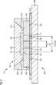
Ein optoelektronisches Bauelement umfasst einen optoelektronischen Halbleiterchip mit einem ersten elektrischen Kontakt und einem zweiten elektrischen Kontakt, einen ersten Leiterrahmenabschnitt, der eine erste Chipkontaktfläche und eine der ersten Chipkontaktfläche gegenüberliegende erste Lötkontaktfläche aufweist, und einen zweiten Leiterrahmenabschnitt, der eine zweite Chipkontaktfläche und eine der zweiten Chipkontaktfläche gegenüberliegende zweite Lötkontaktfläche aufweist. Dabei ist der erste elektrische Kontakt elektrisch leitend mit der ersten Chipkontaktfläche und der zweite elektrische Kontakt elektrisch leitend mit der zweiten Chipkontaktfläche verbunden. Der erste Leiterrahmenabschnitt und der zweite Leiterrahmenabschnitt sind derart in ein Gehäuse eingebettet, dass zumindest Teile der ersten Lötkontaktfläche und der zweiten Lötkontaktfläche an einer Unterseite des Gehäuses zugänglich sind. An der Unterseite des Gehäuses ist ein Lötstoppelement angeordnet, das sich zwischen der ersten Lötkontaktfläche und der zweiten Lötkontaktfläche erstreckt. Vorteilhafterweise bewirkt das an der Unterseite des Gehäuses dieses optoelektronischen Bauelements angeordnete Lötstoppelement eine elektrische Isolation zwischen der ersten Lötkontaktfläche des ersten Leiterrahmenabschnitts und der zweiten Lötkontaktfläche des zweiten Leiterrahmenabschnitts. Das an der Unterseite des Gehäuses angeordnete Lötstoppelement verhindert außerdem insbesondere ein Verfließen von Lot zwischen der ersten Lötkontaktfläche und der zweiten Lötkontaktfläche des optoelektronischen Bauelements. Dadurch wird ein unerwünschter Kurzschluss zwischen der ersten Lötkontaktfläche und der zweiten Lötkontaktfläche des optoelektronischen Bauelements vorteilhafterweise verhindert.An optoelectronic component comprises an optoelectronic semiconductor chip with a first electrical contact and a second electrical contact, a first leadframe section having a first chip contact surface and a first solder contact pad opposite the first chip contact surface, and a second leadframe section having a second chip contact surface and one of the second chip contact surface Having opposite second solder pad. In this case, the first electrical contact is electrically conductively connected to the first chip contact surface and the second electrical contact is electrically conductively connected to the second chip contact surface. The first lead frame portion and the second lead frame portion are embedded in a housing such that at least portions of the first solder pad and the second solder pad are accessible at an underside of the housing. At the bottom of the housing, a solder stop element is arranged which extends between the first solder pad and the second solder pad. Advantageously, the solder stop element arranged on the underside of the housing of this optoelectronic component effects an electrical insulation between the first solder contact area of the first conductor frame section and the second solder contact area of the second lead frame section. The solder stop element disposed on the underside of the housing also prevents in particular a flow of solder between the first solder pad and the second solder pad of the optoelectronic device. As a result, an undesired short circuit between the first solder contact area and the second solder contact area of the optoelectronic component is advantageously prevented.
In einer Ausführungsform des optoelektronischen Bauelements weisen die erste Lötkontaktfläche und die zweite Lötkontaktfläche einen Abstand von weniger als 200 µm auf. Vorteilhafterweise kann das optoelektronische Bauelement dadurch sehr kompakt ausgebildet sein. Insbesondere kann auch der optoelektronische Halbleiterchip des optoelektronischen Bauelements sehr kompakt ausgebildet sein, da der optoelektronische Halbleiterchip lediglich einen Abstand von weniger als 200 µm zwischen der ersten Lötkontaktfläche des ersten Leiterrahmenabschnitts und der zweiten Lötkontaktfläche des zweiten Leiterrahmenabschnitts des optoelektronischen Bauelements überbrücken muss.In one embodiment of the optoelectronic component, the first solder contact area and the second solder contact area have a spacing of less than 200 μm. Advantageously, the optoelectronic component can thereby be made very compact. In particular, the optoelectronic semiconductor chip of the optoelectronic component can also be made very compact, since the optoelectronic semiconductor chip only has to bridge a distance of less than 200 μm between the first solder contact area of the first conductor frame section and the second solder contact area of the second lead frame section of the optoelectronic component.
In einer Ausführungsform des optoelektronischen Bauelements bedeckt das Lötstoppelement die erste Lötkontaktfläche und/oder die zweite Lötkontaktfläche teilweise. Vorteilhafterweise vergrößert das Lötstoppelement dadurch einen wirksamen Abstand zwischen der ersten Lötkontaktfläche und der zweiten Lötkontaktfläche, wodurch ein unerwünschter Kurzschluss zwischen der ersten Lötkontaktfläche und der zweiten Lötkontaktfläche des optoelektronischen Bauelements vorteilhafterweise trotz eines geringen Abstands zwischen der ersten Lötkontaktfläche und der zweiten Lötkontaktfläche verhindert werden kann.In one embodiment of the optoelectronic component, the solder stop element partially covers the first solder contact area and / or the second solder contact area. Advantageously, the solder stop element thereby increases an effective distance between the first solder pad and the second solder pad, whereby an undesirable short circuit between the first solder pad and the second solder pad of the optoelectronic device advantageously despite a small distance between the first solder pad and the second solder pad can be prevented.
In einer Ausführungsform des optoelektronischen Bauelements weist das Lötstoppelement eine Kantenlänge von mindestens 200 µm auf. Vorteilhafterweise kann dadurch weitgehend sichergestellt werden, dass es während einer Oberflächenmontage des optoelektronischen Bauelements nicht zu einem Verfließen von Lot zwischen der ersten Lötkontaktfläche und der zweiten Lötkontaktfläche und dadurch zu einem elektrischen Kurzschluss zwischen der ersten Lötkontaktfläche und der zweiten Lötkontaktfläche des optoelektronischen Bauelements kommt. In one embodiment of the optoelectronic component, the solder stop element has an edge length of at least 200 μm. Advantageously, this can largely ensure that during a surface mounting of the optoelectronic component there is no flow of solder between the first solder contact area and the second solder contact area and thereby an electrical short circuit between the first solder contact area and the second solder contact area of the optoelectronic component.
In einer Ausführungsform des optoelektronischen Bauelements schließen die erste Lötkontaktfläche und die zweite Lötkontaktfläche bündig mit der Unterseite des Gehäuses ab. Vorteilhafterweise eignet sich das optoelektronische Bauelement dadurch besonders gut für eine Oberflächenmontage.In one embodiment of the optoelectronic component, the first solder contact area and the second solder contact area terminate flush with the underside of the housing. Advantageously, the optoelectronic component is thereby particularly well suited for surface mounting.
In einer Ausführungsform des optoelektronischen Bauelements weist das Gehäuse an einer der Unterseite gegenüberliegenden Oberseite eine Kavität auf. Dabei sind zumindest Teile der ersten Chipkontaktfläche und der zweiten Chipkontaktfläche in der Kavität zugänglich. Der optoelektronische Halbleiterchip ist in der Kavität angeordnet. Vorteilhafterweise kann die Kavität des Gehäuses des optoelektronischen Bauelements einem mechanischen Schutz des optoelektronischen Halbleiterchips dienen. Außerdem kann die Kavität als optischer Reflektor für durch den optoelektronischen Halbleiterchip des optoelektronischen Bauelements emittierte elektromagnetische Strahlung dienen. Die Kavität kann auch zur Aufnahme von den optoelektronischen Halbleiterchip einbettendem Vergussmaterial dienen.In one embodiment of the optoelectronic component, the housing has a cavity on an upper side opposite the underside. In this case, at least parts of the first chip contact area and the second chip contact area in the cavity are accessible. The optoelectronic semiconductor chip is arranged in the cavity. Advantageously, the cavity of the housing of the optoelectronic component can serve for a mechanical protection of the optoelectronic semiconductor chip. In addition, the cavity can serve as an optical reflector for electromagnetic radiation emitted by the optoelectronic semiconductor chip of the optoelectronic component. The cavity can also serve for receiving the optoelectronic semiconductor chip embedding potting material.
In einer Ausführungsform des optoelektronischen Bauelements ist in der Kavität ein Vergussmaterial angeordnet. Vorteilhafterweise kann das Vergussmaterial einen Schutz des optoelektronischen Halbleiterchips vor einer Beschädigung durch äußere mechanische Einwirkungen bewirken. Das Vergussmaterial kann auch eingebettete Konverterpartikel aufweisen, die dazu vorgesehen sind, eine Wellenlänge einer durch den optoelektronischen Halbleiterchip emittierten elektromagnetischen Strahlung zu konvertieren.In one embodiment of the optoelectronic component, a potting material is arranged in the cavity. Advantageously, the potting material can protect the optoelectronic semiconductor chip from being damaged by external mechanical effects. The potting material may also comprise embedded converter particles which are intended to convert a wavelength of an electromagnetic radiation emitted by the optoelectronic semiconductor chip.
In einer Ausführungsform des optoelektronischen Bauelements sind der erste elektrische Kontakt und der zweite elektrische Kontakt auf einer gemeinsamen Oberfläche des optoelektronischen Halbleiterchips angeordnet. Der optoelektronische Halbleiterchip kann dabei beispielsweise als Flipchip ausgebildet sein. Vorteilhafterweise ergibt sich dadurch eine besonders kompakte Ausführung des optoelektronischen Halbleiterchips und des optoelektronischen Bauelements.In one embodiment of the optoelectronic component, the first electrical contact and the second electrical contact are arranged on a common surface of the optoelectronic semiconductor chip. The optoelectronic semiconductor chip can be designed, for example, as a flip chip. Advantageously, this results in a particularly compact design of the optoelectronic semiconductor chip and the optoelectronic component.
In einer Ausführungsform des optoelektronischen Bauelements ist der optoelektronische Halbleiterchip als volumenemittierender Saphir-Flipchip ausgebildet. Vorteilhafterweise kann der optoelektronische Halbleiterchip dadurch mit besonders kompakten Abmessungen ausgebildet sein.In one embodiment of the optoelectronic component, the optoelectronic semiconductor chip is designed as a volume-emitting sapphire flip-chip. Advantageously, the optoelectronic semiconductor chip can thereby be formed with particularly compact dimensions.
In einer Ausführungsform des optoelektronischen Bauelements ist die die elektrischen Kontakte aufweisende Oberfläche des optoelektronischen Halbleiterchips den Chipkontaktflächen zugewandt. Dadurch können direkte elektrisch leitende Verbindungen zwischen den elektrischen Kontakten des optoelektronischen Halbleiterchips und den Chipkontaktflächen der Leiterrahmenabschnitte des optoelektronischen Bauelements bestehen. Beispielsweise können die elektrischen Kontakte über Lötverbindungen mit den Chipkontaktflächen verbunden sein. Eine Verwendung von Bonddrähten ist vorteilhafterweise nicht erforderlich.In one embodiment of the optoelectronic component, the surface of the optoelectronic semiconductor chip having the electrical contacts faces the chip contact surfaces. As a result, there can be direct electrically conductive connections between the electrical contacts of the optoelectronic semiconductor chip and the chip contact areas of the leadframe sections of the optoelectronic component. For example, the electrical contacts may be connected via solder connections to the chip contact surfaces. A use of bonding wires is advantageously not required.
Ein Verfahren zum Herstellen eines optoelektronischen Bauelements umfasst Schritte zum Einbetten eines ersten Leiterrahmenabschnitts mit einer ersten Lötkontaktfläche und eines zweiten Leiterrahmenabschnitts mit einer zweiten Lötkontaktfläche in ein Gehäuse derart, dass zumindest Teile der ersten Lötkontaktfläche und der zweiten Lötkontaktfläche an einer Unterseite des Gehäuses zugänglich bleiben, und zum Anordnen eines Lötstoppelements an der Unterseite des Gehäuses zwischen der ersten Lötkontaktfläche und der zweiten Lötkontaktfläche. Vorteilhafterweise ermöglicht dieses Verfahren eine Herstellung eines optoelektronischen Bauelements mit äußerst kompakten Abmessungen. Dabei wird durch das an der Unterseite des Gehäuses angeordnete Lötstoppelement trotz der möglichen kompakten Abmessungen des optoelektronischen Bauelements sichergestellt, dass es während einer Montage des optoelektronischen Bauelements nicht zu einem Verfließen von Lot zwischen der ersten Lötkontaktfläche und der zweiten Lötkontaktfläche und einem sich daraus ergebenden elektrischen Kurzschluss zwischen der ersten Lötkontaktfläche und der zweiten Lötkontaktfläche kommt.A method of fabricating an optoelectronic device includes steps of embedding a first leadframe portion having a first soldering pad and a second leadframe portion having a second soldering pad in a housing such that at least portions of the first soldering pad and the second soldering pad are accessible at a bottom surface of the housing; for placing a solder stop at the bottom of the housing between the first solder pad and the second solder pad. Advantageously, this method makes it possible to produce an optoelectronic component with extremely compact dimensions. In spite of the possible compact dimensions of the optoelectronic component, the solder resistive element arranged on the underside of the housing does not lead to a flow of solder between the first solder contact area and the second solder contact area during a mounting of the optoelectronic component and an electrical short circuit resulting therefrom comes between the first solder pad and the second solder pad.
In einer Ausführungsform des Verfahrens umfasst dieses einen weiteren Schritt zum Anordnen eines optoelektronischen Halbleiterchips in einer Kavität an einer der Unterseite gegenüberliegenden Oberseite des Gehäuses. Vorteilhafterweise kann der optoelektronische Halbleiterchip mit äußerst kompakten äußeren Abmessungen ausgebildet sein.In one embodiment of the method, this comprises a further step for arranging an optoelectronic semiconductor chip in a cavity on an upper side of the housing opposite the underside. Advantageously, the optoelectronic semiconductor chip can be formed with extremely compact external dimensions.
In einer Ausführungsform des Verfahrens wird das Lötstoppelement als Lötstopplack auf die Unterseite des Gehäuses aufgebracht. Vorteilhafterweise ist das Verfahren dadurch kostengünstig durchführbar und eignet sich für eine Massenproduktion.In one embodiment of the method, the solder stop element is applied as a solder resist to the underside of the housing. Advantageously, the method is thereby inexpensive to carry out and is suitable for mass production.
In einer Ausführungsform des Verfahrens erfolgt das Anordnen des Lötstoppelements mittels einer Maske. Vorteilhafterweise ist das Verfahren dadurch einfach und kostengünstig durchführbar und eignet sich für eine Massenproduktion.In one embodiment of the method, the solder stop element is arranged by means of a mask. Advantageously, the method is thereby simple and cost-effective and suitable for mass production.
In einer Ausführungsform des Verfahrens erfolgt das Einbetten des ersten Leiterrahmenabschnitts und des zweiten Leiterrahmenabschnitts in das Gehäuse durch ein Spritzgussverfahren. Vorteilhafterweise ist das Verfahren dadurch einfach und kostengünstig durchführbar und eignet sich für eine Massenproduktion.In one embodiment of the method, the embedding of the first leadframe section and the second leadframe section in the housing takes place by an injection molding process. Advantageously, the method is thereby simple and inexpensive to carry out and is suitable for mass production.
Die oben beschriebenen Eigenschaften, Merkmale und Vorteile dieser Erfindung sowie die Art und Weise, wie diese erreicht werden, werden klarer und deutlicher verständlich im Zusammenhang mit der folgenden Beschreibung der Ausführungsbeispiele, die im Zusammenhang mit den Zeichnungen näher erläutert werden. Dabei zeigen in jeweils schematisierter DarstellungThe above-described characteristics, features, and advantages of this invention, as well as the manner in which they will be achieved, will become clearer and more clearly understood in connection with the following description of the embodiments, which will be described in detail in conjunction with the drawings. In each case show in a schematic representation
Das optoelektronische Bauelement
Der optoelektronische Halbleiterchip
Der optoelektronische Halbleiterchip
Das optoelektronische Bauelement
Das Gehäuse
In das Gehäuse
Der erste Leiterrahmenabschnitt
Teile der ersten Chipkontaktfläche
Teile der ersten Lötkontaktfläche
Der optoelektronische Halbleiterchip
Der erste elektrische Kontakt
Die erste Chipkontaktfläche
Durch den geringen Abstand
An der Unterseite
Das Lötstoppelement
In der Kavität
Das Vergussmaterial
Das an der Unterseite
Die Leiterplatte
Das optoelektronische Bauelement
Die erste Lötkontaktfläche
Durch den Abstand
Die Erfindung wurde anhand der bevorzugten Ausführungsbeispiele näher illustriert und beschrieben. Dennoch ist die Erfindung nicht auf die offenbarten Beispiele eingeschränkt. Vielmehr können hieraus andere Variationen vom Fachmann abgeleitet werden, ohne den Schutzumfang der Erfindung zu verlassen.The invention has been further illustrated and described with reference to the preferred embodiments. However, the invention is not limited to the disclosed examples. Rather, other variations may be deduced therefrom by those skilled in the art without departing from the scope of the invention.
BezugszeichenlisteLIST OF REFERENCE NUMBERS
- 1010
- optoelektronisches Bauelementoptoelectronic component
- 100100
- optoelektronischer Halbleiterchipoptoelectronic semiconductor chip
- 101101
- Emissionsseiteemission side
- 102102
- KontaktseiteContact
- 110110
- erster elektrischen Kontaktfirst electrical contact
- 120120
- zweiter elektrischen Kontaktsecond electrical contact
- 200200
- erster Leiterrahmenabschnittfirst ladder frame section
- 210210
- erste Chipkontaktflächefirst chip contact surface
- 220220
- erste Lötkontaktflächefirst solder contact surface
- 250250
- Abstanddistance
- 300300
- zweiter Leiterrahmenabschnittsecond ladder frame section
- 310310
- zweite Chipkontaktflächesecond chip contact surface
- 320320
- zweite Lötkontaktflächesecond solder contact surface
- 400400
- Gehäusecasing
- 401401
- Oberseitetop
- 402402
- Unterseitebottom
- 410410
- Kavitätcavity
- 420420
- Vergussmaterialgrout
- 500500
- LötstoppelementLötstoppelement
- 510510
- Kantenlängeedge length
- 600600
- Leiterplattecircuit board
- 610610
- erste Lötkontaktflächefirst solder contact surface
- 620620
- zweite Lötkontaktflächesecond solder contact surface
- 630630
- Abstanddistance
Claims (15)
Translated fromGermanPriority Applications (4)
| Application Number | Priority Date | Filing Date | Title |
|---|---|---|---|
| DE102014101556.8ADE102014101556A1 (en) | 2014-02-07 | 2014-02-07 | Optoelectronic component and method for its production |
| PCT/EP2015/052176WO2015117947A1 (en) | 2014-02-07 | 2015-02-03 | Optoelectronic component and method for the production thereof |
| CN201580007512.3ACN105960715B (en) | 2014-02-07 | 2015-02-03 | Optoelectronic component and production method thereof |
| US15/649,987US10411157B2 (en) | 2014-02-07 | 2017-07-14 | Optoelectronic component and method for the production thereof |
Applications Claiming Priority (1)
| Application Number | Priority Date | Filing Date | Title |
|---|---|---|---|
| DE102014101556.8ADE102014101556A1 (en) | 2014-02-07 | 2014-02-07 | Optoelectronic component and method for its production |
Publications (1)
| Publication Number | Publication Date |
|---|---|
| DE102014101556A1true DE102014101556A1 (en) | 2015-08-13 |
Family
ID=52440692
Family Applications (1)
| Application Number | Title | Priority Date | Filing Date |
|---|---|---|---|
| DE102014101556.8APendingDE102014101556A1 (en) | 2014-02-07 | 2014-02-07 | Optoelectronic component and method for its production |
Country Status (4)
| Country | Link |
|---|---|
| US (1) | US10411157B2 (en) |
| CN (1) | CN105960715B (en) |
| DE (1) | DE102014101556A1 (en) |
| WO (1) | WO2015117947A1 (en) |
Cited By (1)
| Publication number | Priority date | Publication date | Assignee | Title |
|---|---|---|---|---|
| WO2017129698A1 (en)* | 2016-01-28 | 2017-08-03 | Osram Opto Semiconductors Gmbh | Production of a multi-chip component |
Citations (3)
| Publication number | Priority date | Publication date | Assignee | Title |
|---|---|---|---|---|
| US20110309404A1 (en)* | 2010-08-09 | 2011-12-22 | Lg Innotek Co., Ltd. | Light emitting device and lighting system having the same |
| US20120193661A1 (en)* | 2007-11-14 | 2012-08-02 | Cree, Inc. | Gap engineering for flip-chip mounted horizontal leds |
| US20130001633A1 (en)* | 2011-06-29 | 2013-01-03 | Hitachi Cable, Ltd. | Light-emitting element mounting substrate and led package |
Family Cites Families (8)
| Publication number | Priority date | Publication date | Assignee | Title |
|---|---|---|---|---|
| US7459345B2 (en)* | 2004-10-20 | 2008-12-02 | Mutual-Pak Technology Co., Ltd. | Packaging method for an electronic element |
| US9502624B2 (en)* | 2006-05-18 | 2016-11-22 | Nichia Corporation | Resin molding, surface mounted light emitting apparatus and methods for manufacturing the same |
| JP5310672B2 (en)* | 2009-10-15 | 2013-10-09 | 日亜化学工業株式会社 | Light emitting device and manufacturing method thereof |
| JP5756803B2 (en)* | 2010-07-23 | 2015-07-29 | シャープ株式会社 | Light emitting device and manufacturing method thereof |
| CN102569595A (en)* | 2010-12-29 | 2012-07-11 | 展晶科技(深圳)有限公司 | Packaging structure of light-emitting diode |
| CN102881812B (en)* | 2011-07-15 | 2015-03-25 | 赛恩倍吉科技顾问(深圳)有限公司 | Manufacturing method for Light emitting diode packaging structure |
| CN104103734B (en)* | 2013-04-02 | 2017-03-01 | 展晶科技(深圳)有限公司 | Package structure for LED |
| CN103247743B (en)* | 2013-05-24 | 2016-04-20 | 安徽三安光电有限公司 | Surface-mounted light-emitting device and manufacturing method thereof |
- 2014
- 2014-02-07DEDE102014101556.8Apatent/DE102014101556A1/enactivePending
- 2015
- 2015-02-03WOPCT/EP2015/052176patent/WO2015117947A1/enactiveApplication Filing
- 2015-02-03CNCN201580007512.3Apatent/CN105960715B/enactiveActive
- 2017
- 2017-07-14USUS15/649,987patent/US10411157B2/enactiveActive
Patent Citations (3)
| Publication number | Priority date | Publication date | Assignee | Title |
|---|---|---|---|---|
| US20120193661A1 (en)* | 2007-11-14 | 2012-08-02 | Cree, Inc. | Gap engineering for flip-chip mounted horizontal leds |
| US20110309404A1 (en)* | 2010-08-09 | 2011-12-22 | Lg Innotek Co., Ltd. | Light emitting device and lighting system having the same |
| US20130001633A1 (en)* | 2011-06-29 | 2013-01-03 | Hitachi Cable, Ltd. | Light-emitting element mounting substrate and led package |
Cited By (4)
| Publication number | Priority date | Publication date | Assignee | Title |
|---|---|---|---|---|
| WO2017129698A1 (en)* | 2016-01-28 | 2017-08-03 | Osram Opto Semiconductors Gmbh | Production of a multi-chip component |
| DE102016101526A1 (en)* | 2016-01-28 | 2017-08-03 | Osram Opto Semiconductors Gmbh | Production of a multi-chip component |
| CN108496250A (en)* | 2016-01-28 | 2018-09-04 | 奥斯兰姆奥普托半导体有限责任公司 | The manufacture of multi-chip module |
| US10886145B2 (en) | 2016-01-28 | 2021-01-05 | Osram Oled Gmbh | Production of a multi-chip component |
Also Published As
| Publication number | Publication date |
|---|---|
| CN105960715B (en) | 2018-12-28 |
| CN105960715A (en) | 2016-09-21 |
| US10411157B2 (en) | 2019-09-10 |
| US20170317233A1 (en) | 2017-11-02 |
| WO2015117947A1 (en) | 2015-08-13 |
Similar Documents
| Publication | Publication Date | Title |
|---|---|---|
| DE102016119002B4 (en) | OPTOELECTRONIC DEVICE AND METHOD FOR MANUFACTURING OPTOELECTRONIC DEVICE | |
| DE102010023815A1 (en) | Surface-mountable optoelectronic component and method for producing a surface-mountable optoelectronic component | |
| DE102007001706A1 (en) | Housing for optoelectronic component and arrangement of an optoelectronic component in a housing | |
| EP1717871B1 (en) | Optoelectronic surface-mountable component | |
| WO2009132618A1 (en) | Surface-mounted led module and method for producing a surface-mounted led module | |
| EP3360167A1 (en) | Optoelectronic component having a lead frame having a stiffening structure | |
| WO2022033926A1 (en) | Optoelectronic semiconductor component and production method | |
| DE102013215650A1 (en) | Optoelectronic component and method for its production | |
| DE102013219780A1 (en) | Power semiconductor module and method for producing a power semiconductor module | |
| DE102012107668A1 (en) | component assembly | |
| DE102013214730B4 (en) | Electronic circuit and manufacturing method therefor | |
| DE102013207111B4 (en) | Optoelectronic component | |
| EP3229269B1 (en) | Led module in chip on board technology | |
| DE102017210901A1 (en) | Semiconductor device and method of manufacturing the same | |
| DE102014101556A1 (en) | Optoelectronic component and method for its production | |
| DE102013221429A1 (en) | Optoelectronic component and method for its production | |
| DE112014005124B4 (en) | optoelectronic component | |
| DE102014101557A1 (en) | Optoelectronic component and method for its production | |
| DE102014116080A1 (en) | Optoelectronic component and method for its production | |
| DE10319782B4 (en) | Optoelectronic semiconductor component with a chip carrier element | |
| DE102010033868A1 (en) | Chip carrier, electronic component with chip carrier and method for producing a chip carrier | |
| DE102013211853A1 (en) | Optoelectronic component and method for its production | |
| DE102011011861A1 (en) | Semiconductor chip package assembly and manufacturing method | |
| DE102014102259A1 (en) | Optoelectronic component and method for its production | |
| DE102016107249A1 (en) | Circuit board with recess for electrical component |
Legal Events
| Date | Code | Title | Description |
|---|---|---|---|
| R163 | Identified publications notified | ||
| R012 | Request for examination validly filed | ||
| R016 | Response to examination communication | ||
| R079 | Amendment of ipc main class | Free format text:PREVIOUS MAIN CLASS: H01L0033620000 Ipc:H10H0020857000 |