DE102013204763A1 - Micromechanical sensor device and corresponding manufacturing method - Google Patents
Micromechanical sensor device and corresponding manufacturing methodDownload PDFInfo
- Publication number
- DE102013204763A1 DE102013204763A1DE102013204763.0ADE102013204763ADE102013204763A1DE 102013204763 A1DE102013204763 A1DE 102013204763A1DE 102013204763 ADE102013204763 ADE 102013204763ADE 102013204763 A1DE102013204763 A1DE 102013204763A1
- Authority
- DE
- Germany
- Prior art keywords
- layer
- sensor
- sensor elements
- contact
- substrate
- Prior art date
- Legal status (The legal status is an assumption and is not a legal conclusion. Google has not performed a legal analysis and makes no representation as to the accuracy of the status listed.)
- Withdrawn
Links
Images


Classifications
- H—ELECTRICITY
- H10—SEMICONDUCTOR DEVICES; ELECTRIC SOLID-STATE DEVICES NOT OTHERWISE PROVIDED FOR
- H10N—ELECTRIC SOLID-STATE DEVICES NOT OTHERWISE PROVIDED FOR
- H10N15/00—Thermoelectric devices without a junction of dissimilar materials; Thermomagnetic devices, e.g. using the Nernst-Ettingshausen effect
- H10N15/10—Thermoelectric devices using thermal change of the dielectric constant, e.g. working above and below the Curie point
- G—PHYSICS
- G01—MEASURING; TESTING
- G01J—MEASUREMENT OF INTENSITY, VELOCITY, SPECTRAL CONTENT, POLARISATION, PHASE OR PULSE CHARACTERISTICS OF INFRARED, VISIBLE OR ULTRAVIOLET LIGHT; COLORIMETRY; RADIATION PYROMETRY
- G01J5/00—Radiation pyrometry, e.g. infrared or optical thermometry
- G01J5/02—Constructional details
- G01J5/04—Casings
- G01J5/041—Mountings in enclosures or in a particular environment
- G01J5/045—Sealings; Vacuum enclosures; Encapsulated packages; Wafer bonding structures; Getter arrangements
- G—PHYSICS
- G01—MEASURING; TESTING
- G01J—MEASUREMENT OF INTENSITY, VELOCITY, SPECTRAL CONTENT, POLARISATION, PHASE OR PULSE CHARACTERISTICS OF INFRARED, VISIBLE OR ULTRAVIOLET LIGHT; COLORIMETRY; RADIATION PYROMETRY
- G01J5/00—Radiation pyrometry, e.g. infrared or optical thermometry
- G01J5/02—Constructional details
- G01J5/0225—Shape of the cavity itself or of elements contained in or suspended over the cavity
- G01J5/024—Special manufacturing steps or sacrificial layers or layer structures
- G—PHYSICS
- G01—MEASURING; TESTING
- G01J—MEASUREMENT OF INTENSITY, VELOCITY, SPECTRAL CONTENT, POLARISATION, PHASE OR PULSE CHARACTERISTICS OF INFRARED, VISIBLE OR ULTRAVIOLET LIGHT; COLORIMETRY; RADIATION PYROMETRY
- G01J5/00—Radiation pyrometry, e.g. infrared or optical thermometry
- G01J5/02—Constructional details
- G01J5/08—Optical arrangements
- G01J5/0853—Optical arrangements having infrared absorbers other than the usual absorber layers deposited on infrared detectors like bolometers, wherein the heat propagation between the absorber and the detecting element occurs within a solid
- G—PHYSICS
- G01—MEASURING; TESTING
- G01J—MEASUREMENT OF INTENSITY, VELOCITY, SPECTRAL CONTENT, POLARISATION, PHASE OR PULSE CHARACTERISTICS OF INFRARED, VISIBLE OR ULTRAVIOLET LIGHT; COLORIMETRY; RADIATION PYROMETRY
- G01J5/00—Radiation pyrometry, e.g. infrared or optical thermometry
- G01J5/10—Radiation pyrometry, e.g. infrared or optical thermometry using electric radiation detectors
- G01J5/34—Radiation pyrometry, e.g. infrared or optical thermometry using electric radiation detectors using capacitors, e.g. pyroelectric capacitors
- H—ELECTRICITY
- H10—SEMICONDUCTOR DEVICES; ELECTRIC SOLID-STATE DEVICES NOT OTHERWISE PROVIDED FOR
- H10F—INORGANIC SEMICONDUCTOR DEVICES SENSITIVE TO INFRARED RADIATION, LIGHT, ELECTROMAGNETIC RADIATION OF SHORTER WAVELENGTH OR CORPUSCULAR RADIATION
- H10F30/00—Individual radiation-sensitive semiconductor devices in which radiation controls the flow of current through the devices, e.g. photodetectors
- H10F30/10—Individual radiation-sensitive semiconductor devices in which radiation controls the flow of current through the devices, e.g. photodetectors the devices being sensitive to infrared radiation, visible or ultraviolet radiation, and having no potential barriers, e.g. photoresistors
- H—ELECTRICITY
- H10—SEMICONDUCTOR DEVICES; ELECTRIC SOLID-STATE DEVICES NOT OTHERWISE PROVIDED FOR
- H10F—INORGANIC SEMICONDUCTOR DEVICES SENSITIVE TO INFRARED RADIATION, LIGHT, ELECTROMAGNETIC RADIATION OF SHORTER WAVELENGTH OR CORPUSCULAR RADIATION
- H10F71/00—Manufacture or treatment of devices covered by this subclass
- H—ELECTRICITY
- H10—SEMICONDUCTOR DEVICES; ELECTRIC SOLID-STATE DEVICES NOT OTHERWISE PROVIDED FOR
- H10F—INORGANIC SEMICONDUCTOR DEVICES SENSITIVE TO INFRARED RADIATION, LIGHT, ELECTROMAGNETIC RADIATION OF SHORTER WAVELENGTH OR CORPUSCULAR RADIATION
- H10F77/00—Constructional details of devices covered by this subclass
- H10F77/20—Electrodes
- G—PHYSICS
- G01—MEASURING; TESTING
- G01J—MEASUREMENT OF INTENSITY, VELOCITY, SPECTRAL CONTENT, POLARISATION, PHASE OR PULSE CHARACTERISTICS OF INFRARED, VISIBLE OR ULTRAVIOLET LIGHT; COLORIMETRY; RADIATION PYROMETRY
- G01J5/00—Radiation pyrometry, e.g. infrared or optical thermometry
- G01J5/10—Radiation pyrometry, e.g. infrared or optical thermometry using electric radiation detectors
- G01J5/34—Radiation pyrometry, e.g. infrared or optical thermometry using electric radiation detectors using capacitors, e.g. pyroelectric capacitors
- G01J2005/345—Arrays
Landscapes
- Physics & Mathematics (AREA)
- General Physics & Mathematics (AREA)
- Spectroscopy & Molecular Physics (AREA)
- Engineering & Computer Science (AREA)
- Manufacturing & Machinery (AREA)
- Power Engineering (AREA)
- Photometry And Measurement Of Optical Pulse Characteristics (AREA)
Abstract
Translated fromGermanDescription
Translated fromGermanDie Erfindung betrifft eine mikromechanische Sensorvorrichtung und ein entsprechendes Herstellungsverfahren.The invention relates to a micromechanical sensor device and a corresponding manufacturing method.
Stand der TechnikState of the art
Obwohl auch auf beliebige mikromechanische Bauelemente anwendbar, wird die vorliegende Erfindung und die ihr zugrundeliegende Problematik anhand von pyroelektrischen Infrarotsensoren auf Siliziumbasis erläutert.Although applicable to any micromechanical components, the present invention and its underlying problem is explained by means of pyroelectric infrared sensors based on silicon.
Pyroelektrische Infrarotsensoren sind aus der
Offenbarung der ErfindungDisclosure of the invention
Die Erfindung schafft eine mikromechanische Sensorvorrichtung nach Anspruch 1 und ein entsprechendes Herstellungsverfahren nach Anspruch 10.The invention provides a micromechanical sensor device according to
Bevorzugte Weiterbildungen sind Gegenstand der jeweiligen Unteransprüche.Preferred developments are the subject of the respective subclaims.
Vorteile der ErfindungAdvantages of the invention
Die der vorliegenden Erfindung zugrunde liegende Idee besteht darin, eine mikromechanische Sensorvorrichtung vorzusehen, welche Sensorelemente aufweist, die über Substratstützen mechanisch verankert und elektronisch kontaktiert sind und sich lateral über einen Hohlraum erstrecken.The idea on which the present invention is based is to provide a micromechanical sensor device which has sensor elements which are mechanically anchored and electronically contacted via substrate supports and extend laterally across a cavity.
Die vorliegende Erfindung schafft somit eine kostengünstige integrierte mikromechanische Sensorvorrichtung bzw. ein entsprechendes Herstellungsverfahren mit der Möglichkeit einer Verpackung auf Chipskala, wobei eine bevorzugte Verwendung eine Dünnfilm-Pyrometer-Kamera bzw. ein Dünnfilm-Pyrometer-Bewegungssensor ist.The present invention thus provides a low-cost integrated micromechanical sensor device and a corresponding manufacturing method with the possibility of packaging on a chip scale, a preferred use being a thin-film pyrometer camera or a thin-film pyrometer motion sensor.
Dieses erfindungsgemäße Herstellverfahren ermöglicht hohe Füllfaktoren der Sensorelemente. Die Baugröße kann durch die Chipskala-Verpackung verkleinert werden und ein mechanisches und/oder thermisches und/oder elektrisches Übersprechen der Sensorelemente untereinander kann durch die Trenngräben und den Hohlraum deutlich reduziert bzw. vollständig beseitigt werden.This manufacturing method according to the invention allows high filling factors of the sensor elements. The size can be reduced by the chip scale packaging and a mechanical and / or thermal and / or electrical crosstalk of the sensor elements with each other can be significantly reduced or completely eliminated by the separation trenches and the cavity.
Zum Opferschichtätzen des Substrats dienen die Trenngräben ebenfalls, können allerdings durch zusätzliche Opferschichtätzlöcher ergänzt werden. Der Rückkontakt sorgt für eine elektrische Anbindung aller Sensorelemente und dient gleichzeitig als Unterstützung des Pixels beim Bondvorgang. Hierbei ist es zweckmäßig, dass sich der Vorderseitenkontakt und der Rückseitenkontakt des jeweiligen Sensorelements möglichst vollständig überdecken. Der Rückseitenkontakt ist zweckmäßigerweise umlaufend mit einer Ätzstoppschicht, z.B. aus SiO2, vor dem Opferschichtätzmedium, z.B. einem Ätzgas, geschützt.For the sacrificial layer etching of the substrate, the separation trenches are also used, but can be supplemented by additional Opferschichtätzlöcher. The back contact ensures electrical connection of all sensor elements and at the same time serves as support for the pixel during the bonding process. In this case, it is expedient that the front-side contact and the rear-side contact of the respective sensor element cover as completely as possible. The rear-side contact is expediently protected circumferentially with an etching stop layer, for example of SiO2 , in front of the sacrificial layer etching medium, for example an etching gas.
Gemäß einer bevorzugten Weiterbildung weisen die Sensorelemente einen jeweiligen Vorderseitenkontakt auf, wobei die Vorderseitenkontakte auf einer der Rückseite gegenüberliegenden Seite, d. h. auf einer dem Substrat abgewandten Seite des Sensorelement, liegen. Dies ermöglicht eine raumsparende elektrische Anbindung.According to a preferred embodiment, the sensor elements have a respective front side contact, wherein the front side contacts on a side opposite the back, d. H. on a side facing away from the substrate of the sensor element lie. This allows a space-saving electrical connection.
Gemäß einer weiteren bevorzugten Weiterbildung weist das Substrat einen Randbereich mit einem Ringkontakt auf, der über eine entsprechende Randwandung auf die der Rückseite gegenüberliegenden Seite geführt ist und von den Sensorelementen durch die jeweiligen Trenngräben lateral beanstandet ist. So lässt sich das Substrat großflächig elektrisch anbinden und eine hermetisch dichte Verkappung schaffen.According to a further preferred development, the substrate has an edge region with a ring contact, which is guided over a corresponding edge wall on the opposite side of the back side and is laterally criticized by the sensor elements by the respective separation trenches. This allows the substrate to be electrically connected over a large area and to create a hermetically sealed cap.
Gemäß einer weiteren bevorzugten Weiterbildung sind die Sensorelemente infrarotsensitiv und weisen eine pyroelektrische Schicht auf, die zwischen einer ersten und zweiten Elektrodenschicht eingebettet ist. So lässt sich eine hochintegrierte Infrarotkamera bilden.According to a further preferred development, the sensor elements are infrared-sensitive and have a pyroelectric layer which is embedded between a first and second electrode layer. This makes it possible to form a highly integrated infrared camera.
Gemäß einer weiteren bevorzugten Weiterbildung weisen die Sensorelemente eine erste elektrisch isolierende Absorberschicht auf der ersten Elektrodenschicht und eine zweite elektrisch isolierende Absorberschicht auf der zweiten Elektrodenschicht auf. Dies schafft eine gute Lichtabsorption.According to a further preferred development, the sensor elements have a first electrically insulating absorber layer on the first electrode layer and a second electrically insulating absorber layer on the second electrode layer. This creates good light absorption.
Gemäß einer weiteren bevorzugten Weiterbildung sind die Säulen (S1, S2) von einer Ätzstoppschicht umgeben, welche vorzugsweise der ersten elektrisch isolierenden Absorberschicht entspricht. Dies ermöglicht eine Mehrfachfunktion der betreffenden Schicht und trägt zu einem gut kontrollierbaren Ätzprozess bei.According to a further preferred development, the columns (S1, S2) are surrounded by an etching stop layer, which preferably corresponds to the first electrically insulating absorber layer. This allows a multiple function of the layer in question and contributes to a well controllable etching process.
Gemäß einer weiteren bevorzugten Weiterbildung ist auf der der Rückseite gegenüberliegenden Seite eine Auswerteeinrichtung aufgebondet, welche den Ringkontakt und die Vorderseitenkontakte kontaktiert. So lässt sich die Auswerteeinrichtung platzsparend anschließen. According to a further preferred development, an evaluation device is bonded on the side opposite the rear side, which contacts the ring contact and the front side contacts. Thus, the evaluation can be connected to save space.
Gemäß einer weiteren bevorzugten Weiterbildung ist die Auswerteeinrichtung derart aufgebondet, dass sie den Hohlraum verschließt. So lässt sich im Hohlraum eine kontrollierte Atmosphäre bilden, z.B. ein Vakuum.According to a further preferred development, the evaluation device is bonded in such a way that it closes the cavity. Thus, a controlled atmosphere can be formed in the cavity, e.g. a vacuum.
Gemäß einer weiteren bevorzugten Weiterbildung weisen die Sensorelemente Ätzlöcher auf. So lässt dich der Opferschichtätzprozess beschleunigen und gut steuern.According to a further preferred development, the sensor elements have etching holes. This allows you to speed up and control the sacrificial layer etching process.
Kurze Beschreibung der ZeichnungenBrief description of the drawings
Weitere Merkmale und Vorteile der vorliegenden Erfindung werden nachfolgend anhand von Ausführungsformen mit Bezug auf die Figuren erläutert.Further features and advantages of the present invention will be explained below with reference to embodiments with reference to the figures.
Es zeigen:Show it:
Ausführungsformen der ErfindungEmbodiments of the invention
In den Figuren bezeichnen gleiche Bezugszeichen gleiche bzw. funktionsgleiche Elemente.In the figures, like reference numerals designate the same or functionally identical elements.
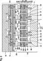
In
Auf der ersten Säule S1 und der zweiten Säule S2 ist ein jeweiliges Sensorelement P1 bzw. P2 in Form eines pyroelektrischen Pixelelements gebildet, wobei die Sensorelemente P1, P2 jeweils eine größere laterale Ausdehnung als die zugehörige Säule S1 bzw. S2 aufweisen und wobei seitlich der Säulen S1 bzw. S2 unterhalb der Sensorelemente P1 bzw. P2 ein Hohlraum H vorgesehen ist.On the first column S1 and the second column S2, a respective sensor element P1 or P2 is formed in the form of a pyroelectric pixel element, wherein the sensor elements P1, P2 each have a greater lateral extent than the associated column S1 or S2 and wherein laterally of the columns S1 or S2 below the sensor elements P1 and P2, a cavity H is provided.
Die Sensorelemente P1, P2 sind durch jeweilige Trenngräben G1, G2 lateral voneinander beabstandet und über die jeweils zugehörige Säule S1 bzw. S2 an ihrer jeweiligen Rückseite über die Säulen S1, S2 und Kontaktstöpsel V6, V7 elektrisch kontaktiert.The sensor elements P1, P2 are laterally spaced apart from one another by respective isolation trenches G1, G2 and electrically contacted via the respectively associated column S1 or S2 at their respective rear sides via the columns S1, S2 and contact plugs V6, V7.
Die Sensorelemente P1, P2 weisen eine untere elektrisch isolierende Schicht
Bei der pyroelektrischen Schicht PS handelt es sich beispielsweise um ein c-achsenorientiertes PZT (Bleizirkontitanat) oder BST (Barium-Strontium-Titanat). Bei den Elektrodenschichten E1, E2 handelt es sich beispielsweise um LNO (Lithiumniobat) oder SRO (Strontium-Ruthenium-Oxid).The pyroelectric layer PS is, for example, a c-axis-oriented PZT (lead zirconate titanate) or BST (barium strontium titanate). The electrode layers E1, E2 are, for example, LNO (lithium niobate) or SRO (strontium-ruthenium oxide).
Auf der Metallschicht
Das zweite Sensorelement P2 ist analog wie das erste Sensorelement P1 aufgebaut, wobei der in elektrischer Verbindung mit der Säule S2 und der ersten Elektrodenschicht E1 stehende Kontaktstöpsel mit Bezugszeichen V7 bezeichnet ist und wobei der mit der zweiten Elektrodenschicht E2 und der Metallschicht
Auf der Randwandung SB befindet sich ebenfalls die erste elektrisch isolierende Schicht
Auf der zweiten Elektrodenschicht E2 befindet sich im Randbereich RB ebenfalls die zweite elektrisch isolierende Schicht
Alle Bondkontakte BK1, BK2 und der Bondrahmenkontakt BR liegen somit gemeinsam auf der der Rückseite RS gegenüberliegenden Seite OS der Sensorvorrichtung und besitzen wegen eines identischen Schichtunterbaus dasselbe Niveau.All bond contacts BK1, BK2 and the bonding frame contact BR thus lie together on the opposite side of the back side RS OS of the sensor device and have the same level because of an identical layer structure.
Die Funktion der derart aufgebauten mikromechanischen Sensorrichtung, welche auch als Pixelsubstrat PS bezeichnet wird, besteht darin, dass Licht LI von der Rückseite RS her auf die Anordnung der Sensorelemente P1, P2 einfällt, dort in den Schichten
Bei pyroelektrischen Kristallen der pyroelektrischen Schicht PS handelt es sich um Ionenkristalle mit permanenter elektrischer Polarisation. Erwärmt man diese pyroelektrischen Kristalle oder kühlt sie ab, so laden sich gegenüberliegende Flächen entgegengesetzt elektrisch auf. Die resultierende Spannungsdifferenz kann an den entsprechenden Kristallkanten (Oberflächen) mit den Elektrodenschichten E1, E2 abgegriffen werden. Die Polarisation ist dabei proportional zur Temperaturänderung. Die vorhandenen Oberflächenladungen werden allerdings durch aus der Umgebung aufgenommene Ladungsträger kompensiert, z.B. freien Elektronen. Oberflächenladungen treten daher nur bei einer Änderung der Temperatur eines Pixels auf. Aufgrund dieser Eigenschaften lassen sich Bewegungen mit einer derartigen pyroelektrischen Kamera unter Verwendung von pyroelektrischen Pixelelementen bei dauerhaftem Lichteinfall sehr gut erfassen, da nur Bildelemente sichtbar werden, in denen sich die Infrarotstrahlung ändert. Für Standbilder dagegen muss der Lichteinfall mit einem Chopper moduliert werden.Pyroelectric crystals of the pyroelectric layer PS are ionic crystals with permanent electrical polarization. If these pyroelectric crystals are heated or cooled, opposing surfaces charge oppositely electrically. The resulting voltage difference can be tapped at the corresponding crystal edges (surfaces) with the electrode layers E1, E2. The polarization is proportional to the temperature change. However, the surface charges present are compensated by charge carriers taken from the environment, e.g. free electrons. Surface charges therefore occur only when the temperature of a pixel changes. Because of these properties, movements with such a pyroelectric camera using pyroelectric pixel elements can be detected very well with permanent incidence of light, since only picture elements in which the infrared radiation changes are visible. For still images, on the other hand, the incidence of light must be modulated with a chopper.
Das pyrometrische Pixelelement kann mit Absorberschichten für die jeweils interessierende Strahlung versehen sein, beispielsweise bei der vorliegenden Ausführungsform mit den Schichten
Somit kann die SiO2-Schicht eine Doppelfunktion als Ätzstoppschicht für die Stützen und Absorptionsschicht für die Sensorelemente übernehmen, wie weiter unten näher erläutert.Thus, the
Der Hohlraum H und die Trenngräben G1, G2 sorgen für eine gute thermische Isolation der Sensorelemente P1, P2 untereinander. Gemeinsam bestimmen der Vorderseiten- und Rückseitenkontakt der Sensorelemente P1, P2 somit die Wärmeableitung aus dem jeweiligen Sensorelement P1, P2. Ein geringer Querschnitt führt zu einem größeren Signalhub, ein größerer Querschnitt zu einer schnelleren Zeitkonstante des Pixels. Die genaue Dimensionierung hängt dafür von den speziellen gewünschten Funktionseigenschaften ab.The cavity H and the separation trenches G1, G2 provide for a good thermal insulation of the sensor elements P1, P2 with each other. Together, the front and rear contact of the sensor elements P1, P2 thus determine the heat dissipation from the respective sensor element P1, P2. A small cross section leads to a larger signal swing, a larger cross section to a faster time constant of the pixel. The exact dimensioning depends on the specific desired functional properties.
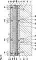
Das Substrat
Gemäß
Weiterhin weist das Schaltungssubstrat AS eine Bondverbindung BV an dessen dem Pixelsubstrat PS zugewandten Seite auf, der mit Bezugszeichen BV bezeichnet ist und über den Verdrahtungsbereich VL mit dem ’Schaltungsbereich SL elektrisch verbunden ist.Furthermore, the circuit substrate AS has a bonding connection BV on its side facing the pixel substrate PS, which is designated by reference BV and is electrically connected to the circuit region SL via the wiring region VL.
Die Bondverbindung wird vorzugsweise über Thermokompressionsbonden oder SLID(Solid-Liquid-Interdiffusion)-Bonden hergestellt.The bond connection is preferably produced via thermocompression bonding or SLID (solid-liquid interdiffusion) bonding.
Für das Bonden ist es von Vorteil, wenn die Bondrahmenkontakte BR, BR‘ und die Bondkontakte BK1, BK2 und BK1‘, BK2‘ unterschiedliche Größen aufweisen. Wenn die Größenunterschiede dabei die Justagetoleranzen der Ebenen zueinander berücksichtigen, wird der Bondprozess tolerant gegenüber Versetzen und es kommt zu keiner unerwünschten Verkippung der Sensorelemente. For the bonding, it is advantageous if the bonding frame contacts BR, BR 'and the bonding contacts BK1, BK2 and BK1', BK2 'have different sizes. If the differences in size take into account the alignment tolerances of the planes relative to one another, the bonding process is tolerant to displacement and there is no undesirable tilting of the sensor elements.
Sowohl bei der ersten als auch bei der zweiten Ausführungsform weisen der Bondrahmenkontakt BR‘ und die Bondkontakte BK1', BK2' des Auswertesubstrats AS eine größere laterale Ausdehnung auf als der Bondrahmenkontakt BR und die Bondkontakte BK1, BK2 des Pixelsubstrats PS.Both in the first and in the second embodiment, the bonding frame contact BR 'and the bonding contacts BK1', BK2 'of the evaluation substrate AS have a greater lateral extent than the bonding frame contact BR and the bonding contacts BK1, BK2 of the pixel substrate PS.
Bei der Ausführungsform gemäß
Dies geschieht ebenfalls über entsprechende Bondrahmenkontakte BR, BR' sowie Bondkontakte BK1, BK2 und BK1‘, BK2‘. Der Verdrahtungsbereich trägt bei dieser Ausführungsform Bezugszeichen VL' und weist zum Unterschied zum Verdrahtungsbereich VL der zweiten Ausführungsform eine Durchkontaktierung DK auf, sodass der Schaltungsbereich SL von der dem Pixelsubstrat PS gegenüberliegenden Seite des Auswertesubstrats AS' kontaktierbar ist.This also takes place via corresponding bonding frame contacts BR, BR 'as well as bond contacts BK1, BK2 and BK1', BK2 '. In this embodiment, the wiring region carries reference symbol VL 'and, unlike the wiring region VL of the second embodiment, has a via DK, so that the circuit region SL can be contacted by the side of the evaluation substrate AS' opposite the pixel substrate PS.
Wie in
In einem weiteren Prozessschritt werden die Ringgräben RG mit der ersten elektrisch isolierenden Schicht
In einem darauffolgenden Prozessschritt erfolgt ein Bilden der Kontaktstöpsel V6, V7, welche die erste und zweite Säule S1 bzw. S2 durch die erste elektrisch isolierende Schicht
Weiterhin mit Bezug auf
Auf der zweiten Elektrodenschicht E2 wird anschließend die zweite elektrisch isolierende Schicht
Weiter mit Bezug auf
In einem darauffolgenden Prozessschritt werden auf der Metallschicht
Wie in
Im Anschluss an den in
Somit ist gemäß
Die Herstellung der Verbindung mit dem Auswertesubstrat AS bzw. AS' gemäß der zweiten bzw. dritten Ausführungsform erfolgt dann vorzugsweise mittels eines bekannten Thermokompressionsbondschrittes oder SLID-Bondschrittes.The connection to the evaluation substrate AS or AS 'according to the second or third embodiment is then preferably carried out by means of a known thermocompression bonding step or SLID bonding step.
Obwohl die vorliegende Erfindung anhand bevorzugter Ausführungsbeispiele beschrieben wurde, ist sie darauf nicht beschränkt. Insbesondere sind die genannten Materialien und Topologien nur beispielhaft und nicht auf die erläuterten Beispiele beschränkt.Although the present invention has been described in terms of preferred embodiments, it is not limited thereto. In particular, the materials and topologies mentioned are only examples and not limited to the illustrated examples.
ZITATE ENTHALTEN IN DER BESCHREIBUNG QUOTES INCLUDE IN THE DESCRIPTION
Diese Liste der vom Anmelder aufgeführten Dokumente wurde automatisiert erzeugt und ist ausschließlich zur besseren Information des Lesers aufgenommen. Die Liste ist nicht Bestandteil der deutschen Patent- bzw. Gebrauchsmusteranmeldung. Das DPMA übernimmt keinerlei Haftung für etwaige Fehler oder Auslassungen.This list of the documents listed by the applicant has been generated automatically and is included solely for the better information of the reader. The list is not part of the German patent or utility model application. The DPMA assumes no liability for any errors or omissions.
Zitierte PatentliteraturCited patent literature
- US 5424544 A[0003]US 5424544 A[0003]
- US 6239433 B1[0003]US 6239433 B1[0003]
- WO 2010/119131 A1[0003]WO 2010/119131 A1[0003]
Claims (15)
Translated fromGermanPriority Applications (5)
| Application Number | Priority Date | Filing Date | Title |
|---|---|---|---|
| DE102013204763.0ADE102013204763A1 (en) | 2013-03-19 | 2013-03-19 | Micromechanical sensor device and corresponding manufacturing method |
| EP14709681.2AEP2976608A1 (en) | 2013-03-19 | 2014-03-13 | Micromechanical sensor device and corresponding production method |
| CN201480016877.8ACN105190265A (en) | 2013-03-19 | 2014-03-13 | Micromechanical sensor device and corresponding production method |
| US14/778,593US9780284B2 (en) | 2013-03-19 | 2014-03-13 | Micromechanical sensor device and corresponding production method |
| PCT/EP2014/054938WO2014146965A1 (en) | 2013-03-19 | 2014-03-13 | Micromechanical sensor device and corresponding production method |
Applications Claiming Priority (1)
| Application Number | Priority Date | Filing Date | Title |
|---|---|---|---|
| DE102013204763.0ADE102013204763A1 (en) | 2013-03-19 | 2013-03-19 | Micromechanical sensor device and corresponding manufacturing method |
Publications (1)
| Publication Number | Publication Date |
|---|---|
| DE102013204763A1true DE102013204763A1 (en) | 2014-09-25 |
Family
ID=50272636
Family Applications (1)
| Application Number | Title | Priority Date | Filing Date |
|---|---|---|---|
| DE102013204763.0AWithdrawnDE102013204763A1 (en) | 2013-03-19 | 2013-03-19 | Micromechanical sensor device and corresponding manufacturing method |
Country Status (5)
| Country | Link |
|---|---|
| US (1) | US9780284B2 (en) |
| EP (1) | EP2976608A1 (en) |
| CN (1) | CN105190265A (en) |
| DE (1) | DE102013204763A1 (en) |
| WO (1) | WO2014146965A1 (en) |
Cited By (2)
| Publication number | Priority date | Publication date | Assignee | Title |
|---|---|---|---|---|
| CN110627014A (en)* | 2019-09-19 | 2019-12-31 | 中国科学院上海微系统与信息技术研究所 | A method of making a suspended infrared thermal stack on a substrate |
| DE102015117059B4 (en) | 2015-10-07 | 2020-07-16 | Pyreos Ltd. | Absorption spectrometer |
Families Citing this family (3)
| Publication number | Priority date | Publication date | Assignee | Title |
|---|---|---|---|---|
| CN109956447A (en)* | 2017-12-25 | 2019-07-02 | 中芯国际集成电路制造(上海)有限公司 | A kind of MEMS device and preparation method, electronic device |
| FR3094789B1 (en)* | 2019-04-04 | 2021-05-28 | Elichens | Method of manufacturing a pyroelectric detector |
| CN113872544B (en)* | 2021-10-11 | 2024-12-17 | 中国科学院半导体研究所 | Preparation method of micromechanical resonator |
Citations (3)
| Publication number | Priority date | Publication date | Assignee | Title |
|---|---|---|---|---|
| US5424544A (en) | 1994-04-29 | 1995-06-13 | Texas Instruments Incorporated | Inter-pixel thermal isolation for hybrid thermal detectors |
| US6239433B1 (en) | 1997-01-14 | 2001-05-29 | Infrared Integrated Systems. Ltd. | Sensors using detector arrays |
| WO2010119131A1 (en) | 2009-04-17 | 2010-10-21 | Pyreos Ltd. | Infrared light sensor having a high signal voltage and a high signal/noise ratio |
Family Cites Families (8)
| Publication number | Priority date | Publication date | Assignee | Title |
|---|---|---|---|---|
| GB2206997A (en) | 1987-07-10 | 1989-01-18 | Philips Electronic Associated | Arrays of pyroelectric or ferroelectric infrared detector elements |
| GB2274543A (en) | 1993-01-21 | 1994-07-27 | Central Research Lab Ltd | Infrared detector |
| US5478242A (en)* | 1994-04-29 | 1995-12-26 | Texas Instruments Incorporated | Thermal isolation of hybrid thermal detectors through an anisotropic etch |
| US5577309A (en) | 1995-03-01 | 1996-11-26 | Texas Instruments Incorporated | Method for forming electrical contact to the optical coating of an infrared detector |
| DE10058864B4 (en)* | 2000-11-27 | 2009-06-25 | Pyreos Ltd. | Micromechanical structure for integrated sensor arrangements and method for producing a micromechanical structure |
| KR100538996B1 (en)* | 2003-06-19 | 2005-12-27 | 한국전자통신연구원 | Infrared ray sensor using silicon oxide film as a infrared ray absorption layer and method for fabricating the same |
| KR101375337B1 (en)* | 2005-07-22 | 2014-03-18 | 퀄컴 엠이엠에스 테크놀로지스, 인크. | Electomechanical devices having support structures and methods of fabricating the same |
| DE102007024902B8 (en) | 2007-05-29 | 2010-12-30 | Pyreos Ltd. | Device with membrane structure for the detection of thermal radiation, method for producing and using the device |
- 2013
- 2013-03-19DEDE102013204763.0Apatent/DE102013204763A1/ennot_activeWithdrawn
- 2014
- 2014-03-13USUS14/778,593patent/US9780284B2/ennot_activeExpired - Fee Related
- 2014-03-13EPEP14709681.2Apatent/EP2976608A1/ennot_activeWithdrawn
- 2014-03-13CNCN201480016877.8Apatent/CN105190265A/enactivePending
- 2014-03-13WOPCT/EP2014/054938patent/WO2014146965A1/enactiveApplication Filing
Patent Citations (3)
| Publication number | Priority date | Publication date | Assignee | Title |
|---|---|---|---|---|
| US5424544A (en) | 1994-04-29 | 1995-06-13 | Texas Instruments Incorporated | Inter-pixel thermal isolation for hybrid thermal detectors |
| US6239433B1 (en) | 1997-01-14 | 2001-05-29 | Infrared Integrated Systems. Ltd. | Sensors using detector arrays |
| WO2010119131A1 (en) | 2009-04-17 | 2010-10-21 | Pyreos Ltd. | Infrared light sensor having a high signal voltage and a high signal/noise ratio |
Cited By (3)
| Publication number | Priority date | Publication date | Assignee | Title |
|---|---|---|---|---|
| DE102015117059B4 (en) | 2015-10-07 | 2020-07-16 | Pyreos Ltd. | Absorption spectrometer |
| CN110627014A (en)* | 2019-09-19 | 2019-12-31 | 中国科学院上海微系统与信息技术研究所 | A method of making a suspended infrared thermal stack on a substrate |
| CN110627014B (en)* | 2019-09-19 | 2022-09-23 | 中国科学院上海微系统与信息技术研究所 | Method for manufacturing suspended infrared thermopile on substrate |
Also Published As
| Publication number | Publication date |
|---|---|
| US9780284B2 (en) | 2017-10-03 |
| EP2976608A1 (en) | 2016-01-27 |
| US20160056365A1 (en) | 2016-02-25 |
| CN105190265A (en) | 2015-12-23 |
| WO2014146965A1 (en) | 2014-09-25 |
Similar Documents
| Publication | Publication Date | Title |
|---|---|---|
| DE69937407T2 (en) | CAPTURE OF A DEVICE | |
| DE102013204763A1 (en) | Micromechanical sensor device and corresponding manufacturing method | |
| DE102010039057B4 (en) | sensor module | |
| DE202012013576U1 (en) | Solid-state imaging unit and electronic device | |
| DE602004001508T2 (en) | ELECTROCHROMIC DISPLAY DEVICE | |
| DE102015105451A1 (en) | Method and apparatus for forming backlit image sensors with embedded color filters | |
| DE102007012279B4 (en) | Image sensor, sensor array, sensor system and manufacturing process | |
| DE102010002463A1 (en) | Micromechanical pressure sensor element and method for its production | |
| KR102471593B1 (en) | Image sensor having vertical transfer gate and method for fabricating the same | |
| DE102016223203A1 (en) | Low-resistance wiring MEMS device and method of making the same | |
| DE102014200507A1 (en) | Micromechanical pressure sensor device and corresponding manufacturing method | |
| DE112017001139T5 (en) | MICRO DEVICE INTEGRATION IN SYSTEM SUBSTRATE | |
| DE102011102266A1 (en) | Assembly with a MEMS device and method of manufacture | |
| DE102018124442A1 (en) | Polarizers for image sensor devices | |
| DE102010029504A1 (en) | Device with a via and method for its production | |
| US20150048317A1 (en) | Solid state imaging device | |
| DE102016224977A1 (en) | Infrared heat detector and manufacturing process for infrared heat detector | |
| DE112022003621T5 (en) | Electronic device | |
| DE102008000261A1 (en) | Semiconductor device has cap electrical conductivity regions that function as draw-out electrical conductivity regions of cap substrate, are electrically connected to movable and fixed base semiconductor regions of base substrate | |
| DE102007024902A1 (en) | Device with membrane structure for detecting heat radiation, method for producing and using the device | |
| DE102008042382A1 (en) | Contact arrangement for producing a spaced, electrically conductive connection between microstructured components | |
| WO2008145354A1 (en) | Device having a sandwich structure for detecting thermal radiation, method of production and use of the device | |
| DE60223263T2 (en) | COLOR IMAGE SENSOR ON A TRANSPARENT SUBSTRATE AND METHOD FOR THE PRODUCTION THEREOF | |
| DE60126138T2 (en) | THREE-DIMENSIONAL ELECTROMAGNETIC RADIATION DETECTOR AND METHOD OF MANUFACTURING THEREOF | |
| DE102018122261A1 (en) | AN INTEGRATION PROCESS FOR WAFBERBENENPACKAGING |
Legal Events
| Date | Code | Title | Description |
|---|---|---|---|
| R119 | Application deemed withdrawn, or ip right lapsed, due to non-payment of renewal fee |