DE102013113648A1 - Power supply device and method for limiting an output current of a power supply device - Google Patents
Power supply device and method for limiting an output current of a power supply deviceDownload PDFInfo
- Publication number
- DE102013113648A1 DE102013113648A1DE102013113648.6ADE102013113648ADE102013113648A1DE 102013113648 A1DE102013113648 A1DE 102013113648A1DE 102013113648 ADE102013113648 ADE 102013113648ADE 102013113648 A1DE102013113648 A1DE 102013113648A1
- Authority
- DE
- Germany
- Prior art keywords
- current
- power supply
- supply device
- output
- voltage
- Prior art date
- Legal status (The legal status is an assumption and is not a legal conclusion. Google has not performed a legal analysis and makes no representation as to the accuracy of the status listed.)
- Pending
Links
- 238000000034methodMethods0.000titleclaimsabstractdescription12
- 239000003990capacitorSubstances0.000claimsdescription24
- 230000001419dependent effectEffects0.000claimsdescription10
- 238000007599dischargingMethods0.000claimsdescription9
- 230000010354integrationEffects0.000claimsdescription5
- 238000009499grossingMethods0.000description13
- 238000011156evaluationMethods0.000description6
- 238000010586diagramMethods0.000description4
- 230000001960triggered effectEffects0.000description3
- 230000008901benefitEffects0.000description2
- 238000001816coolingMethods0.000description2
- 238000012937correctionMethods0.000description2
- 238000009434installationMethods0.000description2
- 230000008929regenerationEffects0.000description2
- 238000011069regeneration methodMethods0.000description2
- 238000004804windingMethods0.000description2
- BUHVIAUBTBOHAG-FOYDDCNASA-N(2r,3r,4s,5r)-2-[6-[[2-(3,5-dimethoxyphenyl)-2-(2-methylphenyl)ethyl]amino]purin-9-yl]-5-(hydroxymethyl)oxolane-3,4-diolChemical compoundCOC1=CC(OC)=CC(C(CNC=2C=3N=CN(C=3N=CN=2)[C@H]2[C@@H]([C@H](O)[C@@H](CO)O2)O)C=2C(=CC=CC=2)C)=C1BUHVIAUBTBOHAG-FOYDDCNASA-N0.000description1
- 230000000712assemblyEffects0.000description1
- 238000000429assemblyMethods0.000description1
- 238000011161developmentMethods0.000description1
- 230000018109developmental processEffects0.000description1
- 238000005259measurementMethods0.000description1
- 238000013021overheatingMethods0.000description1
- 238000011144upstream manufacturingMethods0.000description1
Images

Classifications
- H—ELECTRICITY
- H02—GENERATION; CONVERSION OR DISTRIBUTION OF ELECTRIC POWER
- H02M—APPARATUS FOR CONVERSION BETWEEN AC AND AC, BETWEEN AC AND DC, OR BETWEEN DC AND DC, AND FOR USE WITH MAINS OR SIMILAR POWER SUPPLY SYSTEMS; CONVERSION OF DC OR AC INPUT POWER INTO SURGE OUTPUT POWER; CONTROL OR REGULATION THEREOF
- H02M1/00—Details of apparatus for conversion
- H02M1/32—Means for protecting converters other than automatic disconnection
- H—ELECTRICITY
- H02—GENERATION; CONVERSION OR DISTRIBUTION OF ELECTRIC POWER
- H02M—APPARATUS FOR CONVERSION BETWEEN AC AND AC, BETWEEN AC AND DC, OR BETWEEN DC AND DC, AND FOR USE WITH MAINS OR SIMILAR POWER SUPPLY SYSTEMS; CONVERSION OF DC OR AC INPUT POWER INTO SURGE OUTPUT POWER; CONTROL OR REGULATION THEREOF
- H02M3/00—Conversion of DC power input into DC power output
- H02M3/22—Conversion of DC power input into DC power output with intermediate conversion into AC
- H02M3/24—Conversion of DC power input into DC power output with intermediate conversion into AC by static converters
- H02M3/28—Conversion of DC power input into DC power output with intermediate conversion into AC by static converters using discharge tubes with control electrode or semiconductor devices with control electrode to produce the intermediate AC
- H02M3/325—Conversion of DC power input into DC power output with intermediate conversion into AC by static converters using discharge tubes with control electrode or semiconductor devices with control electrode to produce the intermediate AC using devices of a triode or a transistor type requiring continuous application of a control signal
- H02M3/335—Conversion of DC power input into DC power output with intermediate conversion into AC by static converters using discharge tubes with control electrode or semiconductor devices with control electrode to produce the intermediate AC using devices of a triode or a transistor type requiring continuous application of a control signal using semiconductor devices only
- H02M3/33507—Conversion of DC power input into DC power output with intermediate conversion into AC by static converters using discharge tubes with control electrode or semiconductor devices with control electrode to produce the intermediate AC using devices of a triode or a transistor type requiring continuous application of a control signal using semiconductor devices only with automatic control of the output voltage or current, e.g. flyback converters
- H—ELECTRICITY
- H02—GENERATION; CONVERSION OR DISTRIBUTION OF ELECTRIC POWER
- H02H—EMERGENCY PROTECTIVE CIRCUIT ARRANGEMENTS
- H02H9/00—Emergency protective circuit arrangements for limiting excess current or voltage without disconnection
- H02H9/02—Emergency protective circuit arrangements for limiting excess current or voltage without disconnection responsive to excess current
Landscapes
- Engineering & Computer Science (AREA)
- Power Engineering (AREA)
- Dc-Dc Converters (AREA)
Abstract
Translated fromGermanDescription
Translated fromGermanDie Erfindung betrifft eine Stromversorgungseinrichtung zum Umwandeln einer Eingangsspannung in eine Ausgangsspannung, die zumindest eine von einer Pulsweitenmodulationsschaltung getaktet angesteuerte Schaltstufe aufweist, wobei eine Regelschaltung vorgesehen ist, die auf die Pulsweitenmodulationsschaltung zur Änderung der Höhe der Ausgangsspannung und zur Begrenzung eines Ausgangsstroms der Stromversorgungseinrichtung einwirkt. Die Erfindung betrifft weiterhin ein Verfahren zum Begrenzen eines Ausgangsstroms einer Stromversorgungseinrichtung.The invention relates to a power supply device for converting an input voltage into an output voltage having at least one clocked by a pulse width modulation circuit controlled switching stage, wherein a control circuit is provided which acts on the pulse width modulation circuit for changing the level of the output voltage and limiting an output current of the power supply device. The invention further relates to a method for limiting an output current of a power supply device.
Bei einer derartigen Stromversorgungseinrichtung wird eine Eingangsspannung mithilfe der Schaltstufe in eine Wechselspannung einer üblicherweise im Kilohertzbereich liegenden Frequenz gewandelt. Diese eingangsseitige höherfrequente Wechselspannung wird, beispielsweise mithilfe eines Transformators, in eine ausgangsseitige höherfrequente Wechselspannung kleineren oder größeren Betrags transformiert und wieder gleich gerichtet. Die Energieversorgungseinrichtung kann dabei als Gleichstromwandler, auch als DC/DC-Wandler (DC-direct current) bezeichnet, ausgebildet sein, bei der eine Gleichspannung als Eingangsspannung in eine Gleichspannung als Ausgangsspannung umgewandelt wird. Die Stromversorgungseinrichtung kann auch als ein sogenanntes Schaltnetzteil ausgebildet sein, bei der eine Netz-Wechselspannung als Eingangsspannung nach Gleichrichtung in eine Ausgangsgleichspannung umgewandelt wird.In such a power supply device, an input voltage is converted by means of the switching stage into an alternating voltage of a frequency usually lying in the kilohertz range. This input-side higher-frequency AC voltage is transformed, for example by means of a transformer, into an output-side higher-frequency AC voltage of smaller or greater magnitude and then rectified again. The power supply device can be designed as a DC-DC converter, also referred to as a DC / DC converter (DC direct current), in which a DC voltage is converted as an input voltage into a DC voltage as an output voltage. The power supply device can also be designed as a so-called switched-mode power supply, in which a mains AC voltage is converted as input voltage after rectification into a DC output voltage.
Um die von der Stromversorgungseinrichtung bereitgestellte Ausgangsgleichspannung zu stabilisieren, weisen solche Stromversorgungsvorrichtungen einen Regelkreis auf, der die Ausgangsspannung unabhängig von einer angeschlossenen Last auf einen möglichst konstanten Wert regelt. Dies ist über eine Veränderung der Frequenz und/oder der Pulsbreite bzw. des Tastverhältnisses der getakteten Ansteuerung der Schaltstufe in einem Pulsweitenmodulationsverfahren (PWM) möglich. Dazu weist die Energieversorgungseinrichtung eine PWM-Schaltstufe auf, die von dem Regelkreis beeinflusst wird.In order to stabilize the DC output voltage provided by the power supply device, such power supply devices have a control loop which regulates the output voltage independently of a connected load to a value which is as constant as possible. This is possible via a change in the frequency and / or the pulse width or the duty cycle of the clocked control of the switching stage in a pulse width modulation (PWM). For this purpose, the power supply device to a PWM switching stage, which is influenced by the control loop.
Neben der Regelung auf eine möglichst konstante Ausgangsspannung ist im Regelkreis typischerweise auch eine Strombegrenzung implementiert, durch die der gelieferte Ausgangsstrom auf einen vorgegebenen Wert beschränkt wird, indem beim Erreichen des Stromwerts die Ausgangsspannung abgeregelt wird, so dass der vorgegebene Maxstromwert nicht überschritten wird.In addition to the regulation to a very constant output voltage, a current limiting is typically implemented in the control loop, is limited by the supplied output current to a predetermined value by the output voltage is adjusted when reaching the current value, so that the predetermined maximum value is not exceeded.
Insbesondere bei Stromversorgungseinrichtungen die Anlagen mit hohen Strömen im Bereich von einigen bis einigen zehn Ampere versorgen, ist in der Anlage eine Überstromsicherung vorgesehen, beispielsweise eine Schmelzsicherung oder ein z.B. thermisch und/oder magnetisch arbeitender Überlastschalter oder eine Kombination derartiger Sicherungsorgane. Durch die Überstromsicherung wird ein Überhitzen von Bauelementen und/oder Zuleitungen, insbesondere in einem Fehlerfall verhindert. Schmelzsicherungen und auch die genannten thermische oder magnetisch arbeitenden Überlastschalter sind jedoch zum einen sehr träge und benötigen zum anderen Auslöseströme, die ein Mehrfaches des nominellen Stroms (Nennstrom), für den die Sicherung geeignet ist, betragen können. Netzteile mit einem unmittelbar am Stromversorgungnetz und bei der Netzfrequenz arbeitenden Transformator sind üblicherweise in der Lage, zumindest für eine ausreichende Zeit einen hinreichend hohen, um ein vielfaches über dem Nennstrom liegenden Ausgangsstrom zu liefern, durch den ein sicheres Auslösen der Sicherung gewährleistet ist.In particular, in the case of power supply installations supplying the plants with high currents in the range of a few to a few tens of amperes, an overcurrent protection is provided in the installation, for example a fuse or a fuse, e.g. thermally and / or magnetically operating overload switch or a combination of such safety devices. The overcurrent protection prevents overheating of components and / or supply lines, in particular in the event of a fault. Fuses and also the mentioned thermal or magnetic overload switch are, however, on the one hand very sluggish and, on the other hand, require trip currents which can amount to a multiple of the nominal current (rated current) for which the fuse is suitable. Power supplies with a transformer operating directly on the power supply network and at the mains frequency are usually able to supply, for at least a sufficient time, a sufficiently high output current that is many times higher than the rated current, which ensures a safe release of the fuse.
Bei den Stromversorgungseinrichtungen der eingangs genannten Art ist die Strombegrenzung zum Schutz einer thermischen Überlastung des Schaltnetzteils jedoch üblicherweise auf das etwa 1,1-fache bis 1,5-fache des nominalen Ausgangsstroms eingestellt. Zudem arbeitet die Strombegrenzung des Schaltnetzteils so schnell, dass ohne weitere Vorkehrungen die nachgeschalteten Sicherungsorgane zu spät oder nicht gesichert ausgelöst werden.In the power supply devices of the type mentioned above, however, the current limit to protect a thermal overload of the switching power supply is usually set to about 1.1 times to 1.5 times the nominal output current. In addition, the current limit of the switching power supply works so fast that without further precautions the downstream safety devices are triggered too late or not secured.
Um auch mit einer getakteten Stromversorgungseinrichtung beispielsweise eine nachgeschaltete Schmelzsicherung oder einen nachgeschalteten thermisch oder magnetisch arbeitenden Überlastschalter sicher auslösen zu können, ist aus der Druckschrift
Es ist daher eine Aufgabe der vorliegenden Erfindung, eine Stromversorgungseinrichtung mit einer getakteten Schaltstufe bereitzustellen, bei der das Auslösen einer nachgeschalteten Überstromsicherung auch in solchen Überstromfällen, in denen die externe Überstromsicherung innerhalb der vorbestimmten Zeit nicht zur Auslösung gebracht werden konnte, gegeben ist.It is therefore an object of the present invention to provide a power supply device with a clocked switching stage, in which the triggering of a downstream overcurrent protection is given even in such overcurrent cases in which the external overcurrent protection could not be triggered within the predetermined time.
Diese Aufgabe wird gelöst durch eine Stromversorgungseinrichtung und ein Verfahren zum Begrenzen eines Ausgangsstroms einer Stromversorgungseinrichtung mit den jeweiligen Merkmalen der unabhängigen Ansprüche. Vorteilhafte Ausgestaltungen und Weiterbildungen sind Gegenstand der abhängigen Ansprüche.This object is achieved by a power supply device and a method for limiting an output current of a power supply device with the respective features of the independent claims. Advantageous embodiments and further developments are the subject of the dependent claims.
Bei einer erfindungsgemäßen Stromversorgungseinrichtung der eingangs genannten Art ist die Regelschaltung so eingerichtet, dass der Zeitraum, für den der Ausgangsstrom auf den erhöhten Maximalstrom begrenzt ist, von der Höhe des Ausgangsstroms abhängig ist. Der zum Auslösen einer nachgeschalteten Überstromsicherung fließende erhöhte Maximalstrom steht somit nicht für einen vorgegebenen Zeitraum – und damit möglicherweise zu kurz – zur Verfügung, sondern situationsbedingt für einen Zeitraum, dessen Dauer abhängig von der Höhe des im Überstromfall fließenden Stroms ist. Der erhöhte Maximalstrom liegt dabei bevorzugt zwischen dem 5- fachen und dem 10-fachen eines Nennstroms der Stromversorgungseinrichtung und der reguläre Maximalstrom in etwa zwischen dem 1,1- fachen und dem 1,5-fachen des Nennstroms.In a power supply device according to the invention of the type mentioned above, the control circuit is set up so that the period for which the output current is limited to the increased maximum current, is dependent on the height of the output current. The increased maximum current flowing to trigger a downstream overcurrent protection is thus not available for a given period of time - and thus possibly too short - but, depending on the situation, for a period whose duration is dependent on the level of the current flowing in the event of overcurrent. The increased maximum current is preferably between 5 times and 10 times the rated current of the power supply device and the regular maximum current approximately between 1.1 times and 1.5 times the rated current.
In einer vorteilhaften Ausgestaltung der Stromversorgungseinrichtung ist der Zeitraum umso länger, je kleiner die Differenz des Ausgangsstroms zum Schwellenwert, der den Überstromfall definiert, während des Zeitraums ist. Der Schwellenwert kann beispielsweise auf den Wert des regulären Maximalstroms gesetzt sein. Ein nicht so hoher Ausgangsstrom kann bei dieser Ausgestaltung im Fehlerfall länger fließen, bis die Stromversorgungseinrichtung vom erhöhten Maximalstrom auf den regulären Maximalstrom abregelt. Die sich ergebende Zeitcharakteristik des Maximalstroms kommt einer Auslösung einer Schmelzsicherung oder eines thermisch oder magnetisch arbeitenden Überlastschalters, die oder der der Stromversorgungseinrichtung nachgeschaltet ist, zugute. Bei einem sehr hohen, beispielsweise dem 10-fachen Nennstrom der Sicherung entsprechenden Strom, wird eine kürzere Zeit zur Auslösung der Sicherung benötigt, als bei einem geringeren, beispielsweise nur dem 5-fachen Nennstrom der Sicherung entsprechenden Strom. Da die thermische Belastung für die Stromversorgungseinrichtung bei einem weniger hohen Maximalstrom geringer ist, als bei einem höheren Maximalstrom, kann die Stromversorgungseinrichtung diese Zeitcharakteristik bieten, ohne dass die Gefahr einer thermischen Überlastung der Stromversorgungseinrichtung während der Lieferung des erhöhten Maximalstroms besteht.In an advantageous embodiment of the power supply device, the smaller the difference between the output current and the threshold value that defines the overcurrent case during the period, the longer the period of time. For example, the threshold may be set to the value of the regular maximum current. In this embodiment, a not so high output current can flow longer in the event of a fault until the power supply device de-regulates from the increased maximum current to the regular maximum current. The resulting time characteristic of the maximum current is a triggering of a fuse or a thermally or magnetically operating overload switch, which is connected downstream of the power supply device. At a very high, for example, the 10-fold rated current of the fuse corresponding current, a shorter time is required to trigger the fuse, as at a lower, for example, only 5 times the rated current of the fuse corresponding current. Since the thermal load for the power supply device is lower at a less high maximum current than at a higher maximum current, the power supply device can provide this time characteristic without the risk of thermal overloading of the power supply device during the delivery of the increased maximum current.
Die Zeitcharakteristik der Strombegrenzerschaltung ermöglicht auch das Treiben von Lasten mit hohem Anlaufstrom wie dies typischerweise bei Motorlasten oder kapazitiven Lasten gegeben ist. Ein Motoranlaufstrom im Bereich von beispielsweise dem 2,5-fachen des Nennstromes der Stromversorgungseinrichtung kann dann im Vergleich zum Kurzschlussfall mit einem Überstrom der beispielsweise 10-fachen Höhe des Nennstroms entsprechend länger geliefert werden.The time characteristic of the current limiter circuit also enables the high starting current loads to be driven, as is typically the case with motor loads or capacitive loads. A motor starting current in the range of, for example, 2.5 times the rated current of the power supply device can then be delivered correspondingly longer compared to the short circuit case with an overcurrent of, for example, 10 times the height of the rated current.
Die Stromversorgungseinrichtung kann ebenso ein DC/DC-Wandler wie auch ein AC/DC-Wandler, also z.B. ein Schaltnetzteil sein. Letzteres kann zum Anschluss an ein-oder mehrphasige Netze, z.B. 3-phasige Netze ausgebildet sein. Die Eingangsspannungen können im Bereich von 10-800 Volt (V) liegen; Nennströme im Bereich von einigen bis einigen zehn Ampere (A). Es kann vorgesehen sein, dass der erhöhte Maximalstrom mithilfe eines Energiespeichers geliefert wird, beispielsweise eines Kondensators. Die Stromversorgungseinrichtung kann jedoch im Hinblick auf die Strombelastbarkeit so ausgebildet sein, dass die Leistung zur Bereitstellung des Ausgangsstroms unmittelbar am Eingang der Stromversorgungseinrichtung aufgenommen wird.The power supply device may also be a DC / DC converter as well as an AC / DC converter, e.g. be a switching power supply. The latter can be connected to mono- or multi-phase networks, e.g. Be formed 3-phase networks. The input voltages can be in the range of 10-800 volts (V); Nominal currents in the range of a few to a few tens of amperes (A). It can be provided that the increased maximum current is supplied by means of an energy store, for example a capacitor. However, the power supply device may be designed with regard to the current-carrying capacity so that the power for providing the output current is received directly at the input of the power supply device.
In einer vorteilhaften Ausgestaltung der Stromversorgungseinrichtung weist diese eine erste Vergleichsstufe auf, die eine zum Ausgangsstrom proportionale Spannung mit einem ersten Vergleichswert vergleicht, wobei der erste Vergleichswert der Höhe des aktuellen Maximalstroms entspricht. Auf diese Weise wird zunächst eine Strombegrenzung auf einen Maximalstrom realisiert. Bevorzugt weist die Stromversorgungseinrichtung weiter eine Integratorschaltung auf, über die die zum Ausgangsstrom proportionale Spannung gefiltert einer zweiten Vergleichsstufe zugeführt wird, die die gefilterte Spannung mit einem zweiten Vergleichswert vergleicht, der dem regulären Maximalstrom entspricht, wobei ein Ausgang der zweiten Vergleichsstufe derart mit der ersten Vergleichsstufe gekoppelt ist, dass er die Höhe des ersten Vergleichswerts beeinflusst. Als Folge wird der eingestellte Maximalstrom nach einem „Auffüllen“ eines Integrationsglieds der Integratorschaltung von dem erhöhten auf den regulären Maximalwert abgesenkt. Die Integration führt zu einem dynamischen Anpassen des Zeitraums, für den der erhöhte Maximalstrom bereitgestellt wird, an die Höhe des im Fehlerfall fließenden Stroms.In an advantageous embodiment of the power supply device, the latter has a first comparison stage which compares a voltage proportional to the output current with a first comparison value, the first comparison value corresponding to the level of the current maximum current. In this way, first of all a current limitation to a maximum current is realized. Preferably, the power supply device further comprises an integrator circuit, via which the voltage proportional to the output current is fed to a second comparison stage which compares the filtered voltage with a second comparison value corresponding to the regular maximum current, wherein an output of the second comparison stage in such a way with the first comparison stage coupled, that it affects the height of the first comparison value. As a result, after a "population" of an integrator of the integrator circuit, the set maximum current is lowered from the raised to the regular maximum value. The integration results in a dynamic adjustment of the period for which the increased maximum current is supplied to the height of the current flowing in the event of a fault.
Bevorzugt weist die Integratorschaltung einen Kondensator als Integrationsglied auf und zumindest einen Lade- und/oder Entladewiderstand in einer Tiefpassanordnung. Dabei kann ein Ladewiderstand mit einer in Reihe geschalteten Diode und ein Entladewiderstand mit einer in Reihe geschalteten weiteren Diode vorgesehen sein, wobei die beiden Reihenschaltungen im Hinblick auf die Diode bzw. die weitere Diode antiparallel zueinander geschaltet sind. Über den Lade- und/oder Entladewiderstand wird die Zeitcharakteristik der Strombegrenzung eingestellt. Dabei kann ein gemeinsamer Lade- und Entladewiderstand verwendet werden, aber auch ein getrennter Ladewiderstand und ein Entladewiderstand, wobei jeweils durch eine Reihenverschaltung mit der Diode bzw. der weiteren Diode die Stromrichtung im Widerstand und damit seine Funktion (Aufladen/Entladen) bestimmt wird.The integrator circuit preferably has a capacitor as an integration element and at least one charging and / or discharging resistor in a low-pass arrangement. In this case, a charging resistor may be provided with a series-connected diode and a discharge resistor with a series-connected further diode, wherein the two series circuits are connected in anti-parallel with respect to the diode or the further diode. About the charge and / or discharge the time characteristic of the current limit is set. In this case, a common charging and discharging resistor can be used, but also a separate charging resistor and a discharge resistor, wherein in each case by a series connection with the diode or the other diode, the current direction in the resistor and thus its function (charging / discharging) is determined.
Wenn, entweder durch Auslösen der nachgeschalteten Sicherung oder durch ein Beheben des Fehlerfalls, der Ausgangsstrom am Ausgang der Stromversorgungseinrichtung wieder unter den regulären Maximalstrom abfällt, erfolgt eine Entladung des Kondensators über den Entladewiderstand. Erst wenn der Kondensator wieder unter den zweiten Vergleichswert entladen ist, steht in einem nächsten Fehlerfall wiederum zunächst der erhöhte Maximalstrom zur Verfügung. Die Zeitkonstante für die Entladung kann durch Wahl des Entladewiderstands so gewählt sein, dass eine zweite Lieferung eines erhöhten Maximalstroms durch die Stromversorgungseinrichtung erst dann erfolgen kann, wenn sich die Stromversorgungseinrichtung auch wieder ausreichend abgekühlt hat. Die Zeitkonstante für das Entladen des Kondensators ist daher bevorzugt an typische Zeitkonstanten des Abkühlens der Stromversorgungseinrichtung angepasst. In einer weiteren bevorzugten Ausgestaltung ist in der Reihenschaltung des Entladewiderstand und der weiteren Diode zusätzlich ein temperaturabhängiger Widerstand, insbesondere ein PTC (positive temperature coefficient)-Widerstand, angeordnet. Auf diese Weise wird die Zeitkonstante für das Entladen des Kondensators temperaturabhängig ausgebildet. Bei einer höheren Temperatur der Stromversorgungseinrichtung bzw. des Bauelements, mit dem der temperaturabhängige Widerstand in thermischem Kontakt steht, wird die Zeitkonstante für das Entladen des Kondensators verlängert, wodurch sich bei erhöhter Temperatur der Stromversorgungseinrichtung die Regenerationszeit, innerhalb der kein erhöhter Maximalstrom geliefert wird, verlängert.If, either by triggering the downstream fuse or by eliminating the fault, the output current at the output of the power supply device drops below the regular maximum current again, a discharge of the capacitor takes place via the discharge resistor. Only when the capacitor is again discharged below the second comparison value, in turn, in a next error case, the increased maximum current is again available. The time constant for the discharge can be chosen by selecting the discharge resistor so that a second delivery of an increased maximum current through the power supply device can only take place when the power supply device has cooled sufficiently again. The time constant for the discharge of the capacitor is therefore preferably adapted to typical time constants of the cooling of the power supply device. In a further preferred embodiment, a temperature-dependent resistor, in particular a PTC (positive temperature coefficient) resistor, is additionally arranged in the series connection of the discharge resistor and the further diode. In this way, the time constant for the discharge of the capacitor is formed temperature-dependent. At a higher temperature of the power supply device or of the component with which the temperature-dependent resistor is in thermal contact, the time constant for the discharge of the capacitor is extended, whereby at an elevated temperature of the power supply device, the regeneration time within which no increased maximum current is delivered, extended ,
Ein erfindungsgemäßes Verfahren zum Begrenzen eines Ausgangsstroms einer Stromversorgungseinrichtung weist die folgenden Schritte auf: Es wird eine Strombegrenzung für den Ausgangsstrom auf einen erhöhten Maximalstrom eingestellt. Wenn ein über einem Schwellenwert liegender Ausgangsstrom erfasst wird, wird der über dem Schwellenwert, aber unterhalb der Höhe des erhöhten Maximalstroms liegende Ausgangsstrom für einen Zeitraum geliefert, dessen Länge von der Höhe des erfassten Ausgangsstroms abhängt. Danach wird die Strombegrenzung für den Ausgangsstrom auf einen regulären Maximalstrom eingestellt, der kleiner ist als der erhöhte Maximalstrom. Das Verfahren kann insbesondere bei der zuvor beschriebenen Stromversorgungseinrichtung durchgeführt werden. Es ergeben sich die im Zusammenhang mit der erfindungsgemäßen Stromversorgungseinrichtung beschriebenen Vorteile.An inventive method for limiting an output current of a power supply device comprises the following steps: A current limit for the output current is set to an increased maximum current. When a threshold output current is sensed, the output current above the threshold but below the magnitude of the boosted maximum current is delivered for a period of time that depends on the magnitude of the sensed output current. Thereafter, the current limit for the output current is set to a regular maximum current that is less than the increased maximum current. The method can be carried out in particular in the case of the power supply device described above. This results in the advantages described in connection with the power supply device according to the invention.
In einer vorteilhaften Ausgestaltung des Verfahrens wird die Strombegrenzung nach einem weiteren Zeitraum wiederum auf den erhöhten Maximalstrom gesetzt. Bevorzugt kann die Dauer des weiteren Zeitraums von der Höhe des erfassten Ausgangsstroms während der Zeit abhängen, in der die Strombegrenzung auf den regulären Maximalstrom eingestellt ist. Weiter bevorzugt kann die Dauer des weiteren Zeitraums von einer in der Stromversorgungseinrichtung gemessenen Temperatur abhängen.In an advantageous embodiment of the method, the current limit is again set to the increased maximum current after a further period of time. Preferably, the duration of the further period may depend on the magnitude of the detected output current during the time that the current limit is set to the regular maximum current. More preferably, the duration of the further period may depend on a temperature measured in the power supply device.
In einer vorteilhaften Ausgestaltung des Verfahrens erfolgt die Dauer des Zeitraums und ggf. des weiteren Zeitraums durch eine Integration einer den Ausgangsstrom repräsentierenden Spannung. Aus der Integration ergibt sich auf einfache Weise eine geeignete Zeitcharakteristik für die Abhängigkeit der Dauer des Zeitraums bzw. des weiteren Zeitraums von der Höhe des fließenden Stroms. Auch ein über die Dauer des Zeitraums nicht konstanter Strom wird berücksichtigt. Die Integration über den Strom beschreibt im Wesentlichen auch die thermischen Belastung, der die Stromversorgungseinrichtung während des Überstromfalls ausgesetzt ist. Die Dauer des Zeitraums, in der ein über dem regulären Maximalstrom liegender Strom geliefert werden kann, kann somit an die sich in diesem Zeitraum einstellende Temperatur der Stromversorgungseinrichtung bzw. ihrer temperaturkritischen Bauelemente angepasst werden.In an advantageous embodiment of the method, the duration of the period and optionally of the further period takes place by integrating a voltage representing the output current. From the integration results in a simple manner a suitable time characteristic for the dependence of the duration of the period or the further period of the height of the flowing stream. A current that is not constant over the duration of the period is also taken into account. The integration via the power essentially also describes the thermal load to which the power supply device is exposed during the overcurrent event. The duration of the period during which a current lying above the regular maximum current can be supplied can thus be adapted to the temperature of the power supply device or its temperature-critical components which occurs during this period.
Im Folgenden ist die Erfindung anhand von Ausführungsbeispielen mithilfe von Figuren näher beschrieben. Die Figuren zeigen:In the following the invention with reference to embodiments using figures is described in more detail. The figures show:
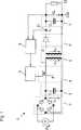
In
Die Eingangsspannung UE wird durch einen Gleichrichter
Mit der Gleichspannung U1 wird über eine Schaltstufe
Die Wechselspannung U3 wird mit dem Transformator
Die Ausgangsspannung der sekundärseitigen Glättungsbaugruppe
Damit die Ausgangsspannung UA auch bei sich ändernder Last
Neben dieser Spannungsregelung ist zusätzlich eine Stromregelung derart vorgesehen, dass ein am Ausgang des Schaltnetzteils
Ein solches Schaltnetzteil
Sekundärseitig kann der Transformator
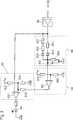
Die Regelschaltung
Das von dem Auswerteverstärker
Weiterhin ist der invertierende Eingang des Operationsverstärkers
Wenn am Ausgang des ersten Operationsverstärkers
Die zweite Vergleichsstufe
Die zweite Vergleichsstufe
Konkret wird bei einem Überschreiten des zweiten Vergleichswertes am Eingang der zweiten Vergleichsstufe
Die Umschaltung zwischen den beiden Maximalströmen I‘max, Imax wird über eine Integratorschaltung
Die Integratorschaltung
Der Ausgang der Integratorschaltung
Diese Spannung am Ausgang der Integratorschaltung
Wenn im Fehlerfall der Ausgangsstrom IA zwar auf einen Stromwert ansteigt, der über dem regulären Maximalstrom Imax liegt, nicht jedoch den erhöhten Maximalstrom I’max erreicht, wird es entsprechend länger dauern, bis die Spannung am Ausgang der Integratorschaltung
Die Zeitcharakteristik der Strombegrenzerschaltung ermöglicht auch das Treiben von Lasten mit hohem Anlaufstrom wie dies typischerweise bei Motorlasten oder kapazitiven Lasten gegeben ist. Ein Motoranlaufstrom im Bereich von beispielsweise dem 2,5-fachen des Nennstromes des Schaltnetzteils
Wenn, entweder durch Auslösen der nachgeschalteten Sicherung oder durch ein Beheben des Fehlerfalls, der Ausgangsstrom IA am Ausgang des Schaltnetzteils
Im Unterschied zum Ausführungsbeispiel der
BezugszeichenlisteLIST OF REFERENCE NUMBERS
- 11
- SchaltnetzteilSwitching Power Supply
- 22
- Gleichrichterrectifier
- 33
- Glättungsbaugruppesmoothing assembly
- 44
- Schaltstufeswitching stage
- 4141
- Schaltorganswitching element
- 55
- Transformatortransformer
- 66
- ausgangsseitiger Gleichrichteroutput rectifier
- 77
- ausgangsseitige Glättungsbaugruppeoutput-side smoothing module
- 88th
- Regelschaltungcontrol circuit
- 8181
- Stromsensorcurrent sensor
- 8282
- Auswerteverstärkeranalysis amplifier
- 8383
- erste Vergleichsstufefirst comparison stage
- 8484
- zweite Vergleichsstufesecond comparison stage
- 8585
- Integratorschaltungintegrator circuit
- 8686
- Optokoppleroptocoupler
- 831831
- Operationsverstärkeroperational amplifiers
- 832 bis 834832-834
- Widerstandresistance
- 841841
- Operationsverstärker /VergleicherOperational amplifier / comparator
- 842, 843842, 843
- Widerstandresistance
- 851851
- Ladewiderstandload resistance
- 852852
- Diodediode
- 853853
- Entladewiderstanddischarge
- 854854
- weitere Diodeanother diode
- 855855
- Kondensatorcapacitor
- 99
- PWM-SchaltungPWM circuit
- 1010
- Lastload
- C1, C2C1 , C2
- Glättungskondensatorsmoothing capacitor
- UEUE
- Eingangsspannunginput voltage
- UAUA
- Ausgangsspannungoutput voltage
- U1U1
- GleichspannungDC
- U2U2
- Primärspannungprimary voltage
- U3U3
- Sekundärspannungsecondary voltage
- UrefUref
- Referenzspannungreference voltage
- GNDGND
- Bezugspotentialreference potential
- II
- Primärseite des Transformators / des NetzteilsPrimary side of the transformer / power supply
- IIII
- Sekundärseite des Transformators / des NetzteilsSecondary side of the transformer / power supply
- InennIcall
- AusgangsnennstromNominal output current
- ImaxImax
- regulärer Maximalstromregular maximum current
- I'maxI 'max
- erhöhter Maximalstromincreased maximum current
ZITATE ENTHALTEN IN DER BESCHREIBUNG QUOTES INCLUDE IN THE DESCRIPTION
Diese Liste der vom Anmelder aufgeführten Dokumente wurde automatisiert erzeugt und ist ausschließlich zur besseren Information des Lesers aufgenommen. Die Liste ist nicht Bestandteil der deutschen Patent- bzw. Gebrauchsmusteranmeldung. Das DPMA übernimmt keinerlei Haftung für etwaige Fehler oder Auslassungen.This list of the documents listed by the applicant has been generated automatically and is included solely for the better information of the reader. The list is not part of the German patent or utility model application. The DPMA assumes no liability for any errors or omissions.
Zitierte PatentliteraturCited patent literature
- DE 102005031833 A1[0007]DE 102005031833 A1[0007]
Claims (14)
Translated fromGermanPriority Applications (7)
| Application Number | Priority Date | Filing Date | Title |
|---|---|---|---|
| DE102013113648.6ADE102013113648A1 (en) | 2013-12-06 | 2013-12-06 | Power supply device and method for limiting an output current of a power supply device |
| US15/033,041US9941782B2 (en) | 2013-12-06 | 2014-11-18 | Power supply device and method for limiting an output current of a power supply device |
| ES14800027TES2781108T3 (en) | 2013-12-06 | 2014-11-18 | Power supply device and procedure for limiting the output current of the power supply device |
| CN201480066151.5ACN105794095B (en) | 2013-12-06 | 2014-11-18 | Power supply device and method for limiting output current of the power supply device |
| PL14800027TPL3078105T3 (en) | 2013-12-06 | 2014-11-18 | Power supply device and method for limiting an output current of a power supply device |
| EP14800027.6AEP3078105B1 (en) | 2013-12-06 | 2014-11-18 | Power supply device and method for limiting an output current of a power supply device |
| PCT/EP2014/074839WO2015082207A1 (en) | 2013-12-06 | 2014-11-18 | Power supply device and method for limiting an output current of a power supply device |
Applications Claiming Priority (1)
| Application Number | Priority Date | Filing Date | Title |
|---|---|---|---|
| DE102013113648.6ADE102013113648A1 (en) | 2013-12-06 | 2013-12-06 | Power supply device and method for limiting an output current of a power supply device |
Publications (1)
| Publication Number | Publication Date |
|---|---|
| DE102013113648A1true DE102013113648A1 (en) | 2015-06-11 |
Family
ID=51932339
Family Applications (1)
| Application Number | Title | Priority Date | Filing Date |
|---|---|---|---|
| DE102013113648.6APendingDE102013113648A1 (en) | 2013-12-06 | 2013-12-06 | Power supply device and method for limiting an output current of a power supply device |
Country Status (7)
| Country | Link |
|---|---|
| US (1) | US9941782B2 (en) |
| EP (1) | EP3078105B1 (en) |
| CN (1) | CN105794095B (en) |
| DE (1) | DE102013113648A1 (en) |
| ES (1) | ES2781108T3 (en) |
| PL (1) | PL3078105T3 (en) |
| WO (1) | WO2015082207A1 (en) |
Cited By (4)
| Publication number | Priority date | Publication date | Assignee | Title |
|---|---|---|---|---|
| DE102018108678A1 (en) | 2018-04-12 | 2019-10-17 | Hubert Fetscher | Multi-channel switched-mode power supply with line protection |
| DE102018124191A1 (en)* | 2018-10-01 | 2020-04-02 | Wago Verwaltungsgesellschaft Mbh | power adapter |
| DE102020203469A1 (en) | 2020-03-18 | 2021-09-23 | Thyssenkrupp Ag | Method for operating a lithium accumulator on an on-board network designed for lead accumulators in a submarine |
| DE102021126399A1 (en) | 2021-10-12 | 2023-04-13 | WAGO Verwaltungsgesellschaft mit beschränkter Haftung | Process and circuit arrangement for controlling a switched-mode power supply |
Families Citing this family (13)
| Publication number | Priority date | Publication date | Assignee | Title |
|---|---|---|---|---|
| DE102015105476A1 (en)* | 2015-04-10 | 2016-10-13 | Abb Schweiz Ag | Method and device for supplying power to a low-voltage load |
| US10270241B2 (en)* | 2016-05-16 | 2019-04-23 | Varian Semiconductor Equipment Associates, Inc. | Fault current limiter having fault checking system for power electronics and bypass circuit |
| CN107069669B (en)* | 2016-12-22 | 2019-04-19 | 中国人民解放军海军工程大学 | DC converter overcurrent protection method |
| US10277111B2 (en)* | 2017-05-24 | 2019-04-30 | Infineon Technologies Ag | Output overvoltage protection for converters |
| CN109995225B (en)* | 2017-12-29 | 2021-06-01 | 技嘉科技股份有限公司 | Power supply with adjustable power consumption limit and method for adjusting power consumption limit |
| BE1026994B1 (en) | 2019-01-29 | 2020-08-24 | Phoenix Contact Gmbh & Co | Power supply device and method for the regulated energy supply of at least one electrical consumer |
| WO2020152340A1 (en) | 2019-01-25 | 2020-07-30 | Phoenix Contact Gmbh & Co.Kg | Power supply device and method for supplying power in a controlled fashion to at least one electric load |
| DE102019101939A1 (en) | 2019-01-25 | 2020-07-30 | Phoenix Contact Gmbh & Co. Kg | Power supply device and method for regulated energy supply of at least one electrical consumer |
| CA3185609A1 (en)* | 2020-05-29 | 2021-12-02 | Abl Ip Holding Llc | Flyback converter with indirect estimation of primary-side voltage at the secondary-side |
| CN113889991B (en)* | 2020-07-03 | 2024-07-12 | 圣邦微电子(北京)股份有限公司 | Short-circuit protection circuit and short-circuit protection method |
| US11322930B1 (en)* | 2020-10-20 | 2022-05-03 | Lear Corporation | Electrical system including a power distribution circuit |
| CN115347539B (en)* | 2021-05-13 | 2025-02-18 | 固纬电子实业股份有限公司 | Current limiting circuit for power supply device |
| TWI771002B (en)* | 2021-05-13 | 2022-07-11 | 固緯電子實業股份有限公司 | Current limiting circuits for power supply units |
Citations (4)
| Publication number | Priority date | Publication date | Assignee | Title |
|---|---|---|---|---|
| DE19740932A1 (en)* | 1997-09-17 | 1999-04-01 | Siemens Ag | Circuit arrangement for determining the output power of a switching power supply |
| DE19962615A1 (en)* | 1999-12-23 | 2001-07-05 | Daimler Chrysler Ag | Device and method for converter overload protection |
| DE60119474T2 (en)* | 2000-10-20 | 2006-12-14 | Smk Corp. | Intermittent switching power supply |
| DE102005031833A1 (en) | 2005-07-06 | 2007-01-18 | Phoenix Contact Gmbh & Co. Kg | Method and electronic power supply device for supplying power to a low-voltage load protected by a protective device |
Family Cites Families (13)
| Publication number | Priority date | Publication date | Assignee | Title |
|---|---|---|---|---|
| DE3150398C2 (en)* | 1981-12-16 | 1985-08-29 | Siemens AG, 1000 Berlin und 8000 München | Intrinsically safe power supply device with a controllable semiconductor arranged in the primary circuit of a transformer |
| WO1998013918A1 (en)* | 1996-09-24 | 1998-04-02 | Siemens Aktiengesellschaft | Circuit arrangement to provide electronic tripping devices with an electricity supply |
| DE10019329A1 (en)* | 2000-04-19 | 2001-10-25 | Abb Patent Gmbh | Switching power supply with regulated output voltage |
| DE10214190B4 (en)* | 2002-03-28 | 2011-06-30 | Minebea Co., Ltd. | Power supply with several parallel switching power supplies |
| US7106037B2 (en)* | 2003-07-02 | 2006-09-12 | Toko, Inc. | Switching-type constant current power supply device |
| JP2005086931A (en)* | 2003-09-10 | 2005-03-31 | Renesas Technology Corp | Switching power supply and semiconductor integrated circuit used for it |
| GB2430051B (en)* | 2004-06-23 | 2009-01-07 | Salcomp Oyj | Method and circuit for limiting output voltage in a switched-mode power supply and a switched-mode power supply |
| CN1734875A (en)* | 2004-08-02 | 2006-02-15 | 国际整流器公司 | Electronic circuit protection device with i2t or other function |
| US7619865B2 (en)* | 2004-08-02 | 2009-11-17 | International Rectifier Corporation | Electronic circuit protection device with I2t or other function |
| US7342762B2 (en)* | 2005-11-10 | 2008-03-11 | Littelfuse, Inc. | Resettable circuit protection apparatus |
| EP2093874A1 (en)* | 2008-02-21 | 2009-08-26 | Siemens Aktiengesellschaft | Power supply, particularly for redundant operation with several power supplies coupled in parallel at the output |
| JP5679828B2 (en)* | 2010-02-09 | 2015-03-04 | キヤノン株式会社 | Switching power supply and image forming apparatus |
| JP5904245B2 (en)* | 2014-08-28 | 2016-04-13 | Tdk株式会社 | Power supply control circuit and power supply device |
- 2013
- 2013-12-06DEDE102013113648.6Apatent/DE102013113648A1/enactivePending
- 2014
- 2014-11-18WOPCT/EP2014/074839patent/WO2015082207A1/enactiveApplication Filing
- 2014-11-18CNCN201480066151.5Apatent/CN105794095B/enactiveActive
- 2014-11-18ESES14800027Tpatent/ES2781108T3/enactiveActive
- 2014-11-18USUS15/033,041patent/US9941782B2/enactiveActive
- 2014-11-18EPEP14800027.6Apatent/EP3078105B1/enactiveActive
- 2014-11-18PLPL14800027Tpatent/PL3078105T3/enunknown
Patent Citations (4)
| Publication number | Priority date | Publication date | Assignee | Title |
|---|---|---|---|---|
| DE19740932A1 (en)* | 1997-09-17 | 1999-04-01 | Siemens Ag | Circuit arrangement for determining the output power of a switching power supply |
| DE19962615A1 (en)* | 1999-12-23 | 2001-07-05 | Daimler Chrysler Ag | Device and method for converter overload protection |
| DE60119474T2 (en)* | 2000-10-20 | 2006-12-14 | Smk Corp. | Intermittent switching power supply |
| DE102005031833A1 (en) | 2005-07-06 | 2007-01-18 | Phoenix Contact Gmbh & Co. Kg | Method and electronic power supply device for supplying power to a low-voltage load protected by a protective device |
Non-Patent Citations (1)
| Title |
|---|
| Infineon: TDA16846/7, Datenblatt. München, 2000. - Firmenschrift* |
Cited By (7)
| Publication number | Priority date | Publication date | Assignee | Title |
|---|---|---|---|---|
| DE102018108678A1 (en) | 2018-04-12 | 2019-10-17 | Hubert Fetscher | Multi-channel switched-mode power supply with line protection |
| DE102018124191A1 (en)* | 2018-10-01 | 2020-04-02 | Wago Verwaltungsgesellschaft Mbh | power adapter |
| DE102020203469A1 (en) | 2020-03-18 | 2021-09-23 | Thyssenkrupp Ag | Method for operating a lithium accumulator on an on-board network designed for lead accumulators in a submarine |
| WO2021185630A1 (en) | 2020-03-18 | 2021-09-23 | Thyssenkrupp Marine Systems Gmbh | Method for operating a lithium storage battery in an on-board electrical system designed for lead batteries in a submarine |
| DE102021126399A1 (en) | 2021-10-12 | 2023-04-13 | WAGO Verwaltungsgesellschaft mit beschränkter Haftung | Process and circuit arrangement for controlling a switched-mode power supply |
| EP4167457A1 (en) | 2021-10-12 | 2023-04-19 | WAGO Verwaltungsgesellschaft mbH | Method and circuit arrangement for controlling a switched mode power supply |
| US12244221B2 (en) | 2021-10-12 | 2025-03-04 | Wago Verwaltungsgesellschaft Mbh | Method and circuit arrangement for controlling a switched-mode power supply |
Also Published As
| Publication number | Publication date |
|---|---|
| CN105794095A (en) | 2016-07-20 |
| ES2781108T3 (en) | 2020-08-28 |
| US20160285356A1 (en) | 2016-09-29 |
| EP3078105A1 (en) | 2016-10-12 |
| PL3078105T3 (en) | 2020-06-29 |
| EP3078105B1 (en) | 2019-12-25 |
| US9941782B2 (en) | 2018-04-10 |
| WO2015082207A1 (en) | 2015-06-11 |
| CN105794095B (en) | 2018-09-25 |
Similar Documents
| Publication | Publication Date | Title |
|---|---|---|
| DE102013113648A1 (en) | Power supply device and method for limiting an output current of a power supply device | |
| DE102009036861B4 (en) | Method for controlling a voltage converter, voltage converter and operating device with a voltage converter | |
| DE102013105485A1 (en) | Control for a power converter and method of operation thereof | |
| DE102016102417B4 (en) | Protection circuit for a photovoltaic (PV) module, method for operating the protection circuit and photovoltaic (PV) system with such a protection circuit | |
| DE112007000411T5 (en) | Power supply controller | |
| DE102015105488A1 (en) | SYSTEM AND METHOD FOR A CONTACTED POWER SUPPLY | |
| DE102013105475A1 (en) | Control for a power converter and method of operation thereof | |
| DE19916915B4 (en) | Switching power supply and method for determining the supply voltage in a switched-mode power supply | |
| EP1081839A2 (en) | Series resonant converter with a regulation circuit | |
| EP0134505B1 (en) | High voltage direct current supply with overcurrent protection | |
| DE2513005A1 (en) | STABILIZED POWER SUPPLY | |
| DE3713540A1 (en) | COMBINED SECONDARY SWITCH | |
| DE69733679T2 (en) | Switching Power Supply | |
| DE102014214984A1 (en) | Short-circuit protection device | |
| DE102011053013A1 (en) | Symmetrical device for balancing voltage division of serially-connected energy storage devices e.g. capacitors, has control unit that drives switch element of bypass circuit according to voltage requirement of energy storage device | |
| DE3123804A1 (en) | OVERLOAD PROTECTION CIRCUIT FOR POWER SUPPLIES | |
| EP0193723A1 (en) | Current supervision for a switching regulator | |
| DE102010036421B4 (en) | Overcurrent protection for DC converters | |
| DE60318889T2 (en) | POWER SUPPLY | |
| DE102014202617B4 (en) | Method and device for measuring a battery cell current | |
| DE2838009B1 (en) | Current limiting circuit for a DC converter | |
| DE60014357T2 (en) | Start-up circuit for switching power supplies | |
| DE102016220199A1 (en) | DC-DC converter and method for operating a DC-DC converter | |
| DE102017205127B4 (en) | PWM-controlled loop with anti-accumulation protection | |
| EP0402367B1 (en) | Active filter |
Legal Events
| Date | Code | Title | Description |
|---|---|---|---|
| R163 | Identified publications notified | ||
| R012 | Request for examination validly filed | ||
| R016 | Response to examination communication |