DE102013111433A1 - Planar balanced coil for integrated RF circuits - Google Patents
Planar balanced coil for integrated RF circuitsDownload PDFInfo
- Publication number
- DE102013111433A1 DE102013111433A1DE102013111433.4ADE102013111433ADE102013111433A1DE 102013111433 A1DE102013111433 A1DE 102013111433A1DE 102013111433 ADE102013111433 ADE 102013111433ADE 102013111433 A1DE102013111433 A1DE 102013111433A1
- Authority
- DE
- Germany
- Prior art keywords
- coil
- planar
- integrated
- parts
- circuits
- Prior art date
- Legal status (The legal status is an assumption and is not a legal conclusion. Google has not performed a legal analysis and makes no representation as to the accuracy of the status listed.)
- Withdrawn
Links
- 238000004804windingMethods0.000claimsabstractdescription8
- 238000001465metallisationMethods0.000claimsdescription13
- 239000004020conductorSubstances0.000claimsdescription12
- 230000008878couplingEffects0.000description3
- 238000010168coupling processMethods0.000description3
- 238000005859coupling reactionMethods0.000description3
- 230000003071parasitic effectEffects0.000description3
- 230000000694effectsEffects0.000description2
- 230000005684electric fieldEffects0.000description2
- 239000000463materialSubstances0.000description2
- BUHVIAUBTBOHAG-FOYDDCNASA-N(2r,3r,4s,5r)-2-[6-[[2-(3,5-dimethoxyphenyl)-2-(2-methylphenyl)ethyl]amino]purin-9-yl]-5-(hydroxymethyl)oxolane-3,4-diolChemical compoundCOC1=CC(OC)=CC(C(CNC=2C=3N=CN(C=3N=CN=2)[C@H]2[C@@H]([C@H](O)[C@@H](CO)O2)O)C=2C(=CC=CC=2)C)=C1BUHVIAUBTBOHAG-FOYDDCNASA-N0.000description1
- 238000013459approachMethods0.000description1
- 230000002500effect on skinEffects0.000description1
- 239000002184metalSubstances0.000description1
- 238000000034methodMethods0.000description1
- 238000004377microelectronicMethods0.000description1
Images

Classifications
- H—ELECTRICITY
- H01—ELECTRIC ELEMENTS
- H01F—MAGNETS; INDUCTANCES; TRANSFORMERS; SELECTION OF MATERIALS FOR THEIR MAGNETIC PROPERTIES
- H01F17/00—Fixed inductances of the signal type
- H01F17/0006—Printed inductances
- H—ELECTRICITY
- H01—ELECTRIC ELEMENTS
- H01F—MAGNETS; INDUCTANCES; TRANSFORMERS; SELECTION OF MATERIALS FOR THEIR MAGNETIC PROPERTIES
- H01F17/00—Fixed inductances of the signal type
- H01F17/0006—Printed inductances
- H01F2017/0053—Printed inductances with means to reduce eddy currents
- H—ELECTRICITY
- H01—ELECTRIC ELEMENTS
- H01F—MAGNETS; INDUCTANCES; TRANSFORMERS; SELECTION OF MATERIALS FOR THEIR MAGNETIC PROPERTIES
- H01F17/00—Fixed inductances of the signal type
- H01F17/0006—Printed inductances
- H01F2017/0073—Printed inductances with a special conductive pattern, e.g. flat spiral
Landscapes
- Engineering & Computer Science (AREA)
- Power Engineering (AREA)
- Microelectronics & Electronic Packaging (AREA)
- Coils Or Transformers For Communication (AREA)
Abstract
Translated fromGermanDescription
Translated fromGermanDie Erfindung betrifft eine planare symmetrische Spule für integrierte HF-Schaltungen, die zwei Spulenteile mit je einem Anfang und einem Ende umfasst, wobei mit den beiden Spulenteilen eine ungerade Anzahl von Spulenwindungen ausbildbar ist.The invention relates to a planar symmetrical coil for integrated RF circuits, comprising two coil parts each having a start and an end, wherein an odd number of coil turns can be formed with the two coil parts.
In der Mikroelektronik können Induktivitäten als planare Spulen realisiert werden. Aufgrund ihrer kleinen Induktivitäten und der geringen Güte kommen sie erst im HF-Bereich als zusätzliches Bauelement in Betracht. Dabei können integrierte Spulen zur Kompensation von parasitären Kapazitäten oder in einem Schwingkreis eingesetzt werden.Inductors can be realized as planar coils in microelectronics. Due to their small inductances and the low quality they are only in the RF range as an additional component into consideration. In this case, integrated coils can be used to compensate for parasitic capacitances or in a resonant circuit.
Die Spulen stellen dabei die Schlüsselkomponenten für energieeffiziente HF-Schaltung dar. Nur so sind energieeffiziente und leitungsfähige Transmitter und Receiver möglich. Jedoch wird das Verhalten der Spule durch viele parasitäre Effekte beeinflusst.The coils represent the key components for energy-efficient RF switching. Only then are energy-efficient and conductive transmitters and receivers possible. However, the behavior of the coil is influenced by many parasitic effects.
Bei niedrigen Frequenzen ist dies vor allem die begrenzte Leitfähigkeit des Leitermaterials, welche in Kombination mit sehr dünnen Schichtdicken der Metallisierungsebenen relativ große Widerstände der Leiterbahnen ergeben. Mit zunehmender Frequenz steigt nicht nur der Einfluss des Skineffektes, sondern die Stromverteilung wird auch durch das zwischen benachbarten Wicklungen entstehende Magnetfeld weiter beeinflusst, wodurch der effektive Leiterquerschnitt verringert und dadurch der Widerstand der Leiterbahn vergrößert wird und damit die elektrischen Verluste steigen.At low frequencies, this is above all the limited conductivity of the conductor material, which, in combination with very thin layer thicknesses of the metallization levels, results in relatively large resistances of the conductor tracks. As the frequency increases, not only does the effect of the skin effect increase, but the current distribution is further affected by the magnetic field generated between adjacent windings, thereby reducing the effective conductor cross-section and thereby increasing the resistance of the trace and thus increasing electrical losses.
Das Verhalten der Spule wird auch durch kapazitive Kopplungen zwischen den Leitern beeinflusst. So wirkt sich bei einer planaren, spiralförmigen Spule die Überlappung zwischen den Leiterbahnen der Spule mit derjenigen die vom inneren Anschluss nach außen geführt wird, kapazitiv aus, wohingegen der windungsbedingte kapazitive Anteil zwischen den benachbarten Windungen vernachlässigt werden kann.The behavior of the coil is also affected by capacitive couplings between the conductors. Thus, in a planar helical coil, the overlap between the conductor tracks of the coil and that which leads outwardly from the inner terminal will have a capacitive effect, whereas the winding-related capacitive component between the adjacent turns may be neglected.
Im bisherigen Stand der Technik wurden verschiedene Ansätze verfolgt, die parasitären Effekte zu reduzieren, um die Spulengüte zu verbessern. Beispielsweise wurden, um den Serienwiderstand zu senken, mehrere Metallisierungsebenen parallelgeschaltet oder abweichend vom CMOS-Prozess andere Leitermaterialien eingesetzt, die einen geringeren spezifischen Widerstand aufweisen, wodurch die Verlustleistung verringert und damit eine höhere Güte erreicht wurde.In the prior art, various approaches have been taken to reduce the parasitic effects in order to improve the coil quality. For example, in order to reduce the series resistance, several metallization levels have been connected in parallel or, unlike the CMOS process, other conductor materials have been used which have a lower resistivity, thereby reducing the power loss and thus achieving a higher quality.
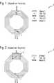
Ein weiterer Nachteil der bisher beschriebenen planaren, spiralförmigen Spulen ist auch das asymmetrische Verhalten bezüglich der Spulenanschlüsse aufgrund des asymmetrischen Aufbaus. Um identische Spulen-Charakteristika von beiden Spulenanschlüssen aus gesehen, zu realisieren, kann beispielsweise eine symmetrische Spule durch das Zusammenschalten von zwei asymmetrischen Spulen realisiert oder ein konventionelles Spulenlayout gemäß
Die Verwendung von zwei asymmetrischen Spulen hat aber den Nachteil, dass keine Kopplung zwischen den Spulen besteht, wodurch der Platzbedarf größer wird. Des Weiteren ist die Kopplung der Spulen für einige Schaltungen sehr hilfreich, da dadurch eine gezielte Fehlanpassung für unerwünschte Frequenzen oder Signalkomponenten erreicht werden kann.However, the use of two asymmetric coils has the disadvantage that there is no coupling between the coils, which increases the space required. Furthermore, the coupling of the coils is very helpful for some circuits, as this can be a targeted mismatch for unwanted frequencies or signal components can be achieved.
Die in
Des Weiteren benötigt das konventionelle Spulenlayout einer symmetrischen Spule entweder drei Metallisierungsebenen oder es bildet sich ein Kurzschlussring aus (
In der
In der
Es ist daher Aufgabe der Erfindung, ein Spulenlayout bzw. ein Wickelschema für eine planare symmetrische Spule anzugeben, das die oben genannten Nachteile umgeht und mit welchem Spulen mit einer höheren Graduierung der einzustellenden Induktivität realisiert werden können.It is therefore an object of the invention to provide a coil layout or a winding scheme for a planar symmetrical coil, which circumvents the above-mentioned disadvantages and with which coils can be realized with a higher graduation of the inductor to be set.
Die Aufgabe der Erfindung wird dadurch gelöst, dass die Enden der zwei Spulenteile nichtleitend gekreuzt werden und in zwei weiteren Spulenteilen neben die Anfangsanschlüsse der ersten zwei Spulenteile geführt werden und eine gerade Anzahl von Spulenwindungen ausbilden. The object of the invention is achieved in that the ends of the two coil parts are non-conducting crossed and are performed in two other coil parts in addition to the initial connections of the first two coil parts and form an even number of coil turns.
Vor allem in integrierten HF-Schaltungen ist oft eine feine Graduierung der einzusetzenden Induktivitäten notwendig, was durch die vorliegende Erfindung möglich wird, da im bisherigen Stand der Technik die Anzahl der Spulenwindungen auf eine ungerade Anzahl, d.h. drei, fünf usw. Windungen beschränkt war und nun mit der Abstufung von zwei-drei-vier-fünf-sechs usw. Spulenwindungen eine wesentlich feinere Abstufung realisierbar wird.Especially in integrated RF circuits, a fine graduation of the inductors to be used is often necessary, which is made possible by the present invention, since in the prior art, the number of turns of coils to an odd number, i.e.. three, five, etc. turns, and now with the grading of two-three-four-five-six, etc. coil turns, a much finer gradation becomes feasible.
Der Vorteil dieser Spulenausbildung ist, dass die planare symmetrische Spule nur maximal zwei Metallisierungsebenen benötigt und alle Anschlüsse der Spule nebeneinander auf einer Seite und außerhalb des Spulenkörpers angeordnet werden können. Damit können die Gleichstromverluste gegenüber einer konventionellen Umsetzung verringert werden.The advantage of this coil design is that the planar symmetrical coil requires only a maximum of two metallization levels and all connections of the coil can be arranged side by side on one side and outside of the coil former. Thus, the DC losses can be reduced compared to a conventional implementation.
In der vorliegenden Erfindung sind die Kreuzungen der Spulenwindungen nur zwischen benachbarten Leitern ausgebildet, wobei an den Kreuzungen ein Wechsel zwischen den Metallisierungsebenen erfolgt. Damit lässt sich das Wickelschema sehr leicht und einfach umsetzen und die Spannungsamplitude zwischen benachbarten Leitern kann reduziert werden, so dass die elektrische Energie verringert und die Selbstresonanzfrequenz der Spule erhöht wird. Diese ist typischerweise mehr als 30% größer als im Vergleich zu der konventionellen Umsetzung. Durch die Erhöhung der Selbstresonanzfrequenz steigt auch die Spulengüte.In the present invention, the intersections of the coil turns are formed only between adjacent conductors, wherein at the intersections a change takes place between the metallization levels. Thus, the winding scheme can be very easily and simply implemented and the voltage amplitude between adjacent conductors can be reduced, so that the electrical energy is reduced and the self-resonant frequency of the coil is increased. This is typically more than 30% larger than compared to the conventional implementation. Increasing the self-resonant frequency also increases the coil quality.
Die Spulenteile der planaren Spule sind symmetrisch entlang einer in einer parallel zu den Metallisierungsebenen gedachten Spulenebene liegenden Achse angeordnet. Damit liegen identische Spulen-Charakteristika von beiden Spulenanschlüssen aus gesehen vor.The coil parts of the planar coil are arranged symmetrically along an axis lying in a plane parallel to the metallization planes imaginary axis. Thus, identical coil characteristics are seen from both coil terminals.
Die Spulenwindungen in der Spulenebene können eine quadratische oder eine oktogonale oder eine andere symmetrisch zur Symmetrieachse der Spule ausgebildete Form aufweisen.The coil windings in the coil plane may have a square or an octagonal or another symmetrical shape to the symmetry axis of the coil formed shape.
Die Erfindung soll nachfolgend anhand eines Ausführungsbeispiels näher erläutert werden.The invention will be explained in more detail with reference to an embodiment.
Die zugehörigen Zeichnungen zeigenThe accompanying drawings show
a) in Parallelschaltung
b) in Serienschaltung.
a) in parallel
b) connected in series.
Die erfindungsgemäße planare symmetrische Spule kann z.B. in Verstärkerschaltungen eingesetzt werden, wobei mit der größeren Spulengüte eine große Verstärkung und höhere Wirkungsgrade erzielt werden können.The planar symmetrical coil according to the invention may e.g. be used in amplifier circuits, with the larger package quality a large gain and higher efficiencies can be achieved.
Das erfindungsgemäße Spulenlayout ist überall dort einsetzbar, wo bisher Spulen mit konventionellem Layout eingesetzt werden. Sie sind aber nicht darauf beschränkt.The coil layout according to the invention can be used everywhere, where previously coils are used with conventional layout. But you are not limited to that.
Bezugszeichenliste LIST OF REFERENCE NUMBERS
- MM
- Mittenanschlusscenter connection
- P, NP, N
- Anfangsanschlussinitial lead
- P2, N2P2, N2
- EndanschlüsseEnd Connections
- 11
- Kreuzung der SpulenleiterCrossing of the coil conductors
- 22
- KurzschlussringShorting ring
- 33
- planare symmetrische Spulenplanar symmetrical coils
ZITATE ENTHALTEN IN DER BESCHREIBUNG QUOTES INCLUDE IN THE DESCRIPTION
Diese Liste der vom Anmelder aufgeführten Dokumente wurde automatisiert erzeugt und ist ausschließlich zur besseren Information des Lesers aufgenommen. Die Liste ist nicht Bestandteil der deutschen Patent- bzw. Gebrauchsmusteranmeldung. Das DPMA übernimmt keinerlei Haftung für etwaige Fehler oder Auslassungen.This list of the documents listed by the applicant has been generated automatically and is included solely for the better information of the reader. The list is not part of the German patent or utility model application. The DPMA assumes no liability for any errors or omissions.
Zitierte PatentliteraturCited patent literature
- JP 2005191217 A[0011]JP 2005191217A[0011]
- WO 2011004803 A1[0012]WO 2011004803 A1[0012]
- US 2010164667 A1[0012]US 2010164667 A1[0012]
Claims (5)
Translated fromGermanPriority Applications (1)
| Application Number | Priority Date | Filing Date | Title |
|---|---|---|---|
| DE102013111433.4ADE102013111433A1 (en) | 2013-08-30 | 2013-10-17 | Planar balanced coil for integrated RF circuits |
Applications Claiming Priority (3)
| Application Number | Priority Date | Filing Date | Title |
|---|---|---|---|
| DE102013109485 | 2013-08-30 | ||
| DE102013109485.6 | 2013-08-30 | ||
| DE102013111433.4ADE102013111433A1 (en) | 2013-08-30 | 2013-10-17 | Planar balanced coil for integrated RF circuits |
Publications (1)
| Publication Number | Publication Date |
|---|---|
| DE102013111433A1true DE102013111433A1 (en) | 2015-03-05 |
Family
ID=52470236
Family Applications (1)
| Application Number | Title | Priority Date | Filing Date |
|---|---|---|---|
| DE102013111433.4AWithdrawnDE102013111433A1 (en) | 2013-08-30 | 2013-10-17 | Planar balanced coil for integrated RF circuits |
Country Status (1)
| Country | Link |
|---|---|
| DE (1) | DE102013111433A1 (en) |
Cited By (3)
| Publication number | Priority date | Publication date | Assignee | Title |
|---|---|---|---|---|
| CN106571211A (en)* | 2015-10-13 | 2017-04-19 | 瑞昱半导体股份有限公司 | Integrated inductance structure and integrated transformer structure |
| CN106710847A (en)* | 2015-07-15 | 2017-05-24 | 瑞昱半导体股份有限公司 | Planar transformer and balance-unbalance converter structure |
| CN108226830A (en)* | 2018-01-05 | 2018-06-29 | 重庆大学 | A kind of resonant element and its array structure for being used to strengthen RF energy |
Citations (6)
| Publication number | Priority date | Publication date | Assignee | Title |
|---|---|---|---|---|
| WO2003052780A1 (en)* | 2001-12-18 | 2003-06-26 | Infineon Technologies Ag | Inductive component |
| JP2005191217A (en) | 2003-12-25 | 2005-07-14 | Sharp Corp | Spiral inductor and circuit device or differential circuit including the same |
| WO2008014506A2 (en)* | 2006-07-28 | 2008-01-31 | Qualcomm Incorporated | Dual inductor circuit for multi-band wireless communication device |
| US20100164667A1 (en) | 2008-12-31 | 2010-07-01 | Taiwan Semiconductor Manufacturing Co., Ltd. | On-chip transformer balun structures |
| JP2010205939A (en)* | 2009-03-03 | 2010-09-16 | Asahi Kasei Electronics Co Ltd | Variable inductor, and voltage-controlled oscillator |
| WO2011004803A1 (en) | 2009-07-08 | 2011-01-13 | 株式会社村田製作所 | Coil component |
- 2013
- 2013-10-17DEDE102013111433.4Apatent/DE102013111433A1/ennot_activeWithdrawn
Patent Citations (6)
| Publication number | Priority date | Publication date | Assignee | Title |
|---|---|---|---|---|
| WO2003052780A1 (en)* | 2001-12-18 | 2003-06-26 | Infineon Technologies Ag | Inductive component |
| JP2005191217A (en) | 2003-12-25 | 2005-07-14 | Sharp Corp | Spiral inductor and circuit device or differential circuit including the same |
| WO2008014506A2 (en)* | 2006-07-28 | 2008-01-31 | Qualcomm Incorporated | Dual inductor circuit for multi-band wireless communication device |
| US20100164667A1 (en) | 2008-12-31 | 2010-07-01 | Taiwan Semiconductor Manufacturing Co., Ltd. | On-chip transformer balun structures |
| JP2010205939A (en)* | 2009-03-03 | 2010-09-16 | Asahi Kasei Electronics Co Ltd | Variable inductor, and voltage-controlled oscillator |
| WO2011004803A1 (en) | 2009-07-08 | 2011-01-13 | 株式会社村田製作所 | Coil component |
Cited By (4)
| Publication number | Priority date | Publication date | Assignee | Title |
|---|---|---|---|---|
| CN106710847A (en)* | 2015-07-15 | 2017-05-24 | 瑞昱半导体股份有限公司 | Planar transformer and balance-unbalance converter structure |
| CN106710847B (en)* | 2015-07-15 | 2019-04-26 | 瑞昱半导体股份有限公司 | Plane type transformer and balun structure |
| CN106571211A (en)* | 2015-10-13 | 2017-04-19 | 瑞昱半导体股份有限公司 | Integrated inductance structure and integrated transformer structure |
| CN108226830A (en)* | 2018-01-05 | 2018-06-29 | 重庆大学 | A kind of resonant element and its array structure for being used to strengthen RF energy |
Similar Documents
| Publication | Publication Date | Title |
|---|---|---|
| EP2462596B1 (en) | Current compensated inductor and method for producing a current compensated inductor | |
| WO2009012868A1 (en) | Plasma supply system | |
| EP0293617B1 (en) | High-frequency power transmitter | |
| DE3638748A1 (en) | CAPACITIVE DISCONNECT | |
| DE1292744B (en) | High voltage winding for transformers and reactors | |
| DE102013111433A1 (en) | Planar balanced coil for integrated RF circuits | |
| DE19927355A1 (en) | Transformer with capacitive resistor for operating with high inductivity consists of a low-retentivity magnet core with primary and secondary windings fitted around it. | |
| EP3207613A1 (en) | Coil assembly for inductive energy transmission, inductive energy-transmission device, and method for producing a coil assembly for inductive energy transmission | |
| DE1297217B (en) | Tube winding for transformers | |
| EP2863403B1 (en) | Transformer | |
| EP2495742B1 (en) | High-voltage resistant electricity-compensated interference suppression choke | |
| WO2015024901A1 (en) | Electrical resonance element for contactless inductive energy transmission | |
| DE102013204638A1 (en) | Device for detecting fault currents | |
| DE102011085085A1 (en) | Circuit arrangement for supplying energy for inductive heating to a fuel injection valve | |
| WO2020015962A1 (en) | Core assembly having magnetic properties for an electrical device, and throttle comprising such a core assembly | |
| CH639225A5 (en) | SEMICONDUCTOR CIRCUIT WITH AT LEAST ONE SERIES THROTTLE COIL, ESPECIALLY FOR ELECTRIC CONVERTERS. | |
| DE202013000831U1 (en) | transformer | |
| DE1282754B (en) | Circulator with concentrated switching elements for short electromagnetic waves | |
| DE19858506C2 (en) | Remote feed choke | |
| EP3729645B1 (en) | Lc-filter arrangement and electrical or electronical device comprising such an lc-filter arrangement | |
| EP3402062B1 (en) | Connection of at least two modular multilevel converters | |
| DE10238690B4 (en) | Arrangement for implementing a blocking impedance | |
| DE102007041592A1 (en) | Band capacitor coil for use in electric motor i.e. linear drive, has outer capacitor coil and inner capacitor coil wound with each other, where band capacitor coil is formed as compact air-core coil without coil core | |
| DE102012215862B4 (en) | Surface mount choke | |
| WO2024068181A1 (en) | Inductor, method for simulation, computer system, computer program product |
Legal Events
| Date | Code | Title | Description |
|---|---|---|---|
| R012 | Request for examination validly filed | ||
| R016 | Response to examination communication | ||
| R119 | Application deemed withdrawn, or ip right lapsed, due to non-payment of renewal fee |