DE102012210049A1 - Hybrid integrated component and method for its production - Google Patents
Hybrid integrated component and method for its productionDownload PDFInfo
- Publication number
- DE102012210049A1 DE102012210049A1DE102012210049ADE102012210049ADE102012210049A1DE 102012210049 A1DE102012210049 A1DE 102012210049A1DE 102012210049 ADE102012210049 ADE 102012210049ADE 102012210049 ADE102012210049 ADE 102012210049ADE 102012210049 A1DE102012210049 A1DE 102012210049A1
- Authority
- DE
- Germany
- Prior art keywords
- asic
- component
- mems
- substrate
- mems device
- Prior art date
- Legal status (The legal status is an assumption and is not a legal conclusion. Google has not performed a legal analysis and makes no representation as to the accuracy of the status listed.)
- Pending
Links
- 238000000034methodMethods0.000titleclaimsdescription26
- 238000004519manufacturing processMethods0.000titleclaimsdescription13
- 230000005291magnetic effectEffects0.000claimsabstractdescription34
- 239000000758substrateSubstances0.000claimsdescription91
- 235000012431wafersNutrition0.000claimsdescription22
- 229910052751metalInorganic materials0.000claimsdescription13
- 239000002184metalSubstances0.000claimsdescription13
- 230000008859changeEffects0.000claimsdescription6
- 238000009413insulationMethods0.000claimsdescription6
- 230000004907fluxEffects0.000claimsdescription5
- 230000001133accelerationEffects0.000claimsdescription4
- 238000011156evaluationMethods0.000claimsdescription4
- 239000004065semiconductorSubstances0.000claimsdescription4
- 238000001514detection methodMethods0.000claims1
- 239000010410layerSubstances0.000description50
- 230000008569processEffects0.000description14
- 238000012545processingMethods0.000description11
- 238000002161passivationMethods0.000description6
- 239000002346layers by functionSubstances0.000description5
- 229910001030Iron–nickel alloyInorganic materials0.000description4
- 238000010276constructionMethods0.000description4
- 238000005259measurementMethods0.000description4
- 230000010354integrationEffects0.000description3
- 239000000463materialSubstances0.000description3
- 238000007781pre-processingMethods0.000description3
- 239000003990capacitorSubstances0.000description2
- 239000004020conductorSubstances0.000description2
- 229910052802copperInorganic materials0.000description2
- 239000010949copperSubstances0.000description2
- 230000008021depositionEffects0.000description2
- 238000009429electrical wiringMethods0.000description2
- 238000005516engineering processMethods0.000description2
- 230000002349favourable effectEffects0.000description2
- 229910021420polycrystalline siliconInorganic materials0.000description2
- 125000006850spacer groupChemical group0.000description2
- BUHVIAUBTBOHAG-FOYDDCNASA-N(2r,3r,4s,5r)-2-[6-[[2-(3,5-dimethoxyphenyl)-2-(2-methylphenyl)ethyl]amino]purin-9-yl]-5-(hydroxymethyl)oxolane-3,4-diolChemical compoundCOC1=CC(OC)=CC(C(CNC=2C=3N=CN(C=3N=CN=2)[C@H]2[C@@H]([C@H](O)[C@@H](CO)O2)O)C=2C(=CC=CC=2)C)=C1BUHVIAUBTBOHAG-FOYDDCNASA-N0.000description1
- 229910003321CoFeInorganic materials0.000description1
- RYGMFSIKBFXOCR-UHFFFAOYSA-NCopperChemical compound[Cu]RYGMFSIKBFXOCR-UHFFFAOYSA-N0.000description1
- 229910019041PtMnInorganic materials0.000description1
- XUIMIQQOPSSXEZ-UHFFFAOYSA-NSiliconChemical compound[Si]XUIMIQQOPSSXEZ-UHFFFAOYSA-N0.000description1
- NRTOMJZYCJJWKI-UHFFFAOYSA-NTitanium nitrideChemical compound[Ti]#NNRTOMJZYCJJWKI-UHFFFAOYSA-N0.000description1
- 230000005290antiferromagnetic effectEffects0.000description1
- 230000004888barrier functionEffects0.000description1
- 239000002131composite materialSubstances0.000description1
- 238000013016dampingMethods0.000description1
- 230000001419dependent effectEffects0.000description1
- 238000005137deposition processMethods0.000description1
- 238000009792diffusion processMethods0.000description1
- 238000010292electrical insulationMethods0.000description1
- 230000007613environmental effectEffects0.000description1
- 238000005530etchingMethods0.000description1
- 230000005496eutecticsEffects0.000description1
- 230000005284excitationEffects0.000description1
- 239000012535impuritySubstances0.000description1
- 238000002955isolationMethods0.000description1
- 230000005415magnetizationEffects0.000description1
- 230000004048modificationEffects0.000description1
- 238000012986modificationMethods0.000description1
- 229910021421monocrystalline siliconInorganic materials0.000description1
- 239000002245particleSubstances0.000description1
- 238000000059patterningMethods0.000description1
- 229920005591polysiliconPolymers0.000description1
- 229910052707rutheniumInorganic materials0.000description1
- 230000035945sensitivityEffects0.000description1
- 238000000926separation methodMethods0.000description1
- 229910052710siliconInorganic materials0.000description1
- 239000010703siliconSubstances0.000description1
- 239000013589supplementSubstances0.000description1
- 239000010409thin filmSubstances0.000description1
- MAKDTFFYCIMFQP-UHFFFAOYSA-Ntitanium tungstenChemical compound[Ti].[W]MAKDTFFYCIMFQP-UHFFFAOYSA-N0.000description1
- WFKWXMTUELFFGS-UHFFFAOYSA-NtungstenChemical compound[W]WFKWXMTUELFFGS-UHFFFAOYSA-N0.000description1
- 229910052721tungstenInorganic materials0.000description1
- 239000010937tungstenSubstances0.000description1
Images


Classifications
- B—PERFORMING OPERATIONS; TRANSPORTING
- B81—MICROSTRUCTURAL TECHNOLOGY
- B81B—MICROSTRUCTURAL DEVICES OR SYSTEMS, e.g. MICROMECHANICAL DEVICES
- B81B3/00—Devices comprising flexible or deformable elements, e.g. comprising elastic tongues or membranes
- B81B3/0018—Structures acting upon the moving or flexible element for transforming energy into mechanical movement or vice versa, i.e. actuators, sensors, generators
- B—PERFORMING OPERATIONS; TRANSPORTING
- B81—MICROSTRUCTURAL TECHNOLOGY
- B81C—PROCESSES OR APPARATUS SPECIALLY ADAPTED FOR THE MANUFACTURE OR TREATMENT OF MICROSTRUCTURAL DEVICES OR SYSTEMS
- B81C1/00—Manufacture or treatment of devices or systems in or on a substrate
- B81C1/00015—Manufacture or treatment of devices or systems in or on a substrate for manufacturing microsystems
- B81C1/00222—Integrating an electronic processing unit with a micromechanical structure
- B81C1/00238—Joining a substrate with an electronic processing unit and a substrate with a micromechanical structure
- B—PERFORMING OPERATIONS; TRANSPORTING
- B81—MICROSTRUCTURAL TECHNOLOGY
- B81C—PROCESSES OR APPARATUS SPECIALLY ADAPTED FOR THE MANUFACTURE OR TREATMENT OF MICROSTRUCTURAL DEVICES OR SYSTEMS
- B81C1/00—Manufacture or treatment of devices or systems in or on a substrate
- B81C1/00015—Manufacture or treatment of devices or systems in or on a substrate for manufacturing microsystems
- B81C1/00222—Integrating an electronic processing unit with a micromechanical structure
- B81C1/00246—Monolithic integration, i.e. micromechanical structure and electronic processing unit are integrated on the same substrate
- B—PERFORMING OPERATIONS; TRANSPORTING
- B81—MICROSTRUCTURAL TECHNOLOGY
- B81C—PROCESSES OR APPARATUS SPECIALLY ADAPTED FOR THE MANUFACTURE OR TREATMENT OF MICROSTRUCTURAL DEVICES OR SYSTEMS
- B81C1/00—Manufacture or treatment of devices or systems in or on a substrate
- B81C1/00015—Manufacture or treatment of devices or systems in or on a substrate for manufacturing microsystems
- B81C1/00261—Processes for packaging MEMS devices
- B—PERFORMING OPERATIONS; TRANSPORTING
- B81—MICROSTRUCTURAL TECHNOLOGY
- B81C—PROCESSES OR APPARATUS SPECIALLY ADAPTED FOR THE MANUFACTURE OR TREATMENT OF MICROSTRUCTURAL DEVICES OR SYSTEMS
- B81C2203/00—Forming microstructural systems
- B81C2203/07—Integrating an electronic processing unit with a micromechanical structure
- B81C2203/0707—Monolithic integration, i.e. the electronic processing unit is formed on or in the same substrate as the micromechanical structure
- B81C2203/0735—Post-CMOS, i.e. forming the micromechanical structure after the CMOS circuit
- B—PERFORMING OPERATIONS; TRANSPORTING
- B81—MICROSTRUCTURAL TECHNOLOGY
- B81C—PROCESSES OR APPARATUS SPECIALLY ADAPTED FOR THE MANUFACTURE OR TREATMENT OF MICROSTRUCTURAL DEVICES OR SYSTEMS
- B81C2203/00—Forming microstructural systems
- B81C2203/07—Integrating an electronic processing unit with a micromechanical structure
- B81C2203/0707—Monolithic integration, i.e. the electronic processing unit is formed on or in the same substrate as the micromechanical structure
- B81C2203/0757—Topology for facilitating the monolithic integration
- B81C2203/0771—Stacking the electronic processing unit and the micromechanical structure
- B—PERFORMING OPERATIONS; TRANSPORTING
- B81—MICROSTRUCTURAL TECHNOLOGY
- B81C—PROCESSES OR APPARATUS SPECIALLY ADAPTED FOR THE MANUFACTURE OR TREATMENT OF MICROSTRUCTURAL DEVICES OR SYSTEMS
- B81C2203/00—Forming microstructural systems
- B81C2203/07—Integrating an electronic processing unit with a micromechanical structure
- B81C2203/0785—Transfer and j oin technology, i.e. forming the electronic processing unit and the micromechanical structure on separate substrates and joining the substrates
Landscapes
- Engineering & Computer Science (AREA)
- Manufacturing & Machinery (AREA)
- Microelectronics & Electronic Packaging (AREA)
- Chemical & Material Sciences (AREA)
- Analytical Chemistry (AREA)
- Computer Hardware Design (AREA)
- Micromachines (AREA)
- Pressure Sensors (AREA)
Abstract
Translated fromGermanDescription
Translated fromGermanStand der TechnikState of the art
Die Erfindung betrifft ein hybrid integriertes Bauteil mit einem MEMS (micro electro mechanical system)-Bauelement, mit einer Kappe für die mikromechanische Struktur des MEMS-Bauelements und mit einem ASIC (application specific integrated circuit)-Bauelement mit Schaltungskomponenten, die mit der mikromechanischen Struktur des MEMS-Bauelements zusammenwirken. Das MEMS-Bauelement ist auf dem ASIC-Bauelement montiert, so dass die mikromechanische Struktur des MEMS-Bauelements in einem Hohlraum zwischen der Kappe und dem ASIC-Bauelement angeordnet ist.The invention relates to a hybrid integrated component with a MEMS (micro electro-mechanical system) component, with a cap for the micromechanical structure of the MEMS component and with an ASIC (Application Specific Integrated Circuit) component having circuit components that are compatible with the micromechanical structure interact of the MEMS device. The MEMS device is mounted on the ASIC device, such that the micromechanical structure of the MEMS device is arranged in a cavity between the cap and the ASIC device.
Des Weiteren betrifft die Erfindung Verfahren zum Herstellen eines derartigen hybrid integrierten Bauteils.Furthermore, the invention relates to methods for producing such a hybrid integrated component.
Bauteile mit MEMS-Bauelementen werden seit etlichen Jahren für unterschiedlichste Anwendungen, beispielsweise im Bereich der Automobiltechnik und Consumer-Elektronik, in Massenfertigung hergestellt. Dabei gewinnt die Miniaturisierung der Bauteile zunehmend an Bedeutung. Zum einen trägt die Miniaturisierung wesentlich zur Senkung der Herstellungskosten der Bauteile und damit auch der Endgeräte bei. Zum anderen sollen insbesondere im Bereich der Consumer-Elektronik immer mehr Funktionen – und damit Bauteile – in ein Endgerät aufgenommen werden, während die Endgeräte selber immer kleiner werden. Folglich steht für die einzelnen Bauteile immer weniger Platz auf den Applikationsleiterplatten zur Verfügung.Components with MEMS components have been mass produced for a number of years for a wide variety of applications, for example in the automotive and consumer electronics sectors. The miniaturization of components is becoming increasingly important. On the one hand, miniaturization contributes significantly to reducing the manufacturing costs of the components and thus also of the terminals. On the other hand, more and more functions - and thus components - are to be included in a terminal, especially in the field of consumer electronics, while the terminals themselves are getting smaller. Consequently, less and less space is available on the application boards for the individual components.
Aus der Praxis sind verschiedene Miniaturisierungskonzepte für Sensor-Bauteile bekannt, die eine Integration der mikromechanisch realisierten Sensorfunktion und der schaltungstechnischen Verarbeitung und Auswertung der Sensorsignale in einem Bauteil vorsehen. Neben der lateralen Integration der MEMS-Funktion und der ASIC-Funktion auf einem gemeinsamen Chip gibt es auch bereits Konzepte zur sogenannten vertikalen hybriden Integration, wonach ein Chip-Stapel aus ASIC, MEMS und einem Kappenwafer gebildet wird.Various miniaturization concepts for sensor components are known from practice, which provide for integration of the micromechanically realized sensor function and the circuitry processing and evaluation of the sensor signals in one component. In addition to the lateral integration of the MEMS function and the ASIC function on a common chip, there are already concepts for so-called vertical hybrid integration, according to which a chip stack of ASIC, MEMS and a cap wafer is formed.
Ein derartiges vertikal integriertes Bauteil sowie ein Verfahren zu dessen Herstellung werden in der
Das bekannte Bauteilkonzept ermöglicht eine kostengünstige Massenproduktion von robusten Bauteilen mit einer mikromechanischen Funktion und einer Signalverarbeitungsschaltung, da hier nicht nur die einzelnen Bauteilkomponenten – MEMS-Bauelement, Kappe und ASIC – im Waferverbund hergestellt werden, sondern auch deren Montage zu einem Bauteil auf Waferebene realisiert wird. Die MEMS-Funktionen und die ASIC-Funktionen können auf Waferebene getestet werden, und sogar der Abgleich der einzelnen Bauteile kann noch vor der Vereinzelung auf Waferebene vorgenommen werden. Außerdem benötigen die bekannten Bauteile aufgrund des gestapelten Aufbaus eine vergleichsweise kleine Montagefläche, was sich günstig auf die Herstellungskosten der Endgeräte auswirkt.The known component concept enables a cost-effective mass production of robust components with a micromechanical function and a signal processing circuit, since not only the individual component components - MEMS component, cap and ASIC - are produced in the wafer assembly, but also their assembly is realized to a component on wafer level , The MEMS functions and the ASIC functions can be tested at the wafer level, and even the balancing of the individual components can be done before the wafer level singulation. In addition, the known components require a relatively small mounting surface due to the stacked structure, which has a favorable effect on the manufacturing cost of the terminals.
Offenbarung der ErfindungDisclosure of the invention
Mit der vorliegenden Erfindung wird eine sinnvolle Erweiterung des Funktionsumfangs eines Bauteils der eingangs genannten Art vorgeschlagen, wobei die ergänzenden Funktionen des Bauteils keine Vergrößerung der Chipfläche erfordern.With the present invention, a meaningful extension of the functional scope of a component of the aforementioned type is proposed, wherein the supplementary functions of the component require no enlargement of the chip area.
Dazu wird das ASIC-Bauelement des Bauteils im Rahmen der Vorprozessierung noch zusätzlich mit den Schaltungskomponenten einer Magnetsensorik ausgestattet. In der Regel handelt es sich bei der Vorprozessierung des ASIC-Bauelements um eine CMOS-Prozessierung, bei der Schaltungselemente in ein ASIC-Substrat integriert werden. Zur Verdrahtung dieser Schaltungselemente wird dann auf dem ASIC-Substrat ein CMOS-Backendstapel erzeugt. Gemäß den beanspruchten Herstellungsverfahren werden die Schaltungskomponenten der Magnetsensorik im Schichtaufbau des CMOS-Backendstapels realisiert.For this purpose, the ASIC component of the component is additionally equipped with the circuit components of a magnetic sensor as part of preprocessing. In general, the preprocessing of the ASIC device is a CMOS processing in which circuit elements are integrated into an ASIC substrate. For wiring these circuit elements, a CMOS backend stack is then generated on the ASIC substrate. According to the claimed production methods, the circuit components of the magnetic sensor system are realized in the layer structure of the CMOS backend stack.
Erfindungsgemäß ist erkannt worden, dass die Schaltungsfunktionen des ASIC-Bauelements im Rahmen des bekannten Bauteilkonzepts nicht auf eine Signalverarbeitung für das MEMS-Bauelement beschränkt werden müssen, sondern dass das ASIC-Bauelement zusätzlich mit einer eigenständigen Sensorfunktion ausgestattet werden kann. Die Implementierung dieser Sensorfunktion erfolgt im Rahmen der Vorprozessierung des ASIC-Bauelements bzw. -Substrats und muss daher prozesstechnisch nur bedingt kompatibel sein mit der mikromechanischen Prozessierung des MEMS-Substrats und der AVT (Aufbau- und Verbindungstechnik) des Bauteils. Die vorliegende Erfindung nutzt aus, dass eine Magnetsensorik sehr gut in einem Schichtaufbau realisiert werden kann. Die dafür erforderlichen Abscheidungs- und Strukturierungsprozesse lassen sich einfach in die Prozessfolge zur Herstellung eines CMOS-Backendstapels auf dem ASIC-Substrat integrieren.According to the invention it has been recognized that the circuit functions of the ASIC device in Frame of the known component concept need not be limited to a signal processing for the MEMS device, but that the ASIC component can be additionally equipped with an independent sensor function. The implementation of this sensor function takes place in the context of pre-processing of the ASIC component or substrate and therefore has to be technically only conditionally compatible with the micromechanical processing of the MEMS substrate and the AVT (assembly and connection technology) of the component. The present invention makes use of the fact that a magnetic sensor system can be realized very well in a layer structure. The required deposition and patterning processes can be easily integrated into the process sequence for producing a CMOS backend stack on the ASIC substrate.
Das hier in Rede stehende und erfindungsgemäß erweiterte Bauteilkonzept eignet sich besonders gut zur Ausstattung von berührungslos arbeitenden Sensoren, wie z.B. Inertialsensoren, mit einer zusätzlichen Kompassfunktion. Von großer wirtschaftlicher Bedeutung sind hier insbesondere dreiachsige Beschleunigungssensoren und dreikanalige Drehratensensoren sowie sogenannten Inertial Measurement Units (IMUs), die beide vorgenannten Sensorfunktionen vereinen. Im Fall eines Inertialsensors umfasst die mikromechanische Sensorstruktur des MEMS-Bauelements mindestens eine federnd aufgehängte seismische Masse, die aufgrund von Beschleunigungen ausgelenkt wird. Diese Beschleunigungen können auch durch Fliehkräfte oder Rotationsbewegungen hervorgerufen werden. Da annähernd die gesamte Chipfläche des MEMS-Bauelements für die mikromechanische Sensorstruktur zur Verfügung steht, können hier sehr große seismische Massen auf einem vergleichsweise kleinen Bauteil-Footprint realisiert werden, was sich günstig auf die Messempfindlichkeit auswirkt. Die mikromechanische Sensorstruktur ist verkappt. Dadurch wird zum einen eine Verfälschung des Messsignals durch Umwelteinflüsse vermieden. Zum anderen wird die Sensorstruktur so gegen Beschädigungen durch Verunreinigungen, Feuchte und Partikel geschützt. Im Falle einer hermetisch dichten Verkappung der Sensorstruktur können außerdem definierte Druckverhältnisse für die Sensorstruktur geschaffen werden, um so das Dämpfungsverhalten des Sensors zu optimieren. Auf dem ASIC-Bauelement lassen sich vorteilhafterweise die wesentlichen Schaltungsteile für die Verarbeitung und Auswertung der Messsignale integrieren, so dass das MEMS-Sensorelement und das ASIC-Bauelement diesbezüglich eine funktionale Einheit bilden. Die erfindungsgemäße Ausstattung des ASIC-Bauelements mit einer zusätzlichen Magnetsensorik stellt eine messtechnisch und wirtschaftlich sinnvolle Ergänzung des Funktionsumfangs eines Inertialsensor-Bauteils dar.The here in question and according to the invention extended component concept is particularly well suited for the equipment of non-contact sensors, such. Inertial sensors, with an additional compass function. In particular, three-axis acceleration sensors and three-channel angular rate sensors as well as so-called inertial measurement units (IMUs), which combine the two aforementioned sensor functions, are of great economic importance here. In the case of an inertial sensor, the micromechanical sensor structure of the MEMS component comprises at least one spring-suspended seismic mass which is deflected due to accelerations. These accelerations can also be caused by centrifugal forces or rotational movements. Since almost the entire chip area of the MEMS component is available for the micromechanical sensor structure, very large seismic masses can be realized on a comparatively small component footprint, which has a favorable effect on the measurement sensitivity. The micromechanical sensor structure is capped. As a result, on the one hand, a falsification of the measurement signal due to environmental influences is avoided. On the other hand, the sensor structure is protected against damage caused by impurities, moisture and particles. In the case of a hermetically sealed capping of the sensor structure, defined pressure conditions for the sensor structure can also be created so as to optimize the damping behavior of the sensor. Advantageously, the essential circuit components for the processing and evaluation of the measurement signals can be integrated on the ASIC component so that the MEMS sensor element and the ASIC component form a functional unit in this respect. The equipment according to the invention of the ASIC component with an additional magnetic sensor system represents a metrologically and economically meaningful supplement to the functional scope of an inertial sensor component.
Grundsätzlich gibt es verschiedene Möglichkeiten für die Realisierung einer Magnetsensorik im Rahmen der vorliegenden Erfindung. Wie bereits erwähnt sind Varianten zu bevorzugen, die sich in einem Schichtaufbau realisieren lassen.Basically, there are various possibilities for the realization of a magnetic sensor in the context of the present invention. As already mentioned, variants are to be preferred which can be realized in a layer structure.
In einer ersten Ausführungsform wird das ASIC-Bauelement mit mindestens einem zusätzlichen möglichst dreidimensionalen Hallelement ausgestattet. In diesem einfachsten Fall ist keine Modifikation der CMOS-Prozessierung des ASIC-Bauelements erforderlich, da ein derartiges Hallelement aus den Funktionsebenen des CMOS-Prozesses herausstrukturiert werden kann.In a first embodiment, the ASIC component is equipped with at least one additional as possible three-dimensional Hall element. In this simplest case, no modification of the CMOS processing of the ASIC device is required, since such a Hall element can be structured out of the functional levels of the CMOS process.
Wird die Magnetsensorik auf dem ASIC-Bauelement in Form mindestens eines AMR (anisotrope Magneto-Resistivität)- oder GMR (giant magnetoresistance)-Elements realisiert, so muss in den Herstellungsprozess des CMOS-Backendstapels ein spezieller Magnet-Dünnschicht-Prozess integriert werden. Solche Schichten sind typischerweise aus NiFe für AMR Sensoren. Für GMR-Sensoren werden komplexe Mehrfachschichten bestehend aus frei drehbaren und magnetisch „gepinnten“ Schichten, typischerweise aus NiFe, CoFe, CoFeCr, sowie nichtmagnetischen Zwischenlagen, typischerweise Cu, Ru, und antiferromagnetischen Lagen, z.B. IrMn, PtMn, eingesetzt.If the magnetic sensor system is implemented on the ASIC component in the form of at least one AMR (anisotropic magneto-resistivity) or GMR (giant magnetoresistance) element, then a special thin-film process must be integrated into the manufacturing process of the CMOS backend stack. Such layers are typically NiFe for AMR sensors. For GMR sensors, complex multilayers consisting of freely rotatable and magnetically pinned layers, typically NiFe, CoFe, CoFeCr, as well as nonmagnetic spacers, typically Cu, Ru, and antiferromagnetic layers, e.g. IrMn, PtMn.
In einer dritten Ausführungsvariante wird die Magnetsensorik des ASIC-Bauelements in Fluxgate- oder Flipcore-Technologie realisiert und ebenfalls in den CMOS-Backendstapel des ASIC-Bauelements integriert. In diesem Fall umfasst der CMOS-Backendstapel des ASIC-Bauelements mindestens eine Schicht aus einem ummagnetisierbaren, insbesondere weichmagnetischen Material, wie z.B. einer Nickel-Eisen-Legierung. Außerdem wird in den Metallebenen des CMOS-Backendstapel mindestens eine Erregerspule zum Ummagnetisieren dieser Schicht ausgebildet und mindestens eine Messspule zum Erfassen des dabei generierten magnetischen Flusses. Da die Flussänderung nicht nur durch die Magnetisierungskurve der weichmagnetischen Schicht bestimmt wird, sondern auch vom äußeren Magnetfeld, kann das äußere Magnetfeld auf diese Weise ermittelt werden.In a third embodiment variant, the magnetic sensor system of the ASIC component is realized in fluxgate or flip-core technology and likewise integrated into the CMOS backend stack of the ASIC component. In this case, the CMOS backend stack of the ASIC device comprises at least one layer of a magnetizable, in particular soft magnetic, material, e.g. a nickel-iron alloy. In addition, in the metal planes of the CMOS backend stack, at least one excitation coil is formed to remagnetize this layer and at least one measuring coil for detecting the magnetic flux generated thereby. Since the flux change is determined not only by the magnetization curve of the soft magnetic layer but also by the external magnetic field, the external magnetic field can be determined in this way.
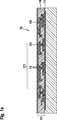
Eine erste Aufbauvariante des erfindungsgemäßen Bauteils erfordert drei Substrate, ein ASIC-Substrat, ein MEMS-Substrat und einen Kappenwafer, und dementsprechend zwei Montageschritte. Die mikromechanische Struktur des MEMS-Bauelements erstreckt sich hier über die gesamte Dicke des MEMS-Substrats. Der Kappenwafer wird über der mikromechanischen Struktur auf dem MEMS-Bauelement oder auf dem ASIC-Bauelement montiert. Diese Aufbauvariante eignet sich insbesondere für Sensoranwendungen. Da sich die Sensorstruktur über die gesamte Dicke des MEMS-Substrats erstreckt, können besonders große seismische Massen auf vergleichsweise kleiner Chipfläche realisiert werden.A first construction variant of the component according to the invention requires three substrates, an ASIC substrate, a MEMS substrate and a cap wafer, and accordingly two assembly steps. The micromechanical structure of the MEMS component here extends over the entire thickness of the MEMS substrate. The cap wafer is mounted over the micromechanical structure on the MEMS device or on the ASIC device. This construction variant is particularly suitable for sensor applications. Since the sensor structure over the extends entire thickness of the MEMS substrate, particularly large seismic masses can be realized on a relatively small chip area.
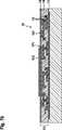
Die zweite Aufbauvariante benötigt lediglich zwei Substrate, ein ASIC-Substrat und ein MEMS-Substrat, die unabhängig voneinander prozessiert werden, und dementsprechend nur einen Montageschritt. Hier wird die mikromechanische Struktur des MEMS-Bauelements in einem Schichtaufbau auf einem Grundsubstrat realisiert, bevor das MEMS-Bauelement face-down auf dem bereits prozessierten ASIC-Substrat montiert wird. In diesem Fall ist die mikromechanische Struktur des MEMS-Bauelements in einem Hohlraum zwischen dem Grundsubstrat des MEMS-Bauelements und dem ASIC-Bauelement angeordnet, so dass das Grundsubstrat des MEMS-Bauelements als Kappe für die mikromechanische Struktur des MEMS-Bauelements fungiert. Mit dieser zweiten Aufbauvariante können Bauteile mit einer vergleichsweise geringen Bauhöhe realisiert werden.The second construction variant requires only two substrates, an ASIC substrate and a MEMS substrate, which are processed independently of one another, and accordingly only one assembly step. Here, the micromechanical structure of the MEMS device is realized in a layer structure on a base substrate before the MEMS device is mounted face-down on the already processed ASIC substrate. In this case, the micromechanical structure of the MEMS device is arranged in a cavity between the base substrate of the MEMS device and the ASIC device, such that the base substrate of the MEMS device functions as a cap for the micromechanical structure of the MEMS device. With this second construction variant components can be realized with a comparatively low overall height.
Kurze Beschreibung der ZeichnungenBrief description of the drawings
Wie bereits voranstehend erörtert, gibt es verschiedene Möglichkeiten, die vorliegende Erfindung in vorteilhafter Weise auszugestalten und weiterzubilden. Dazu wird einerseits auf die den unabhängigen Patentansprüchen nachgeordneten Patentansprüche verwiesen und andererseits auf die nachfolgende Beschreibung zweier Ausführungsbeispiele der Erfindung anhand der Figuren.As already discussed above, there are various possibilities for embodying and developing the present invention in an advantageous manner. For this purpose, reference is made on the one hand to the claims subordinate to the independent claims and on the other hand to the following description of two embodiments of the invention with reference to FIGS.
Ausführungsformen der ErfindungEmbodiments of the invention
Bei beiden beanspruchten und nachfolgend in Verbindung mit den
Erfindungsgemäß wird entweder auf diese Passivierung
Nach der Realisierung der Magnetsensorik auf bzw. im Schichtaufbau des CMOS-Backendstapels
Die strukturierte Oxidschicht
Der erste Strukturierungsschritt dient dem Erzeugen von Durchkontakten, sogenannten Vias
Erst im zweiten Strukturierungsschritt wird die mikromechanische Sensorstruktur
Dann wird ein vorstrukturierter Kappenwafer
Das in
Wie im Fall des Bauteils
Die nachfolgend beschriebene zweite Verfahrensvariante zum Herstellen eines hybrid integrierten Bauteils
Bei dem MEMS-Substrat
In einem nachfolgenden Epitaxieprozess wird eine dicke polykristalline Silizium-Funktionsschicht
Die mikromechanische Struktur
Das so prozessierte MEMS-Substrat
ZITATE ENTHALTEN IN DER BESCHREIBUNG QUOTES INCLUDE IN THE DESCRIPTION
Diese Liste der vom Anmelder aufgeführten Dokumente wurde automatisiert erzeugt und ist ausschließlich zur besseren Information des Lesers aufgenommen. Die Liste ist nicht Bestandteil der deutschen Patent- bzw. Gebrauchsmusteranmeldung. Das DPMA übernimmt keinerlei Haftung für etwaige Fehler oder Auslassungen.This list of the documents listed by the applicant has been generated automatically and is included solely for the better information of the reader. The list is not part of the German patent or utility model application. The DPMA assumes no liability for any errors or omissions.
Zitierte PatentliteraturCited patent literature
- US 2011/0049652 A1[0005, 0005]US 2011/0049652 A1[0005, 0005]
Claims (12)
Translated fromGermanPriority Applications (4)
| Application Number | Priority Date | Filing Date | Title |
|---|---|---|---|
| DE102012210049ADE102012210049A1 (en) | 2012-06-14 | 2012-06-14 | Hybrid integrated component and method for its production |
| US13/916,094US9169116B2 (en) | 2012-06-14 | 2013-06-12 | Hybrid integrated component and method for the manufacture thereof |
| TW102120839ATWI586604B (en) | 2012-06-14 | 2013-06-13 | Hybrid integrated component and process for its production |
| CN201310410451.8ACN103523741B (en) | 2012-06-14 | 2013-06-14 | The parts of hybrid integrated and its manufacture method |
Applications Claiming Priority (1)
| Application Number | Priority Date | Filing Date | Title |
|---|---|---|---|
| DE102012210049ADE102012210049A1 (en) | 2012-06-14 | 2012-06-14 | Hybrid integrated component and method for its production |
Publications (1)
| Publication Number | Publication Date |
|---|---|
| DE102012210049A1true DE102012210049A1 (en) | 2013-12-19 |
Family
ID=49667964
Family Applications (1)
| Application Number | Title | Priority Date | Filing Date |
|---|---|---|---|
| DE102012210049APendingDE102012210049A1 (en) | 2012-06-14 | 2012-06-14 | Hybrid integrated component and method for its production |
Country Status (4)
| Country | Link |
|---|---|
| US (1) | US9169116B2 (en) |
| CN (1) | CN103523741B (en) |
| DE (1) | DE102012210049A1 (en) |
| TW (1) | TWI586604B (en) |
Cited By (1)
| Publication number | Priority date | Publication date | Assignee | Title |
|---|---|---|---|---|
| DE102020204961A1 (en) | 2020-04-20 | 2021-10-21 | Robert Bosch Gesellschaft mit beschränkter Haftung | Method of manufacturing a microelectronic device |
Families Citing this family (30)
| Publication number | Priority date | Publication date | Assignee | Title |
|---|---|---|---|---|
| DE102012206854B4 (en)* | 2012-04-25 | 2020-11-12 | Robert Bosch Gmbh | Hybrid integrated component and process for its manufacture |
| DE102012210049A1 (en)* | 2012-06-14 | 2013-12-19 | Robert Bosch Gmbh | Hybrid integrated component and method for its production |
| DE102012219465A1 (en)* | 2012-10-24 | 2014-04-24 | Robert Bosch Gmbh | Method for producing a cap for a MEMS component and hybrid integrated component with such a cap |
| CN104140072B (en)* | 2013-05-09 | 2016-07-13 | 苏州敏芯微电子技术股份有限公司 | Integrated chip of microelectromechanical system and integrated circuit and manufacturing method thereof |
| US9508663B2 (en)* | 2013-07-24 | 2016-11-29 | Invensense, Inc. | Assembly and packaging of MEMS device |
| TW201508890A (en)* | 2013-08-21 | 2015-03-01 | Richtek Technology Corp | Manufacturing method of micro-electro-mechanical system device and micro-electro-mechanical system device made thereby |
| US9617150B2 (en)* | 2013-10-09 | 2017-04-11 | Taiwan Semiconductor Manufacturing Co., Ltd. | Micro-electro mechanical system (MEMS) device having a blocking layer formed between closed chamber and a dielectric layer of a CMOS substrate |
| US9487391B2 (en) | 2013-11-19 | 2016-11-08 | Taiwan Semiconductor Manufacturing Co., Ltd. | Micro-electro mechanical system (MEMS) device having a blocking layer formed between closed chamber and a dielectric layer of a CMOS substrate |
| US9567206B2 (en)* | 2013-11-19 | 2017-02-14 | Taiwan Semiconductor Manufacturing Co., Ltd. | Structures and formation methods of micro-electro mechanical system device |
| US9725301B2 (en) | 2013-11-19 | 2017-08-08 | Taiwan Semiconductor Manufacturing Co., Ltd. | Structures and formation methods of micro-electro mechanical system device |
| CN103922273B (en)* | 2014-04-30 | 2016-01-13 | 安徽北方芯动联科微系统技术有限公司 | The manufacture method of stack combinations formula MEMS chip and stack combinations formula MEMS chip thereof |
| DE102014210907A1 (en)* | 2014-06-06 | 2015-12-17 | Robert Bosch Gmbh | ASIC component, in particular as a component of a vertically hybrid integrated component |
| US9630834B2 (en)* | 2014-06-16 | 2017-04-25 | InSense, Inc. | Wafer scale monolithic CMOS-integration of free- and non-free-standing Metal- and Metal alloy-based MEMS structures in a sealed cavity |
| CN105428256B (en)* | 2014-07-30 | 2018-07-20 | 中芯国际集成电路制造(上海)有限公司 | A kind of semiconductor devices and its manufacturing method and electronic device |
| CN105366624B (en)* | 2014-07-30 | 2017-06-13 | 中芯国际集成电路制造(上海)有限公司 | A kind of semiconductor devices and its manufacture method and electronic installation |
| US10364143B2 (en)* | 2014-12-18 | 2019-07-30 | Stmicroelectronics S.R.L. | Integrated micro-electromechanical device of semiconductor material having a diaphragm, such as a pressure sensor and an actuator |
| CN106365115B (en)* | 2015-07-23 | 2019-08-23 | 上海丽恒光微电子科技有限公司 | MEMS sensor and preparation method thereof |
| CN105253851B (en)* | 2015-09-14 | 2017-03-22 | 合肥芯福传感器技术有限公司 | Chip-level system sensor and preparation method thereof |
| US20170114630A1 (en)* | 2015-10-22 | 2017-04-27 | MicroPulse, LLC | Integrated measurement while drilling directional controller |
| US10550682B2 (en) | 2015-10-22 | 2020-02-04 | Micropulse, Llc. | Programmable integrated measurement while drilling directional controller |
| US9884758B2 (en) | 2016-01-15 | 2018-02-06 | Taiwan Semiconductor Manufacturing Co., Ltd. | Selective nitride outgassing process for MEMS cavity pressure control |
| GB2546830B (en)* | 2016-01-29 | 2018-11-14 | Cirrus Logic Int Semiconductor Ltd | Integrated MEMS transducers |
| US10160639B2 (en) | 2016-06-27 | 2018-12-25 | Taiwan Semiconductor Manufacturing Co., Ltd. | Semiconductor structure for MEMS Device |
| US10131541B2 (en) | 2016-07-21 | 2018-11-20 | Taiwan Semiconductor Manufacturing Co., Ltd. | MEMS devices having tethering structures |
| WO2018054470A1 (en)* | 2016-09-22 | 2018-03-29 | Robert Bosch Gmbh | Micromechanical component |
| CN207993845U (en)* | 2016-11-10 | 2018-10-19 | 北京万应科技有限公司 | A kind of intelligent sensing modular structure |
| US11193989B2 (en)* | 2018-07-27 | 2021-12-07 | Allegro Microsystems, Llc | Magnetoresistance assembly having a TMR element disposed over or under a GMR element |
| US20210165010A1 (en)* | 2019-11-29 | 2021-06-03 | Seiko Epson Corporation | Sensor unit, electronic apparatus, and moving object |
| CN111470470B (en)* | 2020-06-08 | 2023-03-28 | 宁波中车时代传感技术有限公司 | Preparation method of fluxgate chip |
| CN113213418B (en)* | 2021-04-27 | 2024-03-29 | 西安紫光国芯半导体有限公司 | Micro-electromechanical system chip and electronic equipment |
Citations (1)
| Publication number | Priority date | Publication date | Assignee | Title |
|---|---|---|---|---|
| US20110049652A1 (en) | 2009-08-28 | 2011-03-03 | Miradia Inc. | Method and system for mems devices |
Family Cites Families (31)
| Publication number | Priority date | Publication date | Assignee | Title |
|---|---|---|---|---|
| JP2004264060A (en)* | 2003-02-14 | 2004-09-24 | Akebono Brake Ind Co Ltd | Error correction method in attitude detector, and action measuring instrument using the same |
| TWI390229B (en)* | 2006-03-31 | 2013-03-21 | Citizen Electronics | Magnetic sensor component and magnetic sensor |
| US7456042B2 (en)* | 2006-06-04 | 2008-11-25 | Robert Bosch Gmbh | Microelectromechanical systems having stored charge and methods for fabricating and using same |
| SE534510C2 (en)* | 2008-11-19 | 2011-09-13 | Silex Microsystems Ab | Functional encapsulation |
| WO2010107436A1 (en)* | 2009-03-19 | 2010-09-23 | Hewlett-Packard Development Company, L.P. | Three phase capacitance-based sensing |
| DE102009026628A1 (en)* | 2009-06-02 | 2010-12-09 | Robert Bosch Gmbh | Micromechanical component and method for producing a micromechanical component |
| US8823007B2 (en)* | 2009-10-28 | 2014-09-02 | MCube Inc. | Integrated system on chip using multiple MEMS and CMOS devices |
| US8569092B2 (en)* | 2009-12-28 | 2013-10-29 | General Electric Company | Method for fabricating a microelectromechanical sensor with a piezoresistive type readout |
| US8338208B2 (en)* | 2009-12-31 | 2012-12-25 | Texas Instruments Incorporated | Micro-electro-mechanical system having movable element integrated into leadframe-based package |
| EP2365521B1 (en)* | 2010-01-22 | 2018-12-26 | IMEC vzw | Thin film wafer level package |
| TWI434803B (en)* | 2010-06-30 | 2014-04-21 | Ind Tech Res Inst | Apparatus integrating microelectromechanical system device with circuit chip and methods for fabricating the same |
| US8461656B2 (en)* | 2010-06-30 | 2013-06-11 | Freescale Semiconductor, Inc. | Device structures for in-plane and out-of-plane sensing micro-electro-mechanical systems (MEMS) |
| US8486744B2 (en)* | 2010-09-28 | 2013-07-16 | Taiwan Semiconductor Manufacturing Company, Ltd. | Multiple bonding in wafer level packaging |
| WO2012051340A1 (en)* | 2010-10-12 | 2012-04-19 | Analog Devices, Inc. | Microphone package with embedded asic |
| US8836116B2 (en)* | 2010-10-21 | 2014-09-16 | Taiwan Semiconductor Manufacturing Company, Ltd. | Wafer level packaging of micro-electro-mechanical systems (MEMS) and complementary metal-oxide-semiconductor (CMOS) substrates |
| TWI434802B (en)* | 2010-12-23 | 2014-04-21 | Ind Tech Res Inst | Microelectromechanical device with electric insulating structure and manufacturing method thereof |
| US8232614B1 (en)* | 2011-03-08 | 2012-07-31 | Taiwan Semiconductor Manufacturing Company, Ltd. | Package systems having a conductive element through a substrate thereof and manufacturing methods of the same |
| DE102011005764A1 (en)* | 2011-03-18 | 2012-09-20 | Robert Bosch Gmbh | Apparatus and method for measuring magnetic fields |
| JP6289364B2 (en)* | 2011-06-30 | 2018-03-07 | ムラタ エレクトロニクス オサケユキチュア | Method for manufacturing system-in-package device and system-in-package device |
| US20130127879A1 (en)* | 2011-11-18 | 2013-05-23 | Qualcomm Mems Technologies, Inc. | Glass-encapsulated pressure sensor |
| US8587077B2 (en)* | 2012-01-02 | 2013-11-19 | Windtop Technology Corp. | Integrated compact MEMS device with deep trench contacts |
| JP2013193172A (en)* | 2012-03-21 | 2013-09-30 | Toshiba Corp | Stacked package and method of manufacturing stacked package |
| DE102012206531B4 (en)* | 2012-04-17 | 2015-09-10 | Infineon Technologies Ag | Method for producing a cavity within a semiconductor substrate |
| DE102012206732B4 (en)* | 2012-04-24 | 2024-12-12 | Robert Bosch Gmbh | Method for producing a hybrid integrated component |
| DE102012206875B4 (en)* | 2012-04-25 | 2021-01-28 | Robert Bosch Gmbh | Method for producing a hybrid integrated component and a corresponding hybrid integrated component |
| DE102012210049A1 (en)* | 2012-06-14 | 2013-12-19 | Robert Bosch Gmbh | Hybrid integrated component and method for its production |
| US8729646B2 (en)* | 2012-08-09 | 2014-05-20 | Taiwan Semiconductor Manufacturing Company, Ltd. | MEMS devices and methods for forming the same |
| US10160632B2 (en)* | 2012-08-21 | 2018-12-25 | Robert Bosch Gmbh | System and method for forming a buried lower electrode in conjunction with an encapsulated MEMS device |
| DE102012219465A1 (en)* | 2012-10-24 | 2014-04-24 | Robert Bosch Gmbh | Method for producing a cap for a MEMS component and hybrid integrated component with such a cap |
| DE102012219550B4 (en)* | 2012-10-25 | 2024-04-18 | Robert Bosch Gmbh | Hybrid integrated component |
| DE102013208825B4 (en)* | 2013-05-14 | 2021-05-20 | Robert Bosch Gmbh | Microstructure component and method for manufacturing a microstructure component |
- 2012
- 2012-06-14DEDE102012210049Apatent/DE102012210049A1/enactivePending
- 2013
- 2013-06-12USUS13/916,094patent/US9169116B2/enactiveActive
- 2013-06-13TWTW102120839Apatent/TWI586604B/enactive
- 2013-06-14CNCN201310410451.8Apatent/CN103523741B/enactiveActive
Patent Citations (1)
| Publication number | Priority date | Publication date | Assignee | Title |
|---|---|---|---|---|
| US20110049652A1 (en) | 2009-08-28 | 2011-03-03 | Miradia Inc. | Method and system for mems devices |
Cited By (1)
| Publication number | Priority date | Publication date | Assignee | Title |
|---|---|---|---|---|
| DE102020204961A1 (en) | 2020-04-20 | 2021-10-21 | Robert Bosch Gesellschaft mit beschränkter Haftung | Method of manufacturing a microelectronic device |
Also Published As
| Publication number | Publication date |
|---|---|
| US20130334621A1 (en) | 2013-12-19 |
| TWI586604B (en) | 2017-06-11 |
| CN103523741A (en) | 2014-01-22 |
| US9169116B2 (en) | 2015-10-27 |
| TW201416312A (en) | 2014-05-01 |
| CN103523741B (en) | 2017-01-04 |
Similar Documents
| Publication | Publication Date | Title |
|---|---|---|
| DE102012210049A1 (en) | Hybrid integrated component and method for its production | |
| DE102012208032B4 (en) | Hybrid integrated component with MEMS component and ASIC component | |
| DE102012206854B4 (en) | Hybrid integrated component and process for its manufacture | |
| DE102012206875B4 (en) | Method for producing a hybrid integrated component and a corresponding hybrid integrated component | |
| DE102012208031A1 (en) | + Hybrid integrated component and process for its production | |
| DE602004004513T2 (en) | METHOD FOR PRODUCING AN ELECTRONIC DEVICE AND ELECTRONIC DEVICE | |
| DE102006011545B4 (en) | Micromechanical combination component and corresponding manufacturing method | |
| DE102006022336B4 (en) | Magnetic field sensor and Sensoranordenung with the same | |
| DE102014200512B4 (en) | Micromechanical pressure sensor device and corresponding manufacturing method | |
| DE102012208030B4 (en) | Micromechanical inertial sensor and method for its manufacture | |
| DE102012219550B4 (en) | Hybrid integrated component | |
| DE102012208033A1 (en) | Hybrid integrated component and method for its production | |
| DE102014200507A1 (en) | Micromechanical pressure sensor device and corresponding manufacturing method | |
| DE102012206732A1 (en) | Method for producing a hybrid integrated component | |
| DE102013222733A1 (en) | Micromechanical sensor device | |
| DE102014211333A1 (en) | Micromechanical component and method for its production | |
| DE102016219807B4 (en) | Micromechanical sensor | |
| DE102013104463A1 (en) | A chip packaging package and method of forming a chip packaging package | |
| DE102015217918A1 (en) | Micromechanical component | |
| DE102009026738A1 (en) | Micromechanical acceleration sensor and method for producing an acceleration sensor | |
| DE102006010484A1 (en) | motion sensor | |
| DE102012208053A1 (en) | Hybrid integrated component and method for its production | |
| DE102009045693B4 (en) | Micromechanical component for a Hall sensor device and method for producing a micromechanical component for a Hall sensor device | |
| DE102015217921A1 (en) | Micromechanical component | |
| DE102012219616B4 (en) | Micromechanical component with bond connection |
Legal Events
| Date | Code | Title | Description |
|---|---|---|---|
| R012 | Request for examination validly filed |