DE102012202179A1 - Magnetic field sensor and method for manufacturing a magnetic field sensor - Google Patents
Magnetic field sensor and method for manufacturing a magnetic field sensorDownload PDFInfo
- Publication number
- DE102012202179A1 DE102012202179A1DE102012202179ADE102012202179ADE102012202179A1DE 102012202179 A1DE102012202179 A1DE 102012202179A1DE 102012202179 ADE102012202179 ADE 102012202179ADE 102012202179 ADE102012202179 ADE 102012202179ADE 102012202179 A1DE102012202179 A1DE 102012202179A1
- Authority
- DE
- Germany
- Prior art keywords
- circuit board
- magnetic flux
- area
- flux collector
- magnetic field
- Prior art date
- Legal status (The legal status is an assumption and is not a legal conclusion. Google has not performed a legal analysis and makes no representation as to the accuracy of the status listed.)
- Granted
Links
Images


Classifications
- G—PHYSICS
- G01—MEASURING; TESTING
- G01R—MEASURING ELECTRIC VARIABLES; MEASURING MAGNETIC VARIABLES
- G01R33/00—Arrangements or instruments for measuring magnetic variables
- G01R33/02—Measuring direction or magnitude of magnetic fields or magnetic flux
- G01R33/06—Measuring direction or magnitude of magnetic fields or magnetic flux using galvano-magnetic devices
- G01R33/07—Hall effect devices
- G01R33/072—Constructional adaptation of the sensor to specific applications
- G—PHYSICS
- G01—MEASURING; TESTING
- G01R—MEASURING ELECTRIC VARIABLES; MEASURING MAGNETIC VARIABLES
- G01R33/00—Arrangements or instruments for measuring magnetic variables
- G01R33/0011—Arrangements or instruments for measuring magnetic variables comprising means, e.g. flux concentrators, flux guides, for guiding or concentrating the magnetic flux, e.g. to the magnetic sensor
- H—ELECTRICITY
- H05—ELECTRIC TECHNIQUES NOT OTHERWISE PROVIDED FOR
- H05K—PRINTED CIRCUITS; CASINGS OR CONSTRUCTIONAL DETAILS OF ELECTRIC APPARATUS; MANUFACTURE OF ASSEMBLAGES OF ELECTRICAL COMPONENTS
- H05K1/00—Printed circuits
- H05K1/18—Printed circuits structurally associated with non-printed electric components
- H—ELECTRICITY
- H05—ELECTRIC TECHNIQUES NOT OTHERWISE PROVIDED FOR
- H05K—PRINTED CIRCUITS; CASINGS OR CONSTRUCTIONAL DETAILS OF ELECTRIC APPARATUS; MANUFACTURE OF ASSEMBLAGES OF ELECTRICAL COMPONENTS
- H05K3/00—Apparatus or processes for manufacturing printed circuits
- H05K3/30—Assembling printed circuits with electric components, e.g. with resistor
- H—ELECTRICITY
- H05—ELECTRIC TECHNIQUES NOT OTHERWISE PROVIDED FOR
- H05K—PRINTED CIRCUITS; CASINGS OR CONSTRUCTIONAL DETAILS OF ELECTRIC APPARATUS; MANUFACTURE OF ASSEMBLAGES OF ELECTRICAL COMPONENTS
- H05K2201/00—Indexing scheme relating to printed circuits covered by H05K1/00
- H05K2201/09—Shape and layout
- H05K2201/09009—Substrate related
- H05K2201/09072—Hole or recess under component or special relationship between hole and component
- H—ELECTRICITY
- H05—ELECTRIC TECHNIQUES NOT OTHERWISE PROVIDED FOR
- H05K—PRINTED CIRCUITS; CASINGS OR CONSTRUCTIONAL DETAILS OF ELECTRIC APPARATUS; MANUFACTURE OF ASSEMBLAGES OF ELECTRICAL COMPONENTS
- H05K2201/00—Indexing scheme relating to printed circuits covered by H05K1/00
- H05K2201/10—Details of components or other objects attached to or integrated in a printed circuit board
- H05K2201/10007—Types of components
- H05K2201/10151—Sensor
- H—ELECTRICITY
- H05—ELECTRIC TECHNIQUES NOT OTHERWISE PROVIDED FOR
- H05K—PRINTED CIRCUITS; CASINGS OR CONSTRUCTIONAL DETAILS OF ELECTRIC APPARATUS; MANUFACTURE OF ASSEMBLAGES OF ELECTRICAL COMPONENTS
- H05K2201/00—Indexing scheme relating to printed circuits covered by H05K1/00
- H05K2201/10—Details of components or other objects attached to or integrated in a printed circuit board
- H05K2201/10431—Details of mounted components
- H05K2201/10507—Involving several components
- H05K2201/10545—Related components mounted on both sides of the PCB
- Y—GENERAL TAGGING OF NEW TECHNOLOGICAL DEVELOPMENTS; GENERAL TAGGING OF CROSS-SECTIONAL TECHNOLOGIES SPANNING OVER SEVERAL SECTIONS OF THE IPC; TECHNICAL SUBJECTS COVERED BY FORMER USPC CROSS-REFERENCE ART COLLECTIONS [XRACs] AND DIGESTS
- Y10—TECHNICAL SUBJECTS COVERED BY FORMER USPC
- Y10T—TECHNICAL SUBJECTS COVERED BY FORMER US CLASSIFICATION
- Y10T29/00—Metal working
- Y10T29/49—Method of mechanical manufacture
- Y10T29/49002—Electrical device making
- Y10T29/49117—Conductor or circuit manufacturing
- Y10T29/49124—On flat or curved insulated base, e.g., printed circuit, etc.
- Y10T29/4913—Assembling to base an electrical component, e.g., capacitor, etc.
Landscapes
- Physics & Mathematics (AREA)
- Engineering & Computer Science (AREA)
- Condensed Matter Physics & Semiconductors (AREA)
- General Physics & Mathematics (AREA)
- Microelectronics & Electronic Packaging (AREA)
- Manufacturing & Machinery (AREA)
- Measuring Magnetic Variables (AREA)
- Hall/Mr Elements (AREA)
- Measuring Instrument Details And Bridges, And Automatic Balancing Devices (AREA)
Abstract
Translated fromGerman
Description
Translated fromGermanDie Erfindung betrifft einen Magnetfeldsensor und ein Verfahren zum Herstellen eines Magnetfeldsensors, insbesondere bei der Bestückung von Hallsensoren in SMD-Gehäusen mit Magnetflusssammlern.The invention relates to a magnetic field sensor and a method for producing a magnetic field sensor, in particular in the assembly of Hall sensors in SMD housings with magnetic flux collector.
Stand der TechnikState of the art
In vielen Anwendungen ist es notwendig oder wünschenswert, das Magnetfeld der Umgebung zu messen. Dabei können unterschiedliche Sensoren eingesetzt werden. Häufig werden Hallsensoren eingesetzt, die auf der Basis des Hall-Effekts einer von einem magnetischen Fluss durchsetzten Leiterschleife eine elektrische Spannung bzw. einen elektrischen Strom als Ausgangssignal erzeugen. Diese Hallsensoren können für die Großserienfertigung in oberflächenmontierten Gehäusen (SMD-Gehäuse, „surface mounted devices“) gehäust sein. Insbesondere können mehrere Hallsensoren innerhalb eines Gehäuses integriert sein, beispielsweise für differentielle Magnetfeldmessungen.In many applications it is necessary or desirable to measure the magnetic field of the environment. Different sensors can be used. Frequently, Hall sensors are used which generate an electrical voltage or an electric current as an output signal on the basis of the Hall effect of a conductor loop penetrated by a magnetic flux. These Hall sensors can be housed in surface mount housings (SMD housings, "surface mounted devices") for mass production. In particular, a plurality of Hall sensors may be integrated within a housing, for example for differential magnetic field measurements.
Mit Hallsensoren können betragsmäßig sehr kleine Magnetfelder gemessen werden. Dazu kann es vorteilhaft sein, den magnetischen Fluss über eine bestimmte Fläche zu sammeln und durch die aktive Fläche des Hallsensors zu leiten. Damit kann eine Verstärkung des Magnetfelds über die aktive Fläche des Hallsensors erreicht werden.With Hall sensors, very small magnetic fields can be measured in terms of amount. For this purpose, it may be advantageous to collect the magnetic flux over a certain area and to guide it through the active area of the Hall sensor. Thus, an amplification of the magnetic field over the active surface of the Hall sensor can be achieved.
In der Druckschrift
Es besteht daher ein Bedarf an Magnetfeldsensoren, mit welchen ein magnetischer Fluss über der aktiven Fläche des darin integrierten Hallsensors gebündelt werden kann. Dabei ist insbesondere eine kostengünstige Realisierung erwünscht, die mit geringem Zusatzaufwand in einer Großserienfertigung in der Fertigung der Magnetfeldsensoren implementiert werden kann.There is therefore a need for magnetic field sensors with which a magnetic flux can be bundled over the active surface of the integrated Hall sensor. In particular, a cost-effective implementation is desired, which can be implemented with little additional effort in a large-scale production in the production of magnetic field sensors.
Offenbarung der ErfindungDisclosure of the invention
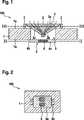
Die vorliegende Erfindung schafft gemäß einem Aspekt einen Magnetfeldsensor, mit einer Leiterplatte mit einer ersten Oberfläche, einer der ersten Oberfläche gegenüberliegenden zweiten Oberfläche und einer sich von der ersten Oberfläche zur zweiten Oberfläche erstreckenden Aussparung, einem Hallsensorbauelement, welches ein Gehäuse und mindestens einen in dem Gehäuse angeordneten Hallsensor mit einer parallel zu der ersten Oberfläche angeordneten aktiven Sensorfläche aufweist, und welches in dem Bereich der Aussparung auf der Seite der zweiten Oberfläche auf der Leiterplatte angeordnet ist, und einen ersten Magnetflusssammler aus einem magnetisch permeablen Material, welcher auf der Seite der ersten Oberfläche auf der Leiterplatte gegenüberliegend des Hallsensorbauelements angeordnet ist, und welcher eine von der Leiterplatte abgewandte Seitenfläche mit einem ersten Flächeninhalt und eine der Leiterplatte zugewandte Seitenfläche mit einem zweiten Flächeninhalt aufweist, wobei der erste Flächeninhalt größer als der zweite Flächeninhalt ist.The present invention, in one aspect, provides a magnetic field sensor comprising a circuit board having a first surface, a second surface opposite the first surface, and a recess extending from the first surface to the second surface, a Hall sensor device having a housing and at least one in the housing arranged Hall sensor having a parallel to the first surface arranged active sensor surface, and which is arranged in the region of the recess on the side of the second surface on the circuit board, and a first magnetic flux collector of a magnetically permeable material, which on the side of the first surface is arranged on the circuit board opposite the Hall sensor component, and which has a side facing away from the circuit board side surface with a first surface area and a side facing the printed circuit board with a second surface area t, wherein the first area is greater than the second area.
Die vorliegende Erfindung schafft gemäß einem weiteren Aspekt ein Verfahren zum Herstellen eines Magnetfeldsensors, mit den Schritten des Montierens eines Hallsensorbauelements, welches ein Gehäuse und mindestens einen in dem Gehäuse angeordneten Hallsensor aufweist, auf einer Leiterplatte mit einer ersten Oberfläche, einer der ersten Oberfläche gegenüberliegenden zweiten Oberfläche und einer sich von der ersten Oberfläche zur zweiten Oberfläche erstreckenden Aussparung in dem Bereich der Aussparung auf der Seite der zweiten Oberfläche, und des Montierens eines ersten Magnetflusssammlers aus einem magnetisch permeablen Material auf der Seite der ersten Oberfläche auf der Leiterplatte gegenüberliegend des Hallsensorbauelements, wobei der Magnetflusssammler eine von der Leiterplatte abgewandte Seitenfläche mit einem ersten Flächeninhalt und eine der Leiterplatte zugewandte Seitenfläche mit einem zweiten Flächeninhalt aufweist, und wobei der erste Flächeninhalt größer als der zweite Flächeninhalt ist.The present invention according to another aspect provides a method of manufacturing a magnetic field sensor, comprising the steps of mounting a Hall sensor device having a housing and at least one Hall sensor disposed in the housing on a circuit board having a first surface, a second surface opposite the first surface A surface and a recess extending from the first surface to the second surface in the region of the recess on the side of the second surface, and mounting a first magnetic flux collector of a magnetically permeable material on the side of the first surface on the circuit board opposite the Hall sensor device, wherein the magnetic flux collector has a side surface facing away from the printed circuit board with a first surface area and a side surface facing the printed circuit board with a second surface area, and wherein the first surface area is larger than the second area is.
Vorteile der ErfindungAdvantages of the invention
Es ist eine Idee der vorliegenden Erfindung, einen Magnetflusssammler für einen Hallsensor bereitzustellen, der in SMD-Technologie auf einer Leiterplatte bestückt werden kann. Der Magnetflusssammler verstärkt das Magnetfeld über einer aktiven Fläche eines Hallsensors. Insbesondere wird mit diesem Magnetflusssammler eine Integration in eine Großserienfertigungslinie möglich, ohne dass eine aufwändige Integration des Magnetflusssammlers in die Konstruktion des Hallsensors notwendig wird.It is an idea of the present invention to provide a magnetic flux collector for a Hall sensor that can be populated in SMD technology on a printed circuit board. The magnetic flux collector amplifies the magnetic field over an active area of a Hall sensor. In particular, with this magnetic flux collector integration into a mass production line is possible without a complex integration of the magnetic flux collector is necessary in the construction of the Hall sensor.
Ein erheblicher Vorteil dieses Magnetfeldsensors besteht darin, dass die in dem Magnetfeldsensor verwendeten Hallsensoren eine höhere Auflösung sowie ein verbessertes Signal-zu-Rausch-Verhältnis erzielen können. Zugleich kann die elektromagnetische Verträglichkeit (EMV) des Magnetfeldsensors verbessert werden, wenn der Magnetflusssammler mit dem Massepotential des Magnetfeldsensors verbunden wird.A significant advantage of this magnetic field sensor is that the Hall sensors used in the magnetic field sensor can achieve a higher resolution and an improved signal-to-noise ratio. At the same time, the electromagnetic compatibility (EMC) of the Magnetic field sensor can be improved when the magnetic flux collector is connected to the ground potential of the magnetic field sensor.
Gemäß einer Ausführungsform des erfindungsgemäßen Magnetfeldsensors kann der erste Magnetflusssammler eine trapezoide Querschnittsfläche aufweisen. Gemäß einer alternativen Ausführungsform des erfindungsgemäßen Magnetfeldsensors kann der erste Magnetflusssammler eine Querschnittsfläche aufweisen, die einem Längsschnitt durch eine Hälfte eines einschaligen Hyperboloids entspricht. Diese Formen ermöglichen ein effektives Bündeln des magnetischen Flusses über der aktiven Sensorfläche des Hallsensors, insbesondere da der erste Magnetflusssammler mit den angegebenen Formen in die Aussparung hineinreichen kann. Dadurch ergibt sich der Vorteil, dass die Bauform des Magnetfeldsensors insgesamt flach bleibt, ohne dass die Effizienz des Bündelns des magnetischen Flusses beeinträchtigt wird.According to one embodiment of the magnetic field sensor according to the invention, the first magnetic flux collector may have a trapezoidal cross-sectional area. According to an alternative embodiment of the magnetic field sensor according to the invention, the first magnetic flux collector may have a cross-sectional area corresponding to a longitudinal section through one half of a single-sheet hyperboloid. These shapes allow for effective bundling of the magnetic flux across the active sensor surface of the Hall sensor, particularly as the first magnetic flux collector with the indicated shapes can extend into the recess. This has the advantage that the design of the magnetic field sensor remains flat overall, without affecting the efficiency of the bundling of the magnetic flux.
Gemäß einer weiteren Ausführungsform des erfindungsgemäßen Magnetfeldsensors kann der zweite Flächeninhalt der der Leiterplatte zugewandten Seitenfläche des ersten Magnetflusssammlers dem Flächeninhalt der aktiven Sensorfläche des Hallsensors entsprechen. Damit ist eine effektive Verstärkung des Magnetfelds über dem Hallsensor möglich.According to a further embodiment of the magnetic field sensor according to the invention, the second surface area of the side surface of the first magnetic flux collector facing the printed circuit board can correspond to the surface area of the active sensor surface of the Hall sensor. Thus, an effective amplification of the magnetic field over the Hall sensor is possible.
Gemäß einer weiteren Ausführungsform des erfindungsgemäßen Magnetfeldsensors kann das Hallsensorbauelement mindestens zwei entlang der zweiten Oberfläche der Leiterplatte benachbart gelegene Hallsensoren aufweisen, und die der Leiterplatte zugewandte Seitenfläche des ersten Magnetflusssammlers kann über der aktiven Sensorfläche eines der beiden Hallsensoren angeordnet sein. Diese Aufbauform ermöglicht in vorteilhafter Weise eine differentielle Auswertung der Ausgangssignale der beiden Hallsensoren.According to a further embodiment of the magnetic field sensor according to the invention, the Hall sensor component may have at least two Hall sensors adjacent to the second surface of the printed circuit board, and the lateral surface of the first magnetic flux collector facing the printed circuit board may be disposed over the active sensor surface of one of the two Hall sensors. This design allows advantageously a differential evaluation of the output signals of the two Hall sensors.
Gemäß einer weiteren Ausführungsform des erfindungsgemäßen Magnetfeldsensors kann der erste Magnetflusssammler auf der ersten Oberfläche der Leiterplatte mit Lötkontakten befestigt sein. Dies bietet den Vorteil, dass die Montage des Magnetfeldsammlers einfach und kostengünstig in den Bestückungsprozess der Leiterplatten eingebunden werden kann.According to a further embodiment of the magnetic field sensor according to the invention, the first magnetic flux collector may be fastened on the first surface of the printed circuit board with solder contacts. This offers the advantage that the assembly of the magnetic field collector can be easily and inexpensively integrated into the assembly process of the printed circuit boards.
Gemäß einer weiteren Ausführungsform des erfindungsgemäßen Magnetfeldsensors kann der Magnetfeldsensor weiterhin einen zweiten Magnetflusssammler aus einem magnetisch permeablen Material umfassen, welcher auf der Seite der zweiten Oberfläche auf der Leiterplatte so angeordnet ist, dass das Hallsensorbauelement entlang der Erstreckung der Aussparung zwischen dem ersten Magnetflusssammler und dem zweiten Magnetflusssammler angeordnet ist, wobei der zweite Magnetflusssammler eine von der Leiterplatte abgewandte Seitenfläche mit einem dritten Flächeninhalt und eine der Leiterplatte zugewandte Seitenfläche mit einem vierten Flächeninhalt aufweist, und wobei der dritte Flächeninhalt größer als der vierte Flächeninhalt ist. Dadurch ist eine weitergehende Optimierung des magnetischen Flusses durch den bzw. Hallsensoren möglich.According to a further embodiment of the magnetic field sensor according to the invention, the magnetic field sensor may further comprise a second magnetic flux collector made of a magnetically permeable material, which is arranged on the side of the second surface on the circuit board, that the Hall sensor device along the extension of the recess between the first magnetic flux collector and the second Magnetic flux collector is arranged, wherein the second magnetic flux collector has a side facing away from the circuit board side surface with a third surface and a printed circuit board facing side surface having a fourth surface area, and wherein the third surface area is greater than the fourth surface area. As a result, further optimization of the magnetic flux through or Hall sensors is possible.
Gemäß einer Ausführungsform des erfindungsgemäßen Verfahrens kann das Verfahren weiterhin den Schritt des Montierens eines zweiten Magnetflusssammlers aus einem magnetisch permeablen Material auf der Seite der zweiten Oberfläche auf der Leiterplatte umfassen, so dass das Hallsensorbauelement entlang der Erstreckung der Aussparung zwischen dem ersten Magnetflusssammler und dem zweiten Magnetflusssammler angeordnet ist, wobei der zweite Magnetflusssammler eine von der Leiterplatte abgewandte Seitenfläche mit einem dritten Flächeninhalt und eine der Leiterplatte zugewandte Seitenfläche mit einem vierten Flächeninhalt aufweist, und wobei der dritte Flächeninhalt größer als der vierte Flächeninhalt ist.According to an embodiment of the method according to the invention, the method may further comprise the step of mounting a second magnetic flux collector of a magnetically permeable material on the second surface side of the circuit board such that the Hall sensor device extends along the extent of the recess between the first magnetic flux collector and the second magnetic flux collector wherein the second magnetic flux collector has a side surface facing away from the printed circuit board with a third surface area and a side surface facing the printed circuit board with a fourth surface area, and wherein the third surface area is greater than the fourth surface area.
Weitere Merkmale und Vorteile von Ausführungsformen der Erfindung ergeben sich aus der nachfolgenden Beschreibung mit Bezug auf die beigefügten Zeichnungen.Further features and advantages of embodiments of the invention will become apparent from the following description with reference to the accompanying drawings.
Kurze Beschreibung der ZeichnungenBrief description of the drawings
Die beschriebenen Ausgestaltungen und Weiterbildungen lassen sich, sofern sinnvoll, beliebig miteinander kombinieren. Weitere mögliche Ausgestaltungen, Weiterbildungen und Implementierungen der Erfindung umfassen auch nicht explizit genannte Kombinationen von zuvor oder im Folgenden bezüglich der Ausführungsbeispiele beschriebenen Merkmale der Erfindung.The described embodiments and developments can, if appropriate, combine with one another as desired. Further possible refinements, developments and implementations of the invention also include combinations, not explicitly mentioned, of features of the invention described above or below with regard to the exemplary embodiments.
Die beiliegenden Zeichnungen sollen ein weiteres Verständnis der Ausführungsformen der Erfindung vermitteln. Sie veranschaulichen Ausführungsformen und dienen im Zusammenhang mit der Beschreibung der Erklärung von Prinzipien und Konzepten der Erfindung. Andere Ausführungsformen und viele der genannten Vorteile ergeben sich im Hinblick auf die Zeichnungen. Die Elemente der Zeichnungen sind nicht notwendigerweise maßstabsgetreu zueinander gezeigt.The accompanying drawings are intended to provide further understanding of the embodiments of the invention. They illustrate embodiments and, together with the description, serve to explain principles and concepts of the invention. Other embodiments and many of the stated advantages will become apparent with reference to the drawings. The elements of the drawings are not necessarily shown to scale to each other.
Es zeigen:Show it:
Die Leiterplatte
Die Leiterplatte
Das Hallsensorbauelement
Der Magnetflusssammler
Der Magnetflusssammler
Der zweite Flächeninhalt der der Leiterplatte
In
Das Hallsensorbauelement
Die Anzahl der Hallsensoren
Der zweite Magnetflusssammler
Die Anordnung des Hallsensorbauelements
Der zweite Magnetflusssammler
In einem zweiten Schritt
Optional kann in einem dritten Schritt
Die Schritte
Die vorstehend erläuterten Magnetfeldsensoren und deren Herstellungsverfahren können beispielsweise in allen Anwendungen eingesetzt werden, in denen ein Magnetfeld räumlich aufgelöst erfasst werden soll. Besonders vorteilhaft sind diese Magnetfeldsensoren in Anwendungsfällen, in denen Magnetfelder mit geringem Betrag ermittelt werden sollen, beispielsweise in Drehmomentsensoren – zum Beispiel für elektrische Servolenkungen –, drahtlosen Drehmomentsensoren, Stromsensoren, Lageerkennungssensoren, Kompassanwendungen, für kontaktlose Signalgeber oder in ähnlichen Fällen.The above-described magnetic field sensors and their manufacturing methods can be used for example in all applications in which a magnetic field is to be detected spatially resolved. These magnetic field sensors are particularly advantageous in applications in which magnetic fields are to be determined with a small amount, for example in torque sensors - for example for electric power steering systems - wireless torque sensors, current sensors, position detection sensors, compass applications, for contactless signalers or in similar cases.
ZITATE ENTHALTEN IN DER BESCHREIBUNG QUOTES INCLUDE IN THE DESCRIPTION
Diese Liste der vom Anmelder aufgeführten Dokumente wurde automatisiert erzeugt und ist ausschließlich zur besseren Information des Lesers aufgenommen. Die Liste ist nicht Bestandteil der deutschen Patent- bzw. Gebrauchsmusteranmeldung. Das DPMA übernimmt keinerlei Haftung für etwaige Fehler oder Auslassungen.This list of the documents listed by the applicant has been generated automatically and is included solely for the better information of the reader. The list is not part of the German patent or utility model application. The DPMA assumes no liability for any errors or omissions.
Zitierte PatentliteraturCited patent literature
- US 5883567 A[0004]US 5883567 A[0004]
- US 7358724 B2[0004]US 7358724 B2[0004]
Claims (9)
Translated fromGermanPriority Applications (2)
| Application Number | Priority Date | Filing Date | Title |
|---|---|---|---|
| DE102012202179.5ADE102012202179B4 (en) | 2012-02-14 | 2012-02-14 | Magnetic field sensor and method for producing a magnetic field sensor |
| US13/765,381US9024630B2 (en) | 2012-02-14 | 2013-02-12 | Magnetic field sensor and method for manufacturing a magnetic field sensor |
Applications Claiming Priority (1)
| Application Number | Priority Date | Filing Date | Title |
|---|---|---|---|
| DE102012202179.5ADE102012202179B4 (en) | 2012-02-14 | 2012-02-14 | Magnetic field sensor and method for producing a magnetic field sensor |
Publications (2)
| Publication Number | Publication Date |
|---|---|
| DE102012202179A1true DE102012202179A1 (en) | 2013-08-14 |
| DE102012202179B4 DE102012202179B4 (en) | 2021-09-23 |
Family
ID=48868363
Family Applications (1)
| Application Number | Title | Priority Date | Filing Date |
|---|---|---|---|
| DE102012202179.5AExpired - Fee RelatedDE102012202179B4 (en) | 2012-02-14 | 2012-02-14 | Magnetic field sensor and method for producing a magnetic field sensor |
Country Status (2)
| Country | Link |
|---|---|
| US (1) | US9024630B2 (en) |
| DE (1) | DE102012202179B4 (en) |
Families Citing this family (6)
| Publication number | Priority date | Publication date | Assignee | Title |
|---|---|---|---|---|
| CN103412269B (en)* | 2013-07-30 | 2016-01-20 | 江苏多维科技有限公司 | Single-chip push-pull bridge type magnetic field sensor |
| EP2963435B1 (en)* | 2014-07-01 | 2017-01-25 | Nxp B.V. | Differential lateral magnetic field sensor system with offset cancelling and implemented using silicon-on-insulator technology |
| US10168391B2 (en)* | 2015-06-23 | 2019-01-01 | Infineon Technologies Ag | Multi-functional interconnect module and carrier with multi-functional interconnect module attached thereto |
| EP3742182B1 (en)* | 2019-05-24 | 2023-06-28 | Melexis Technologies SA | Semiconductor device with embedded magnetic flux concentrator |
| EP4484987A1 (en)* | 2023-06-28 | 2025-01-01 | Melexis Technologies SA | Magnetic sensor structure, device and system |
| CN118884013B (en)* | 2024-09-27 | 2024-12-31 | 苏州矩阵光电有限公司 | Hall current sensor and preparation method thereof |
Citations (2)
| Publication number | Priority date | Publication date | Assignee | Title |
|---|---|---|---|---|
| US5883567A (en) | 1997-10-10 | 1999-03-16 | Analog Devices, Inc. | Packaged integrated circuit with magnetic flux concentrator |
| US7358724B2 (en) | 2005-05-16 | 2008-04-15 | Allegro Microsystems, Inc. | Integrated magnetic flux concentrator |
Family Cites Families (7)
| Publication number | Priority date | Publication date | Assignee | Title |
|---|---|---|---|---|
| DE2918329A1 (en) | 1979-05-07 | 1980-12-04 | Papst Motoren Kg | METHOD FOR FASTENING A GALVANOMAGNETIC SENSOR IN A RECORD OF A CIRCUIT BOARD |
| US4893073A (en) | 1989-01-30 | 1990-01-09 | General Motors Corporation | Electric circuit board current sensor |
| US6501268B1 (en)* | 2000-08-18 | 2002-12-31 | The United States Of America As Represented By The Secretary Of The Army | Magnetic sensor with modulating flux concentrator for 1/f noise reduction |
| EP1811311B1 (en)* | 2006-01-19 | 2016-08-31 | Melexis Technologies NV | Device for measuring current |
| US7936164B2 (en)* | 2008-07-03 | 2011-05-03 | Allegro Microsystems, Inc. | Folding current sensor |
| US20100188078A1 (en)* | 2009-01-28 | 2010-07-29 | Andrea Foletto | Magnetic sensor with concentrator for increased sensing range |
| US20100271018A1 (en)* | 2009-04-24 | 2010-10-28 | Seagate Technology Llc | Sensors for minute magnetic fields |
- 2012
- 2012-02-14DEDE102012202179.5Apatent/DE102012202179B4/ennot_activeExpired - Fee Related
- 2013
- 2013-02-12USUS13/765,381patent/US9024630B2/enactiveActive
Patent Citations (2)
| Publication number | Priority date | Publication date | Assignee | Title |
|---|---|---|---|---|
| US5883567A (en) | 1997-10-10 | 1999-03-16 | Analog Devices, Inc. | Packaged integrated circuit with magnetic flux concentrator |
| US7358724B2 (en) | 2005-05-16 | 2008-04-15 | Allegro Microsystems, Inc. | Integrated magnetic flux concentrator |
Also Published As
| Publication number | Publication date |
|---|---|
| DE102012202179B4 (en) | 2021-09-23 |
| US20130207650A1 (en) | 2013-08-15 |
| US9024630B2 (en) | 2015-05-05 |
Similar Documents
| Publication | Publication Date | Title |
|---|---|---|
| EP2530475B1 (en) | Device for measuring a current flowing through a cable | |
| EP2867684B1 (en) | Arrangement for measuring current | |
| DE102012202179B4 (en) | Magnetic field sensor and method for producing a magnetic field sensor | |
| DE102007003830B4 (en) | Device for measuring an electrical current flowing through an electrical conductor | |
| DE112016002481T5 (en) | current sensor | |
| EP1772737A2 (en) | Assembly group for the current measurement | |
| DE112009000933T5 (en) | Inductive linear position sensor | |
| DE102008034577B4 (en) | Current measuring arrangement | |
| DE102018211564A1 (en) | Magnetically permeable element and current sensing element | |
| WO2009019200A1 (en) | Arrangement for measuring a current flowing through an electrical conductor | |
| DE102005028572B4 (en) | Current sensor arrangement with a magnetic core | |
| EP3245480B1 (en) | Inductive position determination | |
| DE19800444B4 (en) | Magnetic detection device | |
| EP0886147A1 (en) | Device for obtaining a current-proportional magnetic induction at the position of a magnetic field sensor | |
| DE102019124391B4 (en) | Magnetic field-based current sensor for frequency-compensated measurement of alternating currents | |
| DE102020111626A1 (en) | MAGNETIC SENSOR DEVICE AND METHOD OF MANUFACTURING THE SAME | |
| DE102009049639A1 (en) | Circuit arrangement i.e. surface mounted component, for use in magnetic camera for determining direction and magnitude of magnetic field vector, has carrier including connecting contacts on which arrangement is connected to external device | |
| DE102017202835B4 (en) | Sensor element and sensor device | |
| DE202013010178U1 (en) | Current detection device | |
| EP1327891B1 (en) | Device for measuring a magnetic field, magnetic field sensor and current sensor | |
| DE102014112299B4 (en) | Current sensor and circuit arrangement with a converter and a current sensor | |
| DE102017202592A1 (en) | Control electronics with a magnetic flux guide element | |
| DE102011079050A1 (en) | Method for populating a printed circuit board | |
| DE102023128106A1 (en) | Hybrid throttle device, method for producing such a hybrid throttle device and use of a current measuring sensor element and use of a web-shaped internal component | |
| DE102020200619A1 (en) | Magnetic core of an electronic assembly |
Legal Events
| Date | Code | Title | Description |
|---|---|---|---|
| R012 | Request for examination validly filed | ||
| R016 | Response to examination communication | ||
| R018 | Grant decision by examination section/examining division | ||
| R020 | Patent grant now final | ||
| R079 | Amendment of ipc main class | Free format text:PREVIOUS MAIN CLASS: H01L0043040000 Ipc:H10N0052800000 | |
| R119 | Application deemed withdrawn, or ip right lapsed, due to non-payment of renewal fee |