DE102012201953A1 - Method and device for passivation of solar cells with an aluminum oxide layer - Google Patents
Method and device for passivation of solar cells with an aluminum oxide layerDownload PDFInfo
- Publication number
- DE102012201953A1 DE102012201953A1DE102012201953ADE102012201953ADE102012201953A1DE 102012201953 A1DE102012201953 A1DE 102012201953A1DE 102012201953 ADE102012201953 ADE 102012201953ADE 102012201953 ADE102012201953 ADE 102012201953ADE 102012201953 A1DE102012201953 A1DE 102012201953A1
- Authority
- DE
- Germany
- Prior art keywords
- substrate
- icp
- source
- reaction chamber
- plasma
- Prior art date
- Legal status (The legal status is an assumption and is not a legal conclusion. Google has not performed a legal analysis and makes no representation as to the accuracy of the status listed.)
- Ceased
Links
- 238000000034methodMethods0.000titleclaimsabstractdescription52
- 238000002161passivationMethods0.000titleclaimsdescription11
- TWNQGVIAIRXVLR-UHFFFAOYSA-Noxo(oxoalumanyloxy)alumaneChemical compoundO=[Al]O[Al]=OTWNQGVIAIRXVLR-UHFFFAOYSA-N0.000titledescription10
- 239000000758substrateSubstances0.000claimsabstractdescription55
- 238000009616inductively coupled plasmaMethods0.000claimsabstractdescription54
- 238000006243chemical reactionMethods0.000claimsabstractdescription41
- 238000000576coating methodMethods0.000claimsabstractdescription38
- 239000011248coating agentSubstances0.000claimsabstractdescription37
- 239000007789gasSubstances0.000claimsabstractdescription23
- JLTRXTDYQLMHGR-UHFFFAOYSA-NtrimethylaluminiumChemical compoundC[Al](C)CJLTRXTDYQLMHGR-UHFFFAOYSA-N0.000claimsabstractdescription12
- 229910052782aluminiumInorganic materials0.000claimsabstractdescription10
- -1aluminum compoundChemical class0.000claimsabstractdescription8
- QVGXLLKOCUKJST-UHFFFAOYSA-Natomic oxygenChemical compound[O]QVGXLLKOCUKJST-UHFFFAOYSA-N0.000claimsabstractdescription7
- 238000000151depositionMethods0.000claimsabstractdescription7
- 239000001301oxygenSubstances0.000claimsabstractdescription7
- 229910052760oxygenInorganic materials0.000claimsabstractdescription7
- 150000002927oxygen compoundsChemical class0.000claimsabstractdescription4
- 229910018072Al 2 O 3Inorganic materials0.000claimsabstractdescription3
- 230000008569processEffects0.000claimsdescription21
- 150000002500ionsChemical class0.000claimsdescription17
- 238000005192partitionMethods0.000claimsdescription5
- IJGRMHOSHXDMSA-UHFFFAOYSA-NAtomic nitrogenChemical compoundN#NIJGRMHOSHXDMSA-UHFFFAOYSA-N0.000claimsdescription4
- 230000008878couplingEffects0.000claimsdescription4
- 238000010168coupling processMethods0.000claimsdescription4
- 238000005859coupling reactionMethods0.000claimsdescription4
- 150000003377silicon compoundsChemical class0.000claimsdescription4
- 230000001939inductive effectEffects0.000claimsdescription3
- 229910052710siliconInorganic materials0.000claimsdescription3
- 239000010703siliconSubstances0.000claimsdescription3
- 229910052757nitrogenInorganic materials0.000claimsdescription2
- 229910017464nitrogen compoundInorganic materials0.000claimsdescription2
- 150000002830nitrogen compoundsChemical class0.000claimsdescription2
- 229910017107AlOxInorganic materials0.000abstract2
- 239000000411inducerSubstances0.000abstract1
- 238000004519manufacturing processMethods0.000description8
- 238000000623plasma-assisted chemical vapour depositionMethods0.000description5
- 229910052581Si3N4Inorganic materials0.000description4
- XAGFODPZIPBFFR-UHFFFAOYSA-NaluminiumChemical compound[Al]XAGFODPZIPBFFR-UHFFFAOYSA-N0.000description4
- 238000009434installationMethods0.000description4
- 239000000463materialSubstances0.000description4
- 239000002243precursorSubstances0.000description4
- 239000004065semiconductorSubstances0.000description4
- HQVNEWCFYHHQES-UHFFFAOYSA-Nsilicon nitrideChemical compoundN12[Si]34N5[Si]62N3[Si]51N64HQVNEWCFYHHQES-UHFFFAOYSA-N0.000description4
- 238000000231atomic layer depositionMethods0.000description3
- 230000007723transport mechanismEffects0.000description3
- VYPSYNLAJGMNEJ-UHFFFAOYSA-NSilicium dioxideChemical compoundO=[Si]=OVYPSYNLAJGMNEJ-UHFFFAOYSA-N0.000description2
- XUIMIQQOPSSXEZ-UHFFFAOYSA-NSiliconChemical group[Si]XUIMIQQOPSSXEZ-UHFFFAOYSA-N0.000description2
- 230000008901benefitEffects0.000description2
- 229910021419crystalline siliconInorganic materials0.000description2
- 238000010494dissociation reactionMethods0.000description2
- 230000005593dissociationsEffects0.000description2
- 239000012530fluidSubstances0.000description2
- HBMJWWWQQXIZIP-UHFFFAOYSA-Nsilicon carbideChemical compound[Si+]#[C-]HBMJWWWQQXIZIP-UHFFFAOYSA-N0.000description2
- 229910010271silicon carbideInorganic materials0.000description2
- 229910052814silicon oxideInorganic materials0.000description2
- BUHVIAUBTBOHAG-FOYDDCNASA-N(2r,3r,4s,5r)-2-[6-[[2-(3,5-dimethoxyphenyl)-2-(2-methylphenyl)ethyl]amino]purin-9-yl]-5-(hydroxymethyl)oxolane-3,4-diolChemical compoundCOC1=CC(OC)=CC(C(CNC=2C=3N=CN(C=3N=CN=2)[C@H]2[C@@H]([C@H](O)[C@@H](CO)O2)O)C=2C(=CC=CC=2)C)=C1BUHVIAUBTBOHAG-FOYDDCNASA-N0.000description1
- MYMOFIZGZYHOMD-UHFFFAOYSA-NDioxygenChemical compoundO=OMYMOFIZGZYHOMD-UHFFFAOYSA-N0.000description1
- PNEYBMLMFCGWSK-UHFFFAOYSA-Naluminium oxideInorganic materials[O-2].[O-2].[O-2].[Al+3].[Al+3]PNEYBMLMFCGWSK-UHFFFAOYSA-N0.000description1
- 230000015556catabolic processEffects0.000description1
- 239000007795chemical reaction productSubstances0.000description1
- 150000001875compoundsChemical class0.000description1
- 230000007547defectEffects0.000description1
- 238000006731degradation reactionMethods0.000description1
- 229910001882dioxygenInorganic materials0.000description1
- 238000007599dischargingMethods0.000description1
- 238000009826distributionMethods0.000description1
- 238000010438heat treatmentMethods0.000description1
- 150000002430hydrocarbonsChemical class0.000description1
- 230000000977initiatory effectEffects0.000description1
- 229910003465moissaniteInorganic materials0.000description1
- 230000007935neutral effectEffects0.000description1
- QJGQUHMNIGDVPM-UHFFFAOYSA-Nnitrogen groupChemical group[N]QJGQUHMNIGDVPM-UHFFFAOYSA-N0.000description1
- 239000000376reactantSubstances0.000description1
- 230000009257reactivityEffects0.000description1
- 238000005215recombinationMethods0.000description1
- 230000006798recombinationEffects0.000description1
- 239000000126substanceSubstances0.000description1
- 230000007306turnoverEffects0.000description1
- 238000007740vapor depositionMethods0.000description1
Images

Classifications
- C—CHEMISTRY; METALLURGY
- C23—COATING METALLIC MATERIAL; COATING MATERIAL WITH METALLIC MATERIAL; CHEMICAL SURFACE TREATMENT; DIFFUSION TREATMENT OF METALLIC MATERIAL; COATING BY VACUUM EVAPORATION, BY SPUTTERING, BY ION IMPLANTATION OR BY CHEMICAL VAPOUR DEPOSITION, IN GENERAL; INHIBITING CORROSION OF METALLIC MATERIAL OR INCRUSTATION IN GENERAL
- C23C—COATING METALLIC MATERIAL; COATING MATERIAL WITH METALLIC MATERIAL; SURFACE TREATMENT OF METALLIC MATERIAL BY DIFFUSION INTO THE SURFACE, BY CHEMICAL CONVERSION OR SUBSTITUTION; COATING BY VACUUM EVAPORATION, BY SPUTTERING, BY ION IMPLANTATION OR BY CHEMICAL VAPOUR DEPOSITION, IN GENERAL
- C23C16/00—Chemical coating by decomposition of gaseous compounds, without leaving reaction products of surface material in the coating, i.e. chemical vapour deposition [CVD] processes
- C23C16/22—Chemical coating by decomposition of gaseous compounds, without leaving reaction products of surface material in the coating, i.e. chemical vapour deposition [CVD] processes characterised by the deposition of inorganic material, other than metallic material
- C23C16/30—Deposition of compounds, mixtures or solid solutions, e.g. borides, carbides, nitrides
- C23C16/40—Oxides
- C23C16/403—Oxides of aluminium, magnesium or beryllium
- C—CHEMISTRY; METALLURGY
- C23—COATING METALLIC MATERIAL; COATING MATERIAL WITH METALLIC MATERIAL; CHEMICAL SURFACE TREATMENT; DIFFUSION TREATMENT OF METALLIC MATERIAL; COATING BY VACUUM EVAPORATION, BY SPUTTERING, BY ION IMPLANTATION OR BY CHEMICAL VAPOUR DEPOSITION, IN GENERAL; INHIBITING CORROSION OF METALLIC MATERIAL OR INCRUSTATION IN GENERAL
- C23C—COATING METALLIC MATERIAL; COATING MATERIAL WITH METALLIC MATERIAL; SURFACE TREATMENT OF METALLIC MATERIAL BY DIFFUSION INTO THE SURFACE, BY CHEMICAL CONVERSION OR SUBSTITUTION; COATING BY VACUUM EVAPORATION, BY SPUTTERING, BY ION IMPLANTATION OR BY CHEMICAL VAPOUR DEPOSITION, IN GENERAL
- C23C16/00—Chemical coating by decomposition of gaseous compounds, without leaving reaction products of surface material in the coating, i.e. chemical vapour deposition [CVD] processes
- C23C16/44—Chemical coating by decomposition of gaseous compounds, without leaving reaction products of surface material in the coating, i.e. chemical vapour deposition [CVD] processes characterised by the method of coating
- C23C16/50—Chemical coating by decomposition of gaseous compounds, without leaving reaction products of surface material in the coating, i.e. chemical vapour deposition [CVD] processes characterised by the method of coating using electric discharges
- C23C16/513—Chemical coating by decomposition of gaseous compounds, without leaving reaction products of surface material in the coating, i.e. chemical vapour deposition [CVD] processes characterised by the method of coating using electric discharges using plasma jets
- C—CHEMISTRY; METALLURGY
- C23—COATING METALLIC MATERIAL; COATING MATERIAL WITH METALLIC MATERIAL; CHEMICAL SURFACE TREATMENT; DIFFUSION TREATMENT OF METALLIC MATERIAL; COATING BY VACUUM EVAPORATION, BY SPUTTERING, BY ION IMPLANTATION OR BY CHEMICAL VAPOUR DEPOSITION, IN GENERAL; INHIBITING CORROSION OF METALLIC MATERIAL OR INCRUSTATION IN GENERAL
- C23C—COATING METALLIC MATERIAL; COATING MATERIAL WITH METALLIC MATERIAL; SURFACE TREATMENT OF METALLIC MATERIAL BY DIFFUSION INTO THE SURFACE, BY CHEMICAL CONVERSION OR SUBSTITUTION; COATING BY VACUUM EVAPORATION, BY SPUTTERING, BY ION IMPLANTATION OR BY CHEMICAL VAPOUR DEPOSITION, IN GENERAL
- C23C16/00—Chemical coating by decomposition of gaseous compounds, without leaving reaction products of surface material in the coating, i.e. chemical vapour deposition [CVD] processes
- C23C16/44—Chemical coating by decomposition of gaseous compounds, without leaving reaction products of surface material in the coating, i.e. chemical vapour deposition [CVD] processes characterised by the method of coating
- C23C16/455—Chemical coating by decomposition of gaseous compounds, without leaving reaction products of surface material in the coating, i.e. chemical vapour deposition [CVD] processes characterised by the method of coating characterised by the method used for introducing gases into reaction chamber or for modifying gas flows in reaction chamber
- C23C16/45514—Mixing in close vicinity to the substrate
- C—CHEMISTRY; METALLURGY
- C23—COATING METALLIC MATERIAL; COATING MATERIAL WITH METALLIC MATERIAL; CHEMICAL SURFACE TREATMENT; DIFFUSION TREATMENT OF METALLIC MATERIAL; COATING BY VACUUM EVAPORATION, BY SPUTTERING, BY ION IMPLANTATION OR BY CHEMICAL VAPOUR DEPOSITION, IN GENERAL; INHIBITING CORROSION OF METALLIC MATERIAL OR INCRUSTATION IN GENERAL
- C23C—COATING METALLIC MATERIAL; COATING MATERIAL WITH METALLIC MATERIAL; SURFACE TREATMENT OF METALLIC MATERIAL BY DIFFUSION INTO THE SURFACE, BY CHEMICAL CONVERSION OR SUBSTITUTION; COATING BY VACUUM EVAPORATION, BY SPUTTERING, BY ION IMPLANTATION OR BY CHEMICAL VAPOUR DEPOSITION, IN GENERAL
- C23C16/00—Chemical coating by decomposition of gaseous compounds, without leaving reaction products of surface material in the coating, i.e. chemical vapour deposition [CVD] processes
- C23C16/44—Chemical coating by decomposition of gaseous compounds, without leaving reaction products of surface material in the coating, i.e. chemical vapour deposition [CVD] processes characterised by the method of coating
- C23C16/50—Chemical coating by decomposition of gaseous compounds, without leaving reaction products of surface material in the coating, i.e. chemical vapour deposition [CVD] processes characterised by the method of coating using electric discharges
- C23C16/505—Chemical coating by decomposition of gaseous compounds, without leaving reaction products of surface material in the coating, i.e. chemical vapour deposition [CVD] processes characterised by the method of coating using electric discharges using radio frequency discharges
- C23C16/509—Chemical coating by decomposition of gaseous compounds, without leaving reaction products of surface material in the coating, i.e. chemical vapour deposition [CVD] processes characterised by the method of coating using electric discharges using radio frequency discharges using internal electrodes
- H—ELECTRICITY
- H01—ELECTRIC ELEMENTS
- H01J—ELECTRIC DISCHARGE TUBES OR DISCHARGE LAMPS
- H01J37/00—Discharge tubes with provision for introducing objects or material to be exposed to the discharge, e.g. for the purpose of examination or processing thereof
- H01J37/32—Gas-filled discharge tubes
- H01J37/32009—Arrangements for generation of plasma specially adapted for examination or treatment of objects, e.g. plasma sources
- H01J37/32082—Radio frequency generated discharge
- H01J37/321—Radio frequency generated discharge the radio frequency energy being inductively coupled to the plasma
- H—ELECTRICITY
- H10—SEMICONDUCTOR DEVICES; ELECTRIC SOLID-STATE DEVICES NOT OTHERWISE PROVIDED FOR
- H10F—INORGANIC SEMICONDUCTOR DEVICES SENSITIVE TO INFRARED RADIATION, LIGHT, ELECTROMAGNETIC RADIATION OF SHORTER WAVELENGTH OR CORPUSCULAR RADIATION
- H10F71/00—Manufacture or treatment of devices covered by this subclass
- H10F71/129—Passivating
- H—ELECTRICITY
- H10—SEMICONDUCTOR DEVICES; ELECTRIC SOLID-STATE DEVICES NOT OTHERWISE PROVIDED FOR
- H10F—INORGANIC SEMICONDUCTOR DEVICES SENSITIVE TO INFRARED RADIATION, LIGHT, ELECTROMAGNETIC RADIATION OF SHORTER WAVELENGTH OR CORPUSCULAR RADIATION
- H10F77/00—Constructional details of devices covered by this subclass
- H10F77/30—Coatings
- H10F77/306—Coatings for devices having potential barriers
- H10F77/311—Coatings for devices having potential barriers for photovoltaic cells
- Y—GENERAL TAGGING OF NEW TECHNOLOGICAL DEVELOPMENTS; GENERAL TAGGING OF CROSS-SECTIONAL TECHNOLOGIES SPANNING OVER SEVERAL SECTIONS OF THE IPC; TECHNICAL SUBJECTS COVERED BY FORMER USPC CROSS-REFERENCE ART COLLECTIONS [XRACs] AND DIGESTS
- Y02—TECHNOLOGIES OR APPLICATIONS FOR MITIGATION OR ADAPTATION AGAINST CLIMATE CHANGE
- Y02E—REDUCTION OF GREENHOUSE GAS [GHG] EMISSIONS, RELATED TO ENERGY GENERATION, TRANSMISSION OR DISTRIBUTION
- Y02E10/00—Energy generation through renewable energy sources
- Y02E10/50—Photovoltaic [PV] energy
- Y—GENERAL TAGGING OF NEW TECHNOLOGICAL DEVELOPMENTS; GENERAL TAGGING OF CROSS-SECTIONAL TECHNOLOGIES SPANNING OVER SEVERAL SECTIONS OF THE IPC; TECHNICAL SUBJECTS COVERED BY FORMER USPC CROSS-REFERENCE ART COLLECTIONS [XRACs] AND DIGESTS
- Y02—TECHNOLOGIES OR APPLICATIONS FOR MITIGATION OR ADAPTATION AGAINST CLIMATE CHANGE
- Y02P—CLIMATE CHANGE MITIGATION TECHNOLOGIES IN THE PRODUCTION OR PROCESSING OF GOODS
- Y02P70/00—Climate change mitigation technologies in the production process for final industrial or consumer products
- Y02P70/50—Manufacturing or production processes characterised by the final manufactured product
Landscapes
- Chemical & Material Sciences (AREA)
- Engineering & Computer Science (AREA)
- Chemical Kinetics & Catalysis (AREA)
- General Chemical & Material Sciences (AREA)
- Materials Engineering (AREA)
- Mechanical Engineering (AREA)
- Metallurgy (AREA)
- Organic Chemistry (AREA)
- Plasma & Fusion (AREA)
- Physics & Mathematics (AREA)
- Analytical Chemistry (AREA)
- Inorganic Chemistry (AREA)
- Chemical Vapour Deposition (AREA)
- Formation Of Insulating Films (AREA)
Abstract
Translated fromGermanDescription
Translated fromGermanDie vorliegende Erfindung betrifft ein Verfahren und ein System zur Beschichtung eines Substrats mit einer Aluminiumoxid-Schicht, insbesondere zur Oberflächen-Passivierung von Solarzellen.The present invention relates to a method and a system for coating a substrate with an aluminum oxide layer, in particular for surface passivation of solar cells.
Durch ungebundene Zustände an der Oberfläche z. B. eines Halbleiters können Elektronen und Löcher rekombinieren oder sich Verschmutzungen (z. B. Feuchtigkeit) festsetzen. Daher kann der Rekombinationsprozess über ungebundene Zustände für elektronische Bauelemente, wie z. B. Halbleiterbauelemente und/oder Solarzellen, schädlich sein und die Lebensdauer dieser Bauteile verringern. Zudem ist auch die Vorhersagbarkeit und Berechenbarkeit der Funktionsweise dieser Bauelemente aufgrund von möglichen Rekombinationsprozessen an den Oberflächen nicht ganz genau möglich.By unbound states on the surface z. For example, a semiconductor may recombine electrons and holes, or may become soiled (eg, moisture). Therefore, the recombination process via unbound states for electronic devices, such. As semiconductor devices and / or solar cells, be harmful and reduce the life of these components. In addition, the predictability and predictability of the operation of these components due to possible Rekombinationsprozessen on the surfaces is not exactly possible.
Aus diesen Gründen wurde versucht, die Oberfläche derartiger Bauelemente mit einer Beschichtung zu versehen, die als Oberflächenpassivierung dienen soll. Derartige Passivierungsschichten sind z. B. für hocheffiziente Solarzellen von besonderem Interesse (z. B. Rückseitenpassivierung einer PERC (passivated emitter and rear contact) Solarzelle oder die Vorderseite einer n-type Solarzelle).For these reasons, attempts have been made to provide the surface of such components with a coating which is to serve as surface passivation. Such passivation layers are z. For example, for high efficiency solar cells of particular interest (eg, backside passivation of a passivated emitter and rear contact (PERC) solar cell or the front of an n-type solar cell).
In der
Obwohl derartige Verfahren bereits hinsichtlich der Qualität der Rückseitenpassivierung in der kristallinen Solarzellenproduktion recht gute Ergebnisse liefern, ist ein hoher Durchsatz an Zellen pro Stunde bei gleichzeitigem niedrigen Verbrauch an Aluminium-haltigen Gas kaum möglich.Although such methods already give quite good results in terms of the quality of the backside passivation in the crystalline solar cell production, a high throughput of cells per hour with simultaneous low consumption of aluminum-containing gas is hardly possible.
Der vorliegenden Erfindung liegt die Aufgabe zugrunde, ein Verfahren und ein System bzw. eine Beschichtungsanlage bereitzustellen, das bzw. die geeignet ist, oberflächenpassivierte Bauteile mit hohem Durchsatz und bei niedrigem Verbrauch an Prozessgasen wie z. B. Aluminium-haltigem Gas, herzustellen, ohne auf eine hohe Qualität der Schichten zu verzichten.The present invention has for its object to provide a method and a system or a coating system that is suitable or surface passivated components with high throughput and low consumption of process gases such. As aluminum-containing gas to produce, without sacrificing a high quality of the layers.
Diese Aufgabe wird mit den Merkmalen der Patentansprüche gelöst.This object is achieved with the features of the claims.
Die Erfindung geht aus von dem Konzept, zur Abscheidung einer Plasma z. B. Aluminiumoxid, ein induktiv gekoppeltes Plasma (inductively coupled plasma, ICP) zu verwenden.The invention is based on the concept of depositing a plasma z. As aluminum oxide, an inductively coupled plasma (inductively coupled plasma, ICP) to use.
Dadurch kann z. B. eine hohe Umsetzung der Reaktionsprodukte und eine hohe Beschichtungsrate erreicht werden. Auf diese Weise kann auch die Umsatzrate für qualitativ hochwertige Schichten (geringe Defektdichte und gute Homogenität auch auf großen Flächen) erhöht werden.As a result, z. B. a high conversion of the reaction products and a high coating rate can be achieved. In this way, the turnover rate for high-quality layers (low defect density and good homogeneity even on large areas) can be increased.
Die Erfindung betrifft insbesondere ein Verfahren zum Beschichten eines Substrats mit einer AlOx-Schicht, insbesondere Al2O3-Schicht. Hierbei wird eine induktiv gekoppelte Plasmaquelle (ICP-Quelle) mit einer Reaktionskammer und mindestens einem HF-Induktor bereitgestellt. Eine Aluminiumverbindung, vorzugsweise Trimethylaluminium (TMA) und Sauerstoff und/oder eine Sauerstoffverbindung als Reaktivgas werden in die ICP-Quelle eingeleitet. Zum Ausbilden eines Plasmas wird Energie induktiv in die ICP-Quelle eingekoppelt und die AlOx-Schicht auf dem Substrat abgeschieden.In particular, the invention relates to a method for coating a substrate with an AlOx layer, in particular Al2 O3 layer. In this case, an inductively coupled plasma source (ICP source) with a reaction chamber and at least one RF inductor is provided. An aluminum compound, preferably trimethylaluminum (TMA) and oxygen and / or an oxygen compound as a reactive gas are introduced into the ICP source. To form a plasma, energy is inductively coupled into the ICP source and the AlOx layer is deposited on the substrate.
Ein Plasma umfasst frei bewegliche Elektronen, Ionen, Moleküle, Neutrale und Radikale. Ein Plasma kann z. B. verwendet werden, um nicht reaktive Moleküle unter anderem in elektrisch geladene und/oder angeregte, reaktive Moleküle und/oder Radikale umzuwandeln, wobei die Reaktivität und die Verteilung des Plasmas z. B. durch angelegte elektrische und/oder magnetische Felder kontrolliert werden kann.A plasma includes freely moving electrons, ions, molecules, neutrals and radicals. A plasma can z. B. be used to convert non-reactive molecules inter alia in electrically charged and / or excited, reactive molecules and / or radicals, wherein the reactivity and distribution of the plasma z. B. can be controlled by applied electrical and / or magnetic fields.
Gemäß der vorliegenden Erfindung wird die erforderliche Energie zur Erzeugung des Plasmas über einen Hochfrequenz(HF)-Induktor in die mit Prozessgasen gefüllte Reaktionskammer eingekoppelt.In accordance with the present invention, the energy required to generate the plasma is coupled into the process gas filled reaction chamber via a radio frequency (RF) inductor.
Zur Herstellung elektronischer Bauteile, z. B. für die Halbleiter und/oder Solarzellenindustrie, ist es vorteilhaft, ein Plasma mit niedrigen Ionenenergien zu verwenden. Bestimmte Reaktionsgase können hierfür z. B. über Kanäle in die Reaktionskammer eingeleitet werden.For the production of electronic components, eg. As for the semiconductor and / or solar cell industry, it is advantageous to use a plasma with low ion energies. Certain reaction gases can z. B. be introduced via channels in the reaction chamber.
Die angeregten Gase können mit schichtbildenden Stoffen (z. B. TMA, (CH3)3Al oder SiH4) reagieren, wodurch sich Schichten von neuen Verbindungen an der Substratoberfläche ausbilden, in denen Elemente aus allen Reaktionspartnern vorkommen können.The excited gases can react with layer-forming substances (eg, TMA, (CH3 )3 Al, or SiH4 ), forming layers of new compounds on the substrate surface in which elements from all reactants can occur.
Zur Aluminiumoxid-Beschichtung kann z. B. Sauerstoffgas (O2) verwendet werden, während für die Herstellung einer Siliziumnitrid-Schicht ein stickstoff-haltiges Reaktivgas, wie z. B. NH3, genutzt werden kann.For aluminum oxide coating z. As oxygen gas (O2 ) can be used, while for the production of a silicon nitride layer nitrogen-containing reactive gas, such as. B. NH3 , can be used.
Die induktiv eingekoppelte Energie einer ICP-Plasmaquelle kann vorteilhaft zu einer höheren Plasmadichte führen. Auf diese Weise kann das Verfahren bei niedrigem Druck durchgeführt werden, so dass die abgeschiedene Schicht eine gute Homogenität über eine relativ große Fläche (z. B. in der Größenordnung von 100 mm × 100 mm, 150 mm × 150 mm, 156 mm × 156 mm oder auch mehr) mit besonderer Schichtzusammensetzung bei gleichzeitiger hoher Beschichtungsrate aufweisen kann.The inductively coupled-in energy of an ICP plasma source can advantageously lead to a higher plasma density. In this way, the process can be carried out at low pressure so that the deposited layer has good homogeneity over a relatively large area (eg of the order of 100 mm × 100 mm, 150 mm × 150 mm, 156 mm × 156 mm) mm or more) with special layer composition while having a high coating rate.
In einer Ausführungsform werden die Plasmadichte und die Ionenenergie unabhängig voneinander gesteuert. Zum Beispiel kann die Plasmadichte mindestens 1 × 10¹¹ Ionen/cm3, vorzugsweise 1 × 10¹² Ionen/cm3 bis 9 × 10¹³ Ionen/cm3 betragen. Unabhängig davon kann die Ionenenergie in einer Ausführungsform zwischen 1 und 30 eV, vorzugsweise weniger als 20 eV, betragen. Dadurch dass die Ionenenergie und die Plasmadichte unabhängig voneinander gesteuert werden können, ist es möglich, hohe Plasmadichten zu erreichen, ohne die Oberfläche des Substrats, oder das Substrat selbst, insbesondere den Emitter zu schädigen.In one embodiment, the plasma density and ion energy are independently controlled. For example, the plasma density may be at least 1 × 10¹¹ ions / cm3 , preferably 1 × 10¹² ions / cm3 to 9 × 10¹³ ions / cm3 . Regardless, in one embodiment, the ion energy may be between 1 and 30 eV, preferably less than 20 eV. By allowing ion energy and plasma density to be independently controlled, it is possible to achieve high plasma densities without damaging the surface of the substrate, or the substrate itself, particularly the emitter.
In einer Ausführungsform liegt ein Vakuum von 10–4 bis 10–1 mbar, vorzugsweise von 10–3 bis 5·10–2 mbar, in der Reaktionskammer vor. Dieser Druck in der Reaktionskammer ermöglicht die Herstellung von sehr homogenen Schichten auch auf großen Oberflächen, so dass auf diese Weise der Durchsatz der beschichteten Bauteile erhöht werden kann.In one embodiment, a vacuum of 10-4 to 10-1 mbar, preferably from 10-3 to 5 x 10⁻² mbar, in the reaction chamber before. This pressure in the reaction chamber allows the production of very homogeneous layers even on large surfaces, so that in this way the throughput of the coated components can be increased.
In einer Ausführungsform wird das induktive Einkoppeln von Energie mit einer Frequenz von 1–60 MHz, vorzugsweise mit 13,56 MHz, durchgeführt. Aufgrund der direkten Energieeinkopplung durch den HF-Induktor kann somit eine hohe Plasmadichte und damit eine hohe Beschichtungsrate erreicht werden.In one embodiment, the inductive coupling of energy is performed at a frequency of 1-60 MHz, preferably at 13.56 MHz. Due to the direct energy coupling by the RF inductor thus a high plasma density and thus a high coating rate can be achieved.
In einer Ausführungsform besteht das Substrat aus Silizium. Silizium wird hierbei vorzugsweise für die Herstellung und/oder Beschichtung von Halbleitern und/oder Solarzellen verwendet. Insbesondere kann die Verwendung von kristallinem Silizium von Vorteil sein, da kristalline Siliziumsolarzellen gerade bei Betrieb über einen längeren Zeitraum von mehreren Jahren (bis zu 20 Jahre oder mehr) nur geringe Verluste aufgrund von Degradation erfahren.In one embodiment, the substrate is silicon. Silicon is preferably used for the production and / or coating of semiconductors and / or solar cells. In particular, the use of crystalline silicon may be advantageous, since crystalline silicon solar cells undergo only minor losses due to degradation, especially during operation over a longer period of several years (up to 20 years or more).
In einer Ausführungsform kann eine weitere Schicht, insbesondere ein Dielektrikum, auf der Aluminiumoxid-Schicht abgeschieden werden. Hierbei kann das Verfahren vorsehen, dass das Substrat, das mit der AlOx-Schicht versehen ist, in eine zweite Reaktionskammer einer zweiten ICP-Quelle transportiert wird. In die zweite ICP-Quelle wird vorzugsweise eine Siliziumverbindung zugeführt und Stickstoff oder Sauerstoff oder einer Kohlenwasserstoffverbindung (wie z. B. CH2) und/oder eine Stickstoff-Verbindung oder eine Sauerstoff-Verbindung oder eine Kohlenwasserstoffverbindung-Verbindung als Reaktivgas in die zweite ICP-Quelle eingeleitet. Zum Ausbilden eines Plasmas wird Energie in die zweite ICP-Quelle eingekoppelt, und dann eine betreffende SiNy- oder SiOx- oder SiCz-Schicht auf der AlOx-Schicht abgeschieden.In one embodiment, a further layer, in particular a dielectric, can be deposited on the aluminum oxide layer. In this case, the method may provide that the substrate, which is provided with the AlOx layer, is transported into a second reaction chamber of a second ICP source. The second ICP source is preferably supplied with a silicon compound and nitrogen or oxygen or a hydrocarbon compound (such as CH2 ) and / or a nitrogen compound or an oxygen compound or a hydrocarbon compound compound as a reactive gas in the second ICP Source initiated. For forming a plasma, energy is coupled into the second ICP source, and then a respective SiNy - or SiOx or SiCz layer on the AlOx layer is deposited.
Auf diese Weise kann z. B. ein Passivierungsstapel aus zwei Schichten auf dem Substrat auf einfache Weise hergestellt werden. Insbesondere kann die weitere (zweite) Reaktionskammer direkt neben der ersten Reaktionskammer in der gleichen Beschichtungsanlage angeordnet sein. Daher kann auf das soeben mit der ersten Schicht beschichtete Substrat ohne aufwendiges Ein- und/oder Ausschleusen des (beschichteten) Substrats eine weitere Schicht, insbesondere aus einem anderen Material, in einem weiteren Prozessschritt in der gleichen Beschichtungsanlage aufgebracht werden.In this way, z. B. a Passivierungsstapel made of two layers on the substrate in a simple manner. In particular, the further (second) reaction chamber can be arranged directly next to the first reaction chamber in the same coating installation. Therefore, a further layer, in particular of a different material, can be applied to the substrate which has just been coated with the first layer without complicated introduction and / or removal of the (coated) substrate in a further process step in the same coating installation.
Die vorliegende Erfindung betrifft auch eine Beschichtungsanlage zum Abscheiden von dünnen Schichten auf einem Substrat, insbesondere zur Durchführung eines der oben beschriebenen Verfahren. Die Beschichtungsanlage kann hierbei insbesondere geeignet sein, die oben beschriebenen Prozessparameter zu verwirklichen.The present invention also relates to a coating system for depositing thin layers on a substrate, in particular for carrying out one of the methods described above. In this case, the coating installation may be particularly suitable for realizing the process parameters described above.
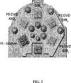
Erfindungsgemäß umfasst die Beschichtungsanlage eine induktiv gekoppelte Plasmaquelle (ICP) mit einer Reaktionskammer und mindestens einem HF-Induktor, eine Substrathalterung zur Anordnung eines Substrats, insbesondere mehrerer Substrate, in der Reaktionskammer und Kanälen zum Einleiten der Aluminiumverbindung und eines Reaktivgases in die ICP-Quelle. Das Substrat ist hierbei derart in der Reaktionskammer angeordnet, dass die zu beschichtende Oberfläche des Substrats zur ICP-Quelle weist.According to the invention, the coating installation comprises an inductively coupled plasma source (ICP) with a reaction chamber and at least one RF inductor, a substrate holder for arranging a substrate, in particular a plurality of substrates, in the reaction chamber and channels for introducing the aluminum compound and a reactive gas into the ICP source. In this case, the substrate is arranged in the reaction chamber such that the surface of the substrate to be coated faces the ICP source.
Die induktiv gekoppelte Plasmaquelle umfasst hierbei die Reaktionskammer und mindestens einen Induktor, der mit einer hochfrequenten Stromquelle verbunden ist. Auf diese Weise kann in die Reaktionskammer direkt die für die Erzeugung des Plasmas nötige Energie eingekoppelt werden. Vorzugsweise sind zudem Kanäle zum Einleiten von Reaktivgas und/oder zum Einleiten eines z. B. fluiden Präkursors (wie z. B. TMA) in die Plasmaquelle vorgesehen. Durch die Anordnung des Substrats derart, dass die zu beschichtende Oberfläche des Substrats in Richtung Plasmaquelle weist, kann die Beschichtungsrate optimiert und somit der Durchsatz der beschichteten Bauteile erhöht werden.The inductively coupled plasma source in this case comprises the reaction chamber and at least one inductor which is connected to a high-frequency power source. In this way, the energy required for the generation of the plasma can be coupled directly into the reaction chamber. Preferably also channels for introducing reactive gas and / or initiating a z. Fluid precursor (such as TMA) into the plasma source. By arranging the substrate such that the surface of the substrate to be coated points in the direction of the plasma source, the coating rate can be optimized and thus the throughput of the coated components can be increased.
In einer Ausführungsform umfasst die Beschichtungsanlage mindestens eine zweite induktiv gekoppelte Plasmaquelle (ICP) mit einer Reaktionskammer und mindestens einem HF-Induktor und Kanälen zum Einleiten einer Siliziumverbindung und eines Reaktivgases in die zweite/weiteren ICP-Quelle(n). In one embodiment, the coating equipment comprises at least one second inductively coupled plasma source (ICP) having a reaction chamber and at least one RF inductor and channels for introducing a silicon compound and a reactive gas into the second / further ICP source (s).
Vorzugsweise kann die Beschichtungsanlage derart ausgebildet sein, dass sie mehrere Prozessstationen aufweist, die mit ICP-Quellen und entsprechenden Reaktionskammern und Kanälen ausgestattet sind. In einer Ausführungsform umfasst die Beschichtungsanlage auch Transportmechanismen, so dass ein insbesondere beschichtetes Substrat von einer ersten in eine zweite Prozessstation, insbesondere in eine zweite Plasmaquelle mit Reaktionskammer zugeführt werden kann. In der zweiten Prozessstation/Quelle/Reaktionskammer kann dann eine weitere Beschichtung vorgenommen werden, insbesondere zur Herstellung einer (zu der ersten Schicht) unterschiedlichen Schicht. Zudem können noch weitere Beschichtungen in weiteren Prozessstationen/Quellen/Reaktionskammern vorgesehen werden.Preferably, the coating equipment may be configured to include a plurality of process stations equipped with ICP sources and corresponding reaction chambers and channels. In one embodiment, the coating system also includes transport mechanisms, so that a particular coated substrate can be supplied from a first to a second process station, in particular into a second plasma source with reaction chamber. In the second process station / source / reaction chamber can then be made a further coating, in particular for the production of a (to the first layer) different layer. In addition, further coatings can be provided in further process stations / sources / reaction chambers.
In einer Ausführungsform ist der Induktor der ICP-Quelle bzw. der ICP-Quellen außerhalb der zugehörigen Reaktionskammer angeordnet und von dieser durch eine dielektrische Trennwand getrennt. Vorzugsweise trennt die dielektrische Wand die Reaktionskammer von dem Bereich des Induktors mit der hochfrequenten Stromquelle derart ab, dass diese insbesondere einen Schutz für den Induktor darstellt und sich das Plasma kontrolliert und gerichtet ausbilden kann.In one embodiment, the inductor of the ICP source (s) is disposed outside the associated reaction chamber and separated therefrom by a dielectric baffle. The dielectric wall preferably separates the reaction chamber from the region of the inductor with the high-frequency current source in such a way that, in particular, it provides protection for the inductor and the plasma can form controlled and directed.
Die hier beschriebenen Verfahren und Beschichtungsanlage können z. B. zur Passivierung, insbesondere zur Rückseitenpassivierung von Solarzellen, vorzugsweise von kristallinen Solarzellen, angewendet werden.The methods and coating system described here can z. B. for passivation, in particular for the backside passivation of solar cells, preferably of crystalline solar cells, are applied.
Das erfindungsgemäße Verfahren und die entsprechende Beschichtungsanlage ermöglichen die Herstellung von qualitativ hochwertigen, defektarmen homogenen Schichten (Niederdruck). Durch die hohe Dissoziation von Sauerstoff und die hohe Umsatzrate des Aluminium-haltigen Gases, insbesondere TMA, in der Quelle wird zudem ein hoher Durchsatz an beschichteten Substraten, z. B. Solarzellen mit hoher Zelleffizienz, bei gleichzeitigem niedrigen Verbrauch an TMA ermöglicht. Auf diese Weise sinken die Materialkosten pro Wafer bzw. pro Watt deutlich.The inventive method and the corresponding coating system allow the production of high-quality, low-defect homogeneous layers (low pressure). Due to the high dissociation of oxygen and the high conversion rate of the aluminum-containing gas, in particular TMA, in the source is also a high throughput of coated substrates, eg. B. solar cells with high cell efficiency, while allowing low consumption of TMA. This significantly reduces material costs per wafer or per watt.
Ein weiterer Vorteil gegenüber bereits bekannten Verfahren bzw. Beschichtungsanlagen besteht darin, dass diese Verfahren in einer einzigen Anlage (z. B. mit mehreren Reaktionskammern, die den gleichen Druck oder unterschiedliche Drücke aufweisen, und/oder mit geeigneten Transportmechanismen zwischen den einzelnen Kammern) durchgeführt werden können: so kann z. B. der gesamte Rückseitenschichtstapel aus einer Aluminiumoxid- und einer Siliziumnitrid-Schicht in einer Plattform (eine derartige Plattform ist z. B. aus der
Einige der oben beschriebenen, insbesondere voneinander unabhängigen, Prozessparameter, insbesondere zur Aluminiumoxid-Beschichtung, können wie folgt zusammengefasst werden:
Druck: 10–4 bis 10–1 mbar, vorzugsweise von 10–3 bis 5·10–2 mbar
Substrattemperatur: Raumtemperatur bis 450°C
Radiofrequenz: 1–60 MHz, vorzugsweise 13,56 MHz
Plasmaleistung: 0,5 bis 10 kW, vorzugsweise 3,5 bis 6 kW
Ionenenergie: 1 eV bis 30 eV, vorzugsweise weniger als 20 eV
Plasmadichte: mindestens 1 × 10¹¹ Ionen/cm3, vorzugsweise von 1 × 10¹² Ionen/cm3 bis 9 × 10¹³ Ionen/cm3
Ionisationsgrad: bis zu 50%
Dissoziationsgrad: 2-atomige Moleküle (O2) bis zu 80%
Plasmaqualität: partikelfreier Plasmastrahl durch NiederdruckSome of the above-described, in particular independent, process parameters, in particular for aluminum oxide coating, can be summarized as follows:
Pressure: 10-4 to 10-1 mbar, preferably from 10-3 to 5 x 10⁻² mbar
Substrate temperature: room temperature up to 450 ° C
Radio frequency: 1-60 MHz, preferably 13.56 MHz
Plasma power: 0.5 to 10 kW, preferably 3.5 to 6 kW
Ion energy: 1 eV to 30 eV, preferably less than 20 eV
Plasma density: at least 1 × 10¹¹ ions / cm3 , preferably from 1 × 10¹² ions / cm3 to 9 × 10¹³ ions / cm3
Ionization degree: up to 50%
Degree of dissociation: 2-atom molecules (O2 ) up to 80%
Plasma quality: particle-free plasma jet due to low pressure
Die Erfindung wird nachstehend mit Bezug auf die Zeichnungen näher erläutert. Es zeigen:The invention will be explained in more detail below with reference to the drawings. Show it:
Nach der direkten induktiven Einkopplung der Energie, entsteht ein Plasma
Alternativ ist es auch möglich, dass das Substrat in einer Halterung verbleibt und die einzelnen Stationen/Quellen/Kammern an eine Seite des Substrat angebracht werden können (z. B. durch Drehung der Ebene der Kammern parallel zur Substratebene), so dass das Substrat beschichtet werden kann.Alternatively, it is also possible that the substrate remains in a holder and the individual stations / sources / chambers can be attached to one side of the substrate (eg by rotation of the plane of the chambers parallel to the substrate plane) so that the substrate coats can be.
Dabei ist es jeweils möglich, ein Substrat in einer Anlage mit verschiedenen Materialien zu beschichten. Zum Beispiel kann auf das Substrat zunächst eine Aluminiumoxid-Schicht unter Nutzung von TMA als Präkursor und Sauerstoff als Reaktivgas abgeschieden werden, und danach unter Nutzung von SiH4 als Präkursor und NH3 als Reaktivgas eine Siliziumnitrid-Schicht auf die Aluminiumoxid-Schicht aufgebracht werden.It is in each case possible to coat a substrate in a plant with different materials. For example, an aluminum oxide layer may first be deposited on the substrate using TMA as a precursor and oxygen as a reactive gas, and then a silicon nitride layer may be applied to the aluminum oxide layer using SiH4 as the precursor and NH3 as the reactive gas.
Das erfindungsgemäße Verfahren und die entsprechende Beschichtungsanlage ermöglichen somit die Herstellung von qualitativ hochwertigen Schichten bei niedrigem Prozessdruck und geringen Materialkosten. Ein weiterer Vorteil gegenüber bereits bekannten Verfahren bzw. Beschichtungsanlagen besteht darin, dass diese Verfahren in einer einzigen Anlage durchgeführt werden können, so dass sich die Zykluszeit verkürzt und sich damit der Durchsatz erhöht.The inventive method and the corresponding coating system thus enable the production of high-quality layers at low process pressure and low material costs. Another advantage over already known methods or coating systems is that these methods can be performed in a single system, so that the cycle time is shortened and thus increases the throughput.
ZITATE ENTHALTEN IN DER BESCHREIBUNG QUOTES INCLUDE IN THE DESCRIPTION
Diese Liste der vom Anmelder aufgeführten Dokumente wurde automatisiert erzeugt und ist ausschließlich zur besseren Information des Lesers aufgenommen. Die Liste ist nicht Bestandteil der deutschen Patent- bzw. Gebrauchsmusteranmeldung. Das DPMA übernimmt keinerlei Haftung für etwaige Fehler oder Auslassungen.This list of the documents listed by the applicant has been generated automatically and is included solely for the better information of the reader. The list is not part of the German patent or utility model application. The DPMA assumes no liability for any errors or omissions.
Zitierte PatentliteraturCited patent literature
- DE 102007054384 A1[0004]DE 102007054384 A1[0004]
- DE 102009018700[0031]DE 102009018700[0031]
Claims (14)
Translated fromGermanPriority Applications (7)
| Application Number | Priority Date | Filing Date | Title |
|---|---|---|---|
| DE102012201953ADE102012201953A1 (en) | 2012-02-09 | 2012-02-09 | Method and device for passivation of solar cells with an aluminum oxide layer |
| MYPI2014702183AMY169705A (en) | 2012-02-09 | 2013-02-06 | Method and device for passivating solar cells with an aluminium oxide layer |
| EP13707119.7AEP2812461B1 (en) | 2012-02-09 | 2013-02-06 | Method for passivating solar cells with an aluminium oxide layer |
| PCT/EP2013/052298WO2013117576A1 (en) | 2012-02-09 | 2013-02-06 | Method and device for passivating solar cells with an aluminium oxide layer |
| KR1020147022043AKR20140128322A (en) | 2012-02-09 | 2013-02-06 | Method and device for passivating solar cells with an aluminium oxide layer |
| CN201380008784.6ACN104105814B (en) | 2012-02-09 | 2013-02-06 | Method and apparatus for passivating solar cells using an aluminum oxide layer |
| US14/377,317US20150004331A1 (en) | 2012-02-09 | 2013-02-06 | Method and device for passivating solar cells with an aluminium oxide layer |
Applications Claiming Priority (1)
| Application Number | Priority Date | Filing Date | Title |
|---|---|---|---|
| DE102012201953ADE102012201953A1 (en) | 2012-02-09 | 2012-02-09 | Method and device for passivation of solar cells with an aluminum oxide layer |
Publications (1)
| Publication Number | Publication Date |
|---|---|
| DE102012201953A1true DE102012201953A1 (en) | 2013-08-14 |
Family
ID=47780024
Family Applications (1)
| Application Number | Title | Priority Date | Filing Date |
|---|---|---|---|
| DE102012201953ACeasedDE102012201953A1 (en) | 2012-02-09 | 2012-02-09 | Method and device for passivation of solar cells with an aluminum oxide layer |
Country Status (7)
| Country | Link |
|---|---|
| US (1) | US20150004331A1 (en) |
| EP (1) | EP2812461B1 (en) |
| KR (1) | KR20140128322A (en) |
| CN (1) | CN104105814B (en) |
| DE (1) | DE102012201953A1 (en) |
| MY (1) | MY169705A (en) |
| WO (1) | WO2013117576A1 (en) |
Cited By (1)
| Publication number | Priority date | Publication date | Assignee | Title |
|---|---|---|---|---|
| DE102018004086A1 (en)* | 2018-05-18 | 2019-11-21 | Singulus Technologies Ag | Continuous flow system and method for coating substrates |
Families Citing this family (4)
| Publication number | Priority date | Publication date | Assignee | Title |
|---|---|---|---|---|
| KR101881534B1 (en)* | 2016-02-04 | 2018-07-24 | 주식회사 테스 | Method for formation of carbon layer including metal-oxide using plasmas |
| CN107623052B (en)* | 2017-09-01 | 2023-12-05 | 常州比太科技有限公司 | Al for passivation of solar cell 2 O 3 Coating system and method |
| CN110699674B (en)* | 2019-10-10 | 2021-12-24 | 湖南红太阳光电科技有限公司 | Method for depositing aluminum oxide by low-frequency PECVD |
| CN113097341B (en)* | 2021-03-31 | 2023-10-31 | 通威太阳能(安徽)有限公司 | A PERC battery, its AlOx coating process, multi-layer AlOx back passivation structure and method |
Citations (7)
| Publication number | Priority date | Publication date | Assignee | Title |
|---|---|---|---|---|
| DE2538300A1 (en)* | 1975-08-28 | 1977-03-03 | Dornier System Gmbh | Device absorbing sun light in semiconductive coating - formed by deposition from vapour phase |
| DE3206421A1 (en)* | 1982-02-23 | 1983-09-01 | Siemens AG, 1000 Berlin und 8000 München | METHOD FOR PRODUCING LAYERS FROM HIGH-MELTING METALS OR METAL COMPOUNDS THROUGH VAPOR PHASE DEPOSITION |
| GB2326886A (en)* | 1997-06-30 | 1999-01-06 | Lam Res Corp | Process for depositing nitrided fluorine doped SiOx films |
| DE102007054384A1 (en) | 2007-11-14 | 2009-05-20 | Institut Für Solarenergieforschung Gmbh | Method for producing a solar cell with a surface-passivating dielectric double layer and corresponding solar cell |
| DE102009018700A1 (en) | 2008-09-01 | 2010-03-04 | Singulus Technologies Ag | coating plant |
| DE102010000002A1 (en)* | 2010-01-04 | 2011-07-07 | Roth & Rau AG, 09337 | Method for depositing multilayer films and / or gradient films |
| US20110293853A1 (en)* | 2009-02-13 | 2011-12-01 | Mitsui Engineering & Shipbuilding Co., Ltd | Thin film forming apparatus and thin film forming method |
Family Cites Families (13)
| Publication number | Priority date | Publication date | Assignee | Title |
|---|---|---|---|---|
| US20020004309A1 (en)* | 1990-07-31 | 2002-01-10 | Kenneth S. Collins | Processes used in an inductively coupled plasma reactor |
| US6070551A (en)* | 1996-05-13 | 2000-06-06 | Applied Materials, Inc. | Deposition chamber and method for depositing low dielectric constant films |
| US5846883A (en)* | 1996-07-10 | 1998-12-08 | Cvc, Inc. | Method for multi-zone high-density inductively-coupled plasma generation |
| US6013584A (en)* | 1997-02-19 | 2000-01-11 | Applied Materials, Inc. | Methods and apparatus for forming HDP-CVD PSG film used for advanced pre-metal dielectric layer applications |
| WO2000063956A1 (en)* | 1999-04-20 | 2000-10-26 | Sony Corporation | Method and apparatus for thin-film deposition, and method of manufacturing thin-film semiconductor device |
| US7087537B2 (en)* | 2004-03-15 | 2006-08-08 | Sharp Laboratories Of America, Inc. | Method for fabricating oxide thin films |
| US7544625B2 (en)* | 2003-01-31 | 2009-06-09 | Sharp Laboratories Of America, Inc. | Silicon oxide thin-films with embedded nanocrystalline silicon |
| US6982448B2 (en)* | 2004-03-18 | 2006-01-03 | Texas Instruments Incorporated | Ferroelectric capacitor hydrogen barriers and methods for fabricating the same |
| CA2597623C (en)* | 2005-02-28 | 2015-07-14 | Epispeed S.A. | System and process for high-density,low-energy plasma enhanced vapor phase epitaxy |
| US7727828B2 (en)* | 2005-10-20 | 2010-06-01 | Applied Materials, Inc. | Method for fabricating a gate dielectric of a field effect transistor |
| KR20070099913A (en)* | 2006-04-06 | 2007-10-10 | 주성엔지니어링(주) | Oxide film formation method and oxide film deposition apparatus |
| US8025932B2 (en)* | 2007-02-21 | 2011-09-27 | Colorado School Of Mines | Self-limiting thin film synthesis achieved by pulsed plasma-enhanced chemical vapor deposition |
| CN102064237A (en)* | 2010-11-29 | 2011-05-18 | 奥特斯维能源(太仓)有限公司 | Double-layer passivating method for crystalline silicon solar battery |
- 2012
- 2012-02-09DEDE102012201953Apatent/DE102012201953A1/ennot_activeCeased
- 2013
- 2013-02-06KRKR1020147022043Apatent/KR20140128322A/ennot_activeCeased
- 2013-02-06WOPCT/EP2013/052298patent/WO2013117576A1/enactiveApplication Filing
- 2013-02-06EPEP13707119.7Apatent/EP2812461B1/enactiveActive
- 2013-02-06MYMYPI2014702183Apatent/MY169705A/enunknown
- 2013-02-06USUS14/377,317patent/US20150004331A1/ennot_activeAbandoned
- 2013-02-06CNCN201380008784.6Apatent/CN104105814B/enactiveActive
Patent Citations (7)
| Publication number | Priority date | Publication date | Assignee | Title |
|---|---|---|---|---|
| DE2538300A1 (en)* | 1975-08-28 | 1977-03-03 | Dornier System Gmbh | Device absorbing sun light in semiconductive coating - formed by deposition from vapour phase |
| DE3206421A1 (en)* | 1982-02-23 | 1983-09-01 | Siemens AG, 1000 Berlin und 8000 München | METHOD FOR PRODUCING LAYERS FROM HIGH-MELTING METALS OR METAL COMPOUNDS THROUGH VAPOR PHASE DEPOSITION |
| GB2326886A (en)* | 1997-06-30 | 1999-01-06 | Lam Res Corp | Process for depositing nitrided fluorine doped SiOx films |
| DE102007054384A1 (en) | 2007-11-14 | 2009-05-20 | Institut Für Solarenergieforschung Gmbh | Method for producing a solar cell with a surface-passivating dielectric double layer and corresponding solar cell |
| DE102009018700A1 (en) | 2008-09-01 | 2010-03-04 | Singulus Technologies Ag | coating plant |
| US20110293853A1 (en)* | 2009-02-13 | 2011-12-01 | Mitsui Engineering & Shipbuilding Co., Ltd | Thin film forming apparatus and thin film forming method |
| DE102010000002A1 (en)* | 2010-01-04 | 2011-07-07 | Roth & Rau AG, 09337 | Method for depositing multilayer films and / or gradient films |
Cited By (2)
| Publication number | Priority date | Publication date | Assignee | Title |
|---|---|---|---|---|
| DE102018004086A1 (en)* | 2018-05-18 | 2019-11-21 | Singulus Technologies Ag | Continuous flow system and method for coating substrates |
| WO2019219292A2 (en) | 2018-05-18 | 2019-11-21 | Singulus Technologies Ag | Continuous flow system and method for coating substrates |
Also Published As
| Publication number | Publication date |
|---|---|
| WO2013117576A1 (en) | 2013-08-15 |
| KR20140128322A (en) | 2014-11-05 |
| CN104105814A (en) | 2014-10-15 |
| CN104105814B (en) | 2017-10-24 |
| US20150004331A1 (en) | 2015-01-01 |
| EP2812461A1 (en) | 2014-12-17 |
| EP2812461B1 (en) | 2016-11-09 |
| MY169705A (en) | 2019-05-13 |
Similar Documents
| Publication | Publication Date | Title |
|---|---|---|
| EP2521803B1 (en) | Method for depositing multi-layered layers and/or gradient layers | |
| EP2812461B1 (en) | Method for passivating solar cells with an aluminium oxide layer | |
| DE102008019023A1 (en) | Vacuum continuous flow system for the processing of substrates | |
| US20230298885A1 (en) | Methods for depositing gap-filling fluids and related systems and devices | |
| EP3794159A2 (en) | Continuous flow system and method for coating substrates | |
| DE102010000001A1 (en) | Inline coating machine | |
| EP2459767A1 (en) | Cleaning of a process chamber | |
| WO2018193055A1 (en) | Method and device for forming a layer on a semiconductor substrate, and semiconductor substrate | |
| DE102008028542A1 (en) | Method and apparatus for depositing a layer on a substrate by means of a plasma-enhanced chemical reaction | |
| WO2020069700A1 (en) | Solar-cell coating system | |
| DE102020124030B4 (en) | Apparatus, system and method for plasma enhanced chemical vapor deposition | |
| DE102013112785B3 (en) | Method for producing a composite body with at least one functional layer or for further production of electronic or opto-electronic components | |
| DE102017108290B4 (en) | Plasma device | |
| DE102009018700B4 (en) | Coating line and method for coating | |
| EP1038306B1 (en) | Method and device for improving surfaces | |
| EP0257620B1 (en) | Method and device for forming a layer by a chemical plasma process | |
| EP1854907B1 (en) | Device for plasma-based chemical treatment of surfaces of substrates in a vacuum | |
| DE102018132700A1 (en) | Device and method for coating and in particular plasma coating of containers | |
| DE102007031416B4 (en) | Substrate made of a polymeric material and having a water- and oxygen-impermeable barrier coating and associated manufacturing method | |
| DE102009026249A1 (en) | Plasma assisted deposition process, semiconductor device and deposition device | |
| DE102012219667A1 (en) | Method for applying aluminum oxide layer on semiconductor substrate for photovoltaic solar cell, involves creating plasma zone between supply point of aluminum-containing gas and suction location of gases in process chamber | |
| DE4425626A1 (en) | Method and appts. for plasma coating components with metal and polymer layers | |
| DE10141142B4 (en) | Device for reactive plasma treatment of substrates and method for use | |
| DE102011113751A1 (en) | METHOD FOR THE STEADY AND / OR SEQUENTIAL SEPARATION OF A DIELECTRIC LAYER FROM THE GAS PHASE ON A SUBSTRATE | |
| DE102007016026A1 (en) | Vacuum coating apparatus, especially CVD apparatus, has HF or microwave source, especially magnetron, mounted between coating chamber and vacuum pump to treat residual gases |
Legal Events
| Date | Code | Title | Description |
|---|---|---|---|
| R012 | Request for examination validly filed | ||
| R002 | Refusal decision in examination/registration proceedings | ||
| R003 | Refusal decision now final |