DE102012108097A1 - Touch controls, methods thereof, and touch control devices - Google Patents
Touch controls, methods thereof, and touch control devicesDownload PDFInfo
- Publication number
- DE102012108097A1 DE102012108097A1DE102012108097ADE102012108097ADE102012108097A1DE 102012108097 A1DE102012108097 A1DE 102012108097A1DE 102012108097 ADE102012108097 ADE 102012108097ADE 102012108097 ADE102012108097 ADE 102012108097ADE 102012108097 A1DE102012108097 A1DE 102012108097A1
- Authority
- DE
- Germany
- Prior art keywords
- current
- control
- touch
- channels
- output voltage
- Prior art date
- Legal status (The legal status is an assumption and is not a legal conclusion. Google has not performed a legal analysis and makes no representation as to the accuracy of the status listed.)
- Pending
Links
Images


Classifications
- G—PHYSICS
- G06—COMPUTING OR CALCULATING; COUNTING
- G06F—ELECTRIC DIGITAL DATA PROCESSING
- G06F3/00—Input arrangements for transferring data to be processed into a form capable of being handled by the computer; Output arrangements for transferring data from processing unit to output unit, e.g. interface arrangements
- G06F3/01—Input arrangements or combined input and output arrangements for interaction between user and computer
- G06F3/03—Arrangements for converting the position or the displacement of a member into a coded form
- G06F3/041—Digitisers, e.g. for touch screens or touch pads, characterised by the transducing means
- G06F3/044—Digitisers, e.g. for touch screens or touch pads, characterised by the transducing means by capacitive means
- G06F3/0443—Digitisers, e.g. for touch screens or touch pads, characterised by the transducing means by capacitive means using a single layer of sensing electrodes
- G—PHYSICS
- G06—COMPUTING OR CALCULATING; COUNTING
- G06F—ELECTRIC DIGITAL DATA PROCESSING
- G06F3/00—Input arrangements for transferring data to be processed into a form capable of being handled by the computer; Output arrangements for transferring data from processing unit to output unit, e.g. interface arrangements
- G06F3/01—Input arrangements or combined input and output arrangements for interaction between user and computer
- G06F3/03—Arrangements for converting the position or the displacement of a member into a coded form
- G06F3/041—Digitisers, e.g. for touch screens or touch pads, characterised by the transducing means
- G06F3/0416—Control or interface arrangements specially adapted for digitisers
- G06F3/0418—Control or interface arrangements specially adapted for digitisers for error correction or compensation, e.g. based on parallax, calibration or alignment
- G06F3/04184—Synchronisation with the driving of the display or the backlighting unit to avoid interferences generated internally
- H—ELECTRICITY
- H03—ELECTRONIC CIRCUITRY
- H03K—PULSE TECHNIQUE
- H03K17/00—Electronic switching or gating, i.e. not by contact-making and –breaking
- H03K17/94—Electronic switching or gating, i.e. not by contact-making and –breaking characterised by the way in which the control signals are generated
- H03K17/96—Touch switches
- H03K17/962—Capacitive touch switches
- H03K17/9622—Capacitive touch switches using a plurality of detectors, e.g. keyboard
Landscapes
- Engineering & Computer Science (AREA)
- General Engineering & Computer Science (AREA)
- Theoretical Computer Science (AREA)
- Human Computer Interaction (AREA)
- Physics & Mathematics (AREA)
- General Physics & Mathematics (AREA)
- Control Of Indicators Other Than Cathode Ray Tubes (AREA)
- Position Input By Displaying (AREA)
- Liquid Crystal Display Device Control (AREA)
Abstract
Translated fromGermanDescription
Translated fromGermanQUERVERWEIS AUF VERWANDTE ANMELDUNGENCROSS-REFERENCE TO RELATED APPLICATIONS
Diese Anmeldung beansprucht die Priorität der vorläufigen US-Patentanmeldung US 61/532,697, eingereicht am 9. September 2011, und unter 35 U.S.C. § 119 (a) der
HINTERGRUNDBACKGROUND
Beispielhafte Ausführungsformen der erfinderischen Idee beziehen sich auf eine Berührungssteuerung und insbesondere auf eine Berührungssteuerung zum Entfernen eines Anzeigerauschens in einer gemeinsamen Anzeigeelektrode, ein Betriebsverfahren davon und Vorrichtungen mit der Berührungssteuerung.Exemplary embodiments of the inventive concept relate to touch control, and more particularly to touch control for removing display noise in a common display electrode, an operating method thereof, and touch-control devices.
Die Nachfrage nach einer berührbaren elektronischen Vorrichtung nimmt zu. Die berührbare elektronische Vorrichtung weist ein Berührungs-Anzeigefeld zum Erfassen einer Berührung auf. Das Berührungs-Anzeigefeld weist eine Sensorelektrode zum Messen von Kapazitätsänderungen auf.The demand for a touchable electronic device is increasing. The touchable electronic device has a touch panel for detecting a touch. The touch panel has a sensor electrode for measuring capacitance changes.
Eine kapazitive Berührungsabtastung erfasst eine Berührung durch die Verwendung einer Kapazitätsänderung. Wenn ein Finger oder leitfähiger Eingabestift eine Sensorelektrode berührt, ändert sich die Kapazität. Eine Kapazitätsänderung kann durch die Sensorelektrode gemessen werden und die Kapazitätsänderung kann in eine Position von X und Y umgewandelt werden.A capacitive touch scan detects a touch through the use of a capacitance change. When a finger or conductive stylus touches a sensor electrode, the capacitance changes. A capacitance change can be measured by the sensor electrode, and the capacitance change can be converted to a position of X and Y.
Das Berührungs-Anzeigefeld weist eine gemeinsame Anzeigeelektrode auf, um ein Bild darzustellen. Da eine Stärke des Berührungs-Anzeigefelds dünner wird, kann ein in der gemeinsamen Anzeigeelektrode erzeugtes Anzeigerauschen die Berührungserfassung beeinträchtigen. Das Anzeigerauschen kann durch das Material, einer Struktur der gemeinsamen Anzeigeelektrode oder ein dargestelltes Bild erzeugt werden.The touch panel has a common display electrode to display an image. As a thickness of the touch panel becomes thinner, a display noise generated in the common display electrode may affect the touch detection. The display noise may be generated by the material, a common display electrode structure, or a displayed image.
KURZFASSUNGSHORT VERSION
Eine beispielhafte Ausführungsform bezieht sich auf ein Betriebsverfahren einer Berührungssteuerung, das ein Empfangen jedes einer Mehrzahl von Strömen durch jeden einer Mehrzahl von Kanälen, Abtasten eines ersten Stroms unter der Mehrzahl von Strömen und Entnehmen des abgetasteten ersten Stroms als einen ersten Steuerstrom und Umwandeln einer Ladung, die einer Differenz zwischen dem ersten Steuerstrom und einem zweiten Strom unter der Mehrzahl von Strömen entspricht, in eine Ausgangsspannung aufweist.An exemplary embodiment relates to an operation method of touch control, receiving each of a plurality of currents through each of a plurality of channels, sampling a first current among the plurality of currents, and extracting the sampled first current as a first control current and converting a charge; which corresponds to a difference between the first control current and a second current among the plurality of currents, in an output voltage.
Gemäß einer beispielhaften Ausführungsform kann ein Betriebsverfahren der Berührungssteuerung ferner ein Auswählen des jeweiligen Kanals des ersten Stroms und des jeweiligen Kanals des zweiten Stroms als Antwort auf ein Auswahlsignal aufweisen.According to an exemplary embodiment, an operation method of the touch control may further comprise selecting the respective channel of the first stream and the respective channel of the second stream in response to a selection signal.
Das Umwandeln in eine Ausgangsspannung weist das Umwandeln einer Stromdifferenz zwischen dem zweiten Strom und dem ersten Steuerstrom in eine Ausgangsspannung auf.Converting to an output voltage comprises converting a current difference between the second current and the first control current into an output voltage.
Gemäß einer beispielhaften Ausführungsform kann das Betriebsverfahren der Berührungssteuerung ein Kompensieren einer Nichtübereinstimmung zwischen einer Mehrzahl von parasitären Elementen zwischen einer gemeinsamen Anzeigeelektrode und einer Sensorelektrode als Antwort auf die Ausgangsspannung aufweisen.According to an exemplary embodiment, the touch control operation method may include compensating for a mismatch between a plurality of parasitic elements between a common display electrode and a sensor electrode in response to the output voltage.
Das Kompensieren der Nichtübereinstimmung zwischen der Mehrzahl von parasitären Elementen weist ein Vergleichen der Ausgangsspannung mit einer Vergleichsspannung und ein Ausgeben einer Mehrzahl von Auswahl-Bits gemäß einem Vergleichsergebnis und ein Kompensieren der Nichtübereinstimmung durch Auswählen von mindestens einem von einer Mehrzahl von Kondensatoren gemäß der Mehrzahl von Auswahl-Bits und ein Kompensieren der Nichtübereinstimmung basierend auf dem mindestens einen ausgewählten Kondensator auf.Compensating the mismatch between the plurality of parasitic elements comprises comparing the output voltage with a comparison voltage and outputting a plurality of selection bits according to a comparison result and compensating the mismatch by selecting at least one of a plurality of capacitors according to the plurality of choices Bits and compensating the mismatch based on the at least one selected capacitor.
Gemäß einer beispielhaften Ausführungsform das Umwandeln und das Entnehmen des abgetasteten zweiten Stroms als einen zweiten Steuerstrom, und Umwandeln der Stromdifferenz zwischen dem zweiten Steuerstrom und dem ersten Steuerstrom in die Ausgangsspannung.According to an example embodiment, converting and extracting the sampled second current as a second control current, and converting the current difference between the second control current and the first control current into the output voltage.
Eine beispielhafte Ausführungsform der erfinderischen Idee bezieht sich auf eine Berührungssteuerung mit einer Mehrzahl von Kontakten, wobei jeder mit einem von einer Mehrzahl von Kanälen gekoppelt ist, eine Auswahlvorrichtung zum Auswählen von zwei Kanälen unter der Mehrzahl von Kanälen als Antwort auf ein Auswahlsignal und einen Differenz-Abtastblock, der derart konfiguriert ist, dass er eine Ladung gemäß einer Differenz zwischen einem ersten Strom und einem zweiten Strom, die in jedem der beiden Kanäle fließen, in eine Ausgangsspannung umwandelt.An exemplary embodiment of the inventive concept relates to a touch control with a plurality of contacts, each coupled to one of a plurality of channels, a selector for selecting two channels among the plurality of channels in response to a selection signal and a difference signal. A sample block configured to convert a charge into an output voltage according to a difference between a first current and a second current flowing in each of the two channels.
Der Differenz-Abtastblock weist einen Current Conveyor auf, der derart konfiguriert ist, dass er den ersten Strom abtastet und den abgetasteten ersten Strom als einen Steuerstrom entnimmt und einen Ladungsverstärker, der derart konfiguriert ist, dass er eine Stromdifferenz zwischen dem zweiten Strom und dem Steuerstrom in die Ausgangsspannung umwandelt.The differential sample block has a current conveyor configured to sample the first stream and the sampled one takes first current as a control current and a charge amplifier configured to convert a current difference between the second current and the control current into the output voltage.
Der Current Conveyor weist eine erste Eingangsklemme auf, die derart konfiguriert ist, dass sie den ersten Strom empfängt, eine zweite Eingangsklemme auf, die derart konfiguriert ist, dass sie eine Wechselspannung empfängt, und einen Trennverstärker mit Verstärkungsfaktor Eins mit einer ersten Ausgangsklemme auf, die mit der ersten Eingangsklemme gekoppelt ist und einen Strom-Kopierer-Schaltkreis mit einer zweiten Ausgangsklemme, den Strom-Kopierer-Schaltkreis zum Entnehmen des Steuerstroms gemäß einer Mehrzahl von Steuerspannungen auf, die von dem Trennverstärker mit Verstärkungsfaktor Eins ausgegeben werden.The current conveyor has a first input terminal configured to receive the first current, a second input terminal configured to receive an AC voltage, and a unity gain isolation amplifier having a first output terminal coupled to the first input terminal and a current copier circuit having a second output terminal, the current copier circuit for extracting the control current according to a plurality of control voltages output from the unity gain isolation amplifier.
Der Strom-Kopierer-Schaltkreis weist einen stromliefernden Schaltkreis und einen stromableitenden Schaltkreis auf, die zwischen einem Spannungs-Knoten und einem Masse-Knoten des Trennverstärkers mit Verstärkungsfaktor Eins in Reihe gekoppelt sind.The current copier circuit includes a current sourcing circuit and a current sinking circuit coupled in series between a voltage node and a ground node of the unity gain isolation amplifier.
Jeder des stromliefernden Schaltkreises und des stromableitenden Schaltkreises wird durch eine Mehrzahl von Steuerspannungen gesteuert. Der Steuerstrom ist eine Stromdifferenz zwischen einem in dem stromliefernden Schaltkreis fließenden Strom und einem in dem stromableitenden Schaltkreis fließenden Strom. Wenn eine Mehrzahl von mit einer Mehrzahl von Kanälen gekoppelten Sensoren nicht berührt wird, ist die Ausgangsspannung eine Referenzspannung.Each of the current-supplying circuit and the current-draining circuit is controlled by a plurality of control voltages. The control current is a current difference between a current flowing in the power-supplying circuit and a current flowing in the current-draining circuit. When a plurality of sensors coupled to a plurality of channels are not touched, the output voltage is a reference voltage.
Gemäß einer beispielhaften Ausführungsform kann die Berührungssteuerung ferner einen Nichtübereinstimmungs-Kompensationsblock aufweisen, der mit der gemeinsamen Anzeigeelektrode gekoppelt ist, wobei der Nichtübereinstimmungs-Kompensationsblock derart konfiguriert ist, dass er eine Nichtübereinstimmung zwischen einer Mehrzahl von parasitären Elementen zwischen einer gemeinsamen Anzeigeelektrode und einer Sensorelektrode als Antwort auf die Ausgangsspannung kompensiert. Der Nichtübereinstimmungs-Kompensationsblock weist eine Kondensator-Matrix mit einer Mehrzahl von Kondensatoren und einen Auswahl-Bit-Generator auf, der derart konfiguriert ist, dass er die Ausgangsspannung mit einer Vergleichsspannung vergleicht, um mindestens einen der Mehrzahl von Kondensatoren auszuwählen und eine Mehrzahl von Auswahl-Bits gemäß einem Vergleichsergebnis zu erzeugen.According to an exemplary embodiment, the touch controller may further include a mismatch compensation block coupled to the common display electrode, the mismatch compensation block being configured to respond in a mismatch between a plurality of parasitic elements between a common display electrode and a sensor electrode compensated for the output voltage. The mismatch compensation block comprises a capacitor array having a plurality of capacitors and a select bit generator configured to compare the output voltage with a comparison voltage to select at least one of the plurality of capacitors and a plurality of selections To generate bits according to a comparison result.
Der Auswahl-Bit-Generator weist einen Komparator auf, der derart konfiguriert ist, dass er die Vergleichsspannung mit der Ausgangsspannung vergleicht und ein Vergleichssignal ausgibt und eine SAR-Steuerlogik aufweist, die derart konfiguriert ist, dass sie die Mehrzahl von Auswahl-Bits als Antwort auf das Vergleichssignal erzeugt.The select bit generator has a comparator configured to compare the comparison voltage with the output voltage and output a comparison signal and having SAR control logic configured to respond the plurality of select bits in response generated on the comparison signal.
Die SAR-Steuerlogik erzeugt ein Kompensations-Taktsignal und liefert das Kompensations-Taktsignal an einen Source-Treiber.The SAR control logic generates a compensation clock signal and provides the compensation clock signal to a source driver.
Noch eine weitere beispielhafte Ausführungsform der erfinderischen Idee bezieht sich auf eine Berührungssteuerung mit einer Mehrzahl von Kontakten, wobei jeder mit einer Mehrzahl von Kanälen gekoppelt ist, einen ersten Current Conveyor, der derart konfiguriert ist, dass er einen ersten in einem der Mehrzahl von Kanälen fließenden Strom abtastet und den abgetasteten ersten Strom als einen ersten Steuerstrom entnimmt, einen zweiten Current Conveyor, der derart konfiguriert ist, dass er einen zweiten in einem anderen Kanal unter der Mehrzahl von Kanälen fließenden Strom abtastet und den abgetasteten zweiten Strom als einen zweiten Steuerstrom entnimmt und einen Ladungsverstärker, der derart konfiguriert ist, dass er eine Stromdifferenz zwischen dem ersten Steuerstrom und dem zweiten Steuerstrom in eine Ausgangspannung umwandelt.Yet another exemplary embodiment of the inventive concept relates to a touch controller having a plurality of contacts, each coupled to a plurality of channels, a first current conveyor configured to flow a first one flowing in one of the plurality of channels Scans current and extracts the sampled first current as a first control current; a second current conveyor configured to sample a second current flowing in a different channel among the plurality of channels and extract the sampled second current as a second control current; a charge amplifier configured to convert a current difference between the first control current and the second control current into an output voltage.
Gemäß einer beispielhaften Ausführungsform kann die Berührungssteuerung ferner eine Mehrzahl von Treiber-Kontakten aufweisen, die mit der Mehrzahl von Treiber-Kanälen gekoppelt ist, und einen integrierten Schaltkreis aufweisen, der derart konfiguriert ist, das er ein Signal-Impulskennzeichen an jeden der Mehrzahl von Treiber-Kanälen liefert.According to an exemplary embodiment, the touch controller may further include a plurality of driver contacts coupled to the plurality of driver channels and an integrated circuit configured to apply a signal pulse tag to each of the plurality of drivers Channels.
Der erste Current Conveyor weist eine invertierende Eingangsklemme auf, die derart konfiguriert ist, dass sie den ersten Strom empfängt, eine nicht-invertierende Eingangsklemme, die derart konfiguriert ist, dass sie eine Referenzspannung empfängt, einen Trennverstärker mit Verstärkungsfaktor Eins mit einer Ausgangsklemme, die mit der invertierenden Klemme gekoppelt ist, und einen Strom-Kopierer-Schaltkreis, der derart konfiguriert ist, dass er den ersten Steuerstrom gemäß einer Mehrzahl von Steuerspannungen entnimmt, die von dem Trennverstärker mit Verstärkungsfaktor Eins ausgegeben werden, auf.The first current conveyor has an inverting input terminal configured to receive the first current, a non-inverting input terminal configured to receive a reference voltage, a unity gain isolation amplifier having an output terminal connected to is coupled to the inverting terminal, and a current copier circuit configured to extract the first control current according to a plurality of control voltages output from the unity gain isolation amplifier.
Der Strom-Kopierer-Schaltkreis weist einen stromliefernden Schaltkreis und einen stromableitenden Schaltkreis auf, die zwischen einem Spannungs-Knoten und einem Masse-Knoten des Trennverstärkers mit Verstärkungsfaktor Eins in Reihe gekoppelt sind. Jeder des stromliefernden Schaltkreises und des stromableitenden Schaltkreises ist derart konfiguriert, dass sie basierend auf der Mehrzahl von Steuerspannungen arbeiten.The current copier circuit includes a current sourcing circuit and a current sinking circuit coupled in series between a voltage node and a ground node of the unity gain isolation amplifier. Each of the current-supplying circuit and the current-draining circuit is configured to operate based on the plurality of control voltages.
Der zweite Current Conveyor weist einen Trennverstärker mit Verstärkungsfaktor Eins mit einer invertierenden Eingangsklemme auf, die derart konfiguriert ist, dass sie den zweiten Strom empfängt, eine nicht-invertierende Eingangsklemme, die derart konfiguriert ist, dass sie eine Referenzspannung empfängt und eine Ausgangsklemme, die mit der invertierenden Klemme gekoppelt ist und einen Strom-Kopierer-Schaltkreis, der derart konfiguriert ist, dass er den zweiten Steuerstrom gemäß einer Mehrzahl von Steuerspannungen entnimmt, die von dem Trennverstärker mit Verstärkungsfaktor Eins ausgegeben werden, auf. The second current conveyor has a unity gain isolation amplifier with an inverting input terminal configured to receive the second current, a non-inverting input terminal configured to receive a reference voltage, and an output terminal that receives is coupled to the inverting terminal and a current copier circuit configured to extract the second control current in accordance with a plurality of control voltages output from the unity gain isolation amplifier.
Der Strom-Kopierer-Schaltkreis weist eine Mehrzahl von Stromspiegeln auf, wobei jeder zwischen einem Spannungs-Knoten und einem Masse-Knoten des Trennverstärkers mit Verstärkungsfaktor Eins gekoppelt ist. Jeder der Mehrzahl von Stromspiegeln ist derart konfiguriert, dass er basierend auf der Mehrzahl von Steuerspannungen arbeitet.The current copier circuit has a plurality of current mirrors, each coupled between a voltage node and a ground node of the unity gain isolation amplifier. Each of the plurality of current mirrors is configured to operate based on the plurality of control voltages.
Eine beispielhafte Ausführungsform der erfinderischen Idee bezieht sich auf ein Berührungs-Anzeigesystem mit einem Berührungs-Anzeigefeld und einer Berührungssteuerung, die mit dem Berührungs-Anzeigefeld durch eine Mehrzahl von Kanälen gekoppelt ist.An exemplary embodiment of the inventive concept relates to a touch display system having a touch panel and a touch controller coupled to the touch panel by a plurality of channels.
Die Berührungssteuerung weist einen Current Conveyor auf, der einen ersten Strom unter einer Mehrzahl von durch jeden der Mehrzahl von Kanälen fließenden Strömen abtastet und den abgetasteten ersten Strom als einen Steuerstrom entnimmt und einen Ladungsverstärker, der eine Differenz zwischen dem Steuerstrom und einem zweiten Strom unter der Mehrzahl von Strömen in eine Ausgangsspannung umwandelt. Das Berührungs-Anzeigesystem ist eine tragbare Vorrichtung.The touch controller includes a current conveyor that samples a first current among a plurality of currents flowing through each of the plurality of channels and extracts the sampled first current as a control current and a charge amplifier that extracts a difference between the control current and a second current among the Converts a plurality of currents into an output voltage. The touch display system is a portable device.
Eine weitere beispielhafte Ausführungsform offenbart ein Berührungs-Anzeigesystem mit einem Anzeigefeld, das derart konfiguriert ist, dass es jeweils eine Mehrzahl von Strömen über eine Mehrzahl von Kanälen erzeugt, einen integrierten Schaltkreis, der mit der Mehrzahl von Kanälen gekoppelt ist, wobei der integrierte Schaltkreis einen Differenz-Sensor aufweist, der derart konfiguriert ist, dass er einen mit einem ersten Kanal in Verbindung stehenden ersten Strom und einen mit einem zweiten Kanal in Verbindung stehenden zweiten Strom empfängt eine Ladung gemäß einer Differenz zwischen den ersten und zweiten Strömen erzeugt und die Ladung in eine Ausgangsspannung umwandelt.Another exemplary embodiment discloses a touch display system having a display panel configured to respectively generate a plurality of streams through a plurality of channels, an integrated circuit coupled to the plurality of channels, the integrated circuit having a plurality of channels Differential sensor configured to receive a first current associated with a first channel and a second channel associated with a second channel generates a charge according to a difference between the first and second currents and the charge in converts an output voltage.
Der integrierte Schaltkreis weist ferner einen Nichtübereinstimmungs-Kompensator auf, der derart konfiguriert ist, dass er parasitäre Kapazitäten in dem Anzeigefeld basierend auf der Ausgangsspannung kompensiert.The integrated circuit further includes a mismatch compensator configured to compensate for parasitic capacitances in the display panel based on the output voltage.
Der Nichtübereinstimmungs-Komparator weist einen Auswahl-Bit-Generator auf, der derart konfiguriert ist, dass er die Ausgangsspannung empfängt, die Ausgangsspannung mit einer Vergleichsspannung vergleicht und eine Mehrzahl von Auswahl-Bits basierend auf dem Vergleich erzeugt, und eine Kondensator-Matrix auf, die derart konfiguriert ist, dass sie mindestens einen einer Mehrzahl von Kondensatoren basierend auf der Mehrzahl der Auswahl-Bits auswählt, um die parasitären Kapazitäten zu kompensieren.The mismatch comparator includes a select bit generator configured to receive the output voltage, compare the output voltage to a compare voltage and generate a plurality of select bits based on the comparison, and a capacitor matrix, configured to select at least one of a plurality of capacitors based on the plurality of selection bits to compensate for the parasitic capacitances.
Der Nichtübereinstimmungs-Kompensator ist derart konfiguriert, dass er gezielt eine Kapazität zwischen einer Sensorelektrode und einer gemeinsamen Anzeigeelektrode verändert, um die parasitären Kapazitäten in dem Anzeigefeld zu kompensieren.The mismatch compensator is configured to selectively vary a capacitance between a sensor electrode and a common display electrode to compensate for the parasitic capacitances in the display panel.
Die ersten und zweiten Kanäle sind einander angrenzend.The first and second channels are adjacent to each other.
KURZBESCHREIBUNG DER ZEICHNUNGENBRIEF DESCRIPTION OF THE DRAWINGS
Die oberen und weiteren Eigenschaften und Vorteile werden durch die Beschreibung detaillierter beispielhafter Ausführungsformen davon mit Bezug zu den beigefügten Zeichnungen ersichtlicher werden, in denen:The above and other features and advantages will become more apparent from the description of the detailed exemplary embodiments thereof with reference to the accompanying drawings, in which:
DETAILLIERTE BESCHREIBUNGDETAILED DESCRIPTION
Beispielhafte Ausführungsformen werden nachstehend in Bezug auf die begleitenden Zeichnungen beschrieben, in denen beispielhafte Ausführungsformen dargestellt sind. Beispielhafte Ausführungsformen können jedoch in Form von vielen verschiedenen Formen verkörpert sein und sollten nicht als auf die hier zuvor festgelegten beispielhaften Ausführungsformen beschränkt betrachtet werden. Vielmehr sind beispielhafte Ausführungsformen vorgesehen, so dass diese Offenbarung gründlich und vollständig ist, und den Schutzumfang der erfinderischen Idee den Fachleuten vollständig vermittelt. In den Zeichnungen können die Größen und relativen Größen von Schichten und Bereichen zur Veranschaulichung übertrieben dargestellt sein. Gleiche Ziffern beziehen sich durchweg auf gleiche Elemente.Exemplary embodiments will now be described with reference to the accompanying drawings, in which exemplary embodiments are shown. However, exemplary embodiments may be embodied in many different forms and should not be construed as limited to the exemplary embodiments hereinbefore defined. Rather, exemplary embodiments are provided so that this disclosure will be thorough and complete, and will fully convey the scope of the inventive concept to those skilled in the art. In the drawings, the sizes and relative sizes of layers and regions may be exaggerated for purposes of illustration. Like numbers refer to like elements throughout.
Es ist selbstverständlich, dass wenn ein Element als „gekoppelt mit” oder „verbunden mit” einem anderen Element beschrieben wird, es direkt gekoppelt mit oder verbunden mit dem anderen Element sein kann oder dazwischen liegende Elemente vorhanden sein können. Im Gegensatz dazu sind, wenn ein Element als „direkt gekoppelt mit” oder „direkt verbunden mit” einem anderen Element beschrieben wird, keine dazwischen liegenden Elemente vorhanden. Wie hier verwendet beinhaltet der Begriff „und/oder” irgendeine und alle Kombinationen von einem oder mehreren der in Verbindung gebrachten aufgelisteten Begriffe und kann mit „/” abgekürzt werden. Es ist selbstverständlich, dass, obwohl die Begriffe erster, zweiter, etc. eher verwendet werden, um unterschiedliche Elemente zu beschreiben, diese Elemente nicht durch diese Begriffe beschränkt werden. Diese Begriffe werden nur zur Unterscheidung eines Elementes von einem anderen verwendet. Deshalb könnte zum Beispiel ein erstes Signal als zweites Signal bezeichnet werden und gleichermaßen ein zweites Signal als ein erstes Signal bezeichnet werden, ohne von der Lehre der Offenbarung abzuweichen.It will be understood that when an element is described as being "coupled to" or "connected to" another element, it may be directly coupled to or connected to the other element, or intervening elements may be present. In contrast, when an element is described as being "directly coupled to" or "directly connected to" another element, there are no intervening elements. As used herein, the term "and / or" includes any and all combinations of one or more of the listed listed terms and may be abbreviated "/". It is to be understood that although the terms first, second, etc. are rather used to describe different elements, these elements are not limited by these terms. These terms are used only to distinguish one element from another. Therefore, for example, a first signal could be termed a second signal, and likewise a second signal could be termed a first signal, without departing from the teachings of the disclosure.
Die Fachsprache, die hier verwendet wird, hat nur das Ziel, bestimmte Ausführungsformen zu beschreiben und beabsichtigt nicht, begrenzend auf die beispielhaften Ausführungsformen zu wirken. Wie hier verwendet, sollen sie Singularformen „einer/eine/eines” und „der/die/das” auch die Pluralformen mit einzubeziehen, wenn der Zusammenhang nicht eindeutig auf anderes hinweist. Ferner ist es selbstverständlich, dass die Begriffe „er/sie/es weist auf” und/oder „aufweisend”, wenn sie hier verwendet werden, das Vorhandensein von bestimmten Eigenschaften, Bereichen, Ganzzahlen, Schritten, Abläufen, Elementen und/oder Komponenten angeben, aber nicht das Vorhandensein oder das Hinzufügen von einem oder mehreren anderen Eigenschaften, Bereichen, Ganzzahlen, Schritten, Abläufen, Elementen, Komponenten und/oder Gruppen davon ausschließen.The language used herein has the sole purpose of describing particular embodiments and is not intended to be limiting to the exemplary embodiments. As used herein, singular forms of "one" and "the other" are also to include the plural forms, unless the context clearly indicates otherwise. Further, it is to be understood that the terms "he / she / it indicates" and / or "having" as used herein, indicate the presence of particular properties, ranges, integers, steps, operations, elements, and / or components but do not exclude the presence or addition of one or more other properties, regions, integers, steps, operations, elements, components, and / or groups thereof.
Wenn nicht anders definiert, haben alle Begriffe (beinhaltend technische und wissenschaftliche Begriffe), die hier verwendet werden, die gleiche Bedeutung wie gewöhnlich von einem Durchschnittsfachmann verstanden, auf den sich diese beispielhaften Ausführungsformen beziehen. Weiterhin ist selbstverständlich, dass Begriffe wie zum Beispiel die in üblichen Wörterbüchern definierten, als eine Bedeutung habend interpretiert werden sollten, die einheitlich mit ihrer Bedeutung in Zusammenhang mit der relevanten Technik und/oder der vorliegenden Anmeldung ist und nicht in einem idealisierten oder übermäßig formalen Sinn interpretiert werden, wenn es hier nicht ausdrücklich so definiert wird.Unless otherwise defined, all terms (including technical and scientific terms) used herein have the same meaning as commonly understood by one of ordinary skill in the art to which these example embodiments pertain. Furthermore, it is to be understood that terms, such as those defined in common dictionaries, should be interpreted as having a meaning that is consistent with their meaning in the context of the relevant art and / or application and not in an idealized or overly formal sense be interpreted if it is not explicitly defined here.
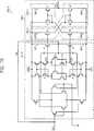
Die
Eine Mehrzahl von Sensoren ist in einer Matrix von Zeilen und Spalten in dem Berührungs-Anzeigefeld
Die
Die Berührungssteuerung
Der AFE
Der MCU
Der Anzeige-Treiber
Der Source-Treiber
Der Zeitablauf-Steuerlogikblock
Die
Die Sensorelektrode
Wenn eine Person mindestens einen von einer Mehrzahl von Sensoren berührt, wird eine Kapazität CSIG zwischen der Sensorelektrode
Ein senkrechtes parasitäres Element Cv wird zwischen der Sensorelektrode
Wenn das Berührungs-Anzeigefeld
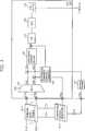
Die
Jeder der Mehrzahl von Kontakten PIN1 bis PINh ist mit jedem der Mehrzahl von Kanälen Chx1 bis Chxm und Chy1 bis Chyn gekoppelt. Eine Mehrzahl von Kanälen, zum Beispiel Chx1 bis Chxm, sind Zeilen-zugehörige Kanäle und eine Mehrzahl von Kanälen, zum Beispiel Chy1 bis Chyn sind Spalten-zugehörige Kanäle. Each of the plurality of contacts PIN1 to PINh is coupled to each of the plurality of channels Chx1 to Chxm and Chy1 to Chyn. A plurality of channels, for example, Chx1 through Chxm, are row-associated channels and a plurality of channels, for example, Chy1 through Chyn are column-associated channels.
Die Auswahlvorrichtung
Der Differenz-Abtastblock
Ein LPF
Die
Der Current Conveyor
Der Trennverstärker mit Verstärkungsfaktor Eins
Die erste Eingangsklemme IN1 und die zweite Eingangsklemme IN2 weisen die gleiche Spannung gemäß den Eigenschaften des Trennverstärkers mit Verstärkungsfaktor Eins
Der Trennverstärker mit Verstärkungsfaktor Eins
Die
Der Strom-Kopierer-Schaltkreis
Jede Größe (Länge und Breite) einer Mehrzahl von Transistoren MP1, MP2, MN1 und MN2 ist dieselbe. Ein erster Transistor MP1 und ein dritter Transistor MP2 werden durch eine erste Steuerspannung CS1 gesteuert und ein zweiter Transistor MN1 und ein vierter Transistor MN2 werden durch eine zweite Steuerspannung CS2 gesteuert. Dementsprechend ist ein in dem ersten Transistor MP1 fließender Strom IPD1 der gleiche wie ein in dem dritten Transistor MP2 fließender Strom IPD2 und ein in dem zweiten Transistor MN1 fließender Strom IND1 ist der gleiche wie ein in dem vierten Transistor MN2 fließender Strom IND2. Each size (length and width) of a plurality of transistors MP1, MP2, MN1 and MN2 is the same. A first transistor MP1 and a third transistor MP2 are controlled by a first control voltage CS1 and a second transistor MN1 and a fourth transistor MN2 are controlled by a second control voltage CS2. Accordingly, a current IPD1 flowing in the first transistor MP1 is the same as a current IPD2 flowing in the third transistor MP2, and a current IND1 flowing in the second transistor MN1 is the same as a current IND2 flowing in the fourth transistor MN2.
Ein von der ersten Eingangsklemme IN1 zu der ersten Ausgangsklemme ON1 fließender Strom SIGi ist gleich einer Differenz zwischen dem in den ersten Transistor MP1 fließenden Strom IPD1 und dem in den ersten Transistor MN1 fließenden Strom IND1. Dies kann derart ausgedrückt werden, so wie es in der Gleichung 1 dargestellt ist.A current SIGi flowing from the first input terminal IN1 to the first output terminal ON1 is equal to a difference between the current IPD1 flowing into the first transistor MP1 and the current IND1 flowing into the first transistor MN1. This can be expressed as such as shown in
[Gleichung 1][Equation 1]
SIGi = IND1 – IPD1SIGi = IND1 - IPD1
Ein Steuerstrom CC ist gleich einer Differenz zwischen einem in dem dritten Transistor MP2 fließenden Strom IPD2 und einem in dem vierten Transistor MN2 fließenden Strom IND2. Dies kann derart ausgedrückt werden, wie es in der Gleichung 2 dargestellt ist.A control current CC is equal to a difference between a current IPD2 flowing in the third transistor MP2 and a current IND2 flowing in the fourth transistor MN2. This can be expressed as shown in Equation 2.
[Gleichung 2][Equation 2]
CC = IND2 – IPD2CC = IND2 - IPD2
Durch Addieren des dritten Transistors MP2 und des vierten Transistors MN2 und Abtasten des ersten Stroms SIGi wird der abgetastete erste Strom SIGi von einem Knoten CON als ein Steuerstrom CC entnommen.By adding the third transistor MP2 and the fourth transistor MN2 and sampling the first current SIGi, the sampled first current SIGi is taken from a node CON as a control current CC.
In Bezug auf die
Der Ladungsverstärker
Wenn das Berührungs-Anzeigefeld
Die
Die Kondensator-Matrix
Der Auswahl-Bit-Generator
Der Auswahl-Bit-Generator
Wenn die Ausgangsspannung Vout größer ist als die Vergleichsspannung, zum Beispiel 0V, gibt der Komparator
Die SAR-Steuerlogik
Ein höchstwertiges Bit Q5 unter der Mehrzahl von Auswahl-Bits Q0 bis Q5 wird zum Beispiel auf „1” gesetzt und die restlichen Bits Q4 bis Q0 werden zunächst auf „0” gesetzt. Dementsprechend wird ein Schalter
Wenn ein Vergleichssignal COMP einen High-Pegel aufweist, hält die SAR-Steuerlogik
Wenn ein Vergleichssignal COMP einen Low-Pegel aufweist, setzt die SAR-Steuerlogik
Nachdem ein Schalter
Bis ein niederwertigstes Bit Q0 festgelegt ist, werden das differentielle Abtastverfahren des Differenz-Abtastblocks
Die SAR-Steuerlogik
Der Source-Treiber
Wenn eine Anzeigespannung VCOM an die gemeinsame Anzeigeelektrode
Die
Der Source-Treiber
Der Differenz-Abtastblock
Durch Durchführen eines Nichtübereinstimmungs-Kompensationsvorgangs kann sich jeder Bit-Wert der Mehrzahl von Auswahl-Bits Q0, Q1, Q2, Q3 und Q4 verändern.By performing a mismatch compensation operation, each bit value of the plurality of selection bits Q0, Q1, Q2, Q3 and Q4 may change.
Die
Der erste Strom SIGi und der zweite Strom SIGj, die in jedem der beiden Kanäle NCH und PCH fließen, tasten eine Kapazität CSIG, ein parasitäres Element Cv und ein Anzeigerauschen ab. Der Current Conveyor
Wenn das Berührungs-Anzeigefeld
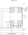
Die
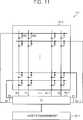
Die Sensorelektrode
Jeder der Mehrzahl von Abtast-Kanälen Y0 bis Yq, wobei q eine natürliche Zahl ist, ist mit einer Mehrzahl von in einer Spalte angeordneten Sensoren gekoppelt. Gemäß einer beispielhaften Ausführungsform kann die Mehrzahl von Abtast-Kanälen Y0 bis Yq als eine Mehrzahl von vertikalen Kanälen bezeichnet werden. Jeder Strom wird über die Mehrzahl von Abtast-Kanälen Y0 bis Yq ausgegeben. Ein gegenseitiger Kapazitäts-Knoten MC wird an einem Kreuzungspunkt von jedem der Mehrzahl von Treiber-Kanälen und jedem der Mehrzahl von Abtast-Kanälen gebildet.Each of the plurality of sampling channels Y0 to Yq, where q is a natural number, is coupled to a plurality of sensors arranged in a column. According to an exemplary embodiment, the plurality of scan channels Y0 to Yq may be referred to as a plurality of vertical channels. Each stream is output over the plurality of scan channels Y0 to Yq. A mutual capacity node MC is formed at a cross point of each of the plurality of driver channels and each of the plurality of scan channels.
Die
Ein parasitäres Element kann zwischen der Sensorelektrode
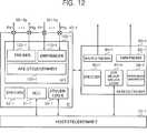
Die
Der AFE
Die AFE-Steuereinheit
Der Speicher
Der Anzeigetreiber
Jede Komponente
Die
Der AFE
Der Anzeige-Treiber
Die
Jeder der Mehrzahl von Kontakten PIN1 bis PINh ist mit jedem der Mehrzahl von Abtast-Kanälen Y0 bis Yq gekoppelt. Ein erster Strom SI1 und ein zweiter Strom SI2 werden durch die Mehrzahl von Kontakten PIN1 bis PINh empfangen. Ein erster Current Conveyor
Die
Der Trennverstärker mit Verstärkungsfaktor Eins
Jeder des ersten Stroms SIGi und des Steuerstroms CC von der
Ein zweiter Current Conveyor
Ein Ladungsverstärker
Der Ladungsverstärker
Der Empfänger
Die
Der Trennverstärker mit Verstärkungsfaktor Eins
Ähnlich zu dem ersten Strom SIGi der
[Gleichung 3][Equation 3]
SI2 = ISP1 – ISN1SI2 = ISP1 - ISN1
Der Strom ISP1 ist ein Strom, der in einem ersten Transistor P1 als Antwort auf eine erste Steuerspannung CS3 fließt und der Strom ISN1 ist ein Strom, der in einem zweiten Transistor N1 als Antwort auf eine zweite Steuerspannung CS4 fließt.The current ISP1 is a current flowing in a first transistor P1 in response to a first control voltage CS3, and the current ISN1 is a current flowing in a second transistor N1 in response to a second control voltage CS4.
Der zweite Strom-Kopierer-Schaltkreis
Ein Strom ISN4, der einen in einer Richtung des ersten Stromspiegels
Ein zweiter Steuerstrom CC2 kann wie in der Gleichung 4 dargestellt ausgedrückt werden.A second control current CC2 may be expressed as shown in Equation 4.
[Gleichung 4][Equation 4]
–CC2 = ISN4 – ISP4-CC2 = ISN4-ISP4
Eine Größe (Länge und Breite) von jedem eine Mehrzahl von Transistoren MP1, MP2, MN1 und MN2 gleicht dem anderen Punkt. Ein erster Transistor P1 und ein dritter Transistor P2 werden durch eine dritte Steuerspannung CS3 gesteuert und ein zweiter Transistor N1 und ein vierter Transistor N2 werden durch eine vierte Steuerspannung CS4 gesteuert. Dementsprechend ist eine Menge eines Stroms ISP1, der in dem ersten Transistor P1 fließt, gleich einer Menge eines Stroms ISP2, der in dem dritten Transistor P2 fließt, und eine Menge eines Stroms ISN1, die in dem zweiten Transistor N1 fließt, ist gleich einer Menge eines Stroms ISN2, die in dem vierten Transistor N2 fließt.One size (length and width) of each of a plurality of transistors MP1, MP2, MN1, and MN2 is equal to the other point. A first transistor P1 and a third transistor P2 are controlled by a third control voltage CS3, and a second transistor N1 and a fourth transistor N2 are controlled by a fourth control voltage CS4. Accordingly, an amount of a current ISP1 flowing in the first transistor P1 is equal to an amount of a current ISP2 flowing in the third transistor P2, and an amount of a current ISN1 flowing in the second transistor N1 is equal to an amount a current ISN2 flowing in the fourth transistor N2.
Eine Menge eines Stroms ISN4 ist gleich einer Menge eines Stroms ISP2 und eine Menge eines Stroms ISP4 ist gleich einer Menge eines Stroms ISN2 gemäß einer Stromspiegelung. Daher ist eine Menge eines Stroms ISN4 gleich einer Menge eines Stroms ISP1 und eine Menge eines Stroms ISP4 ist gleich einer Menge eines Stroms ISN1. An amount of a current ISN4 is equal to an amount of a current ISP2, and an amount of a current ISP4 is equal to an amount of a current ISN2 according to a current mirroring. Therefore, an amount of a current ISN4 is equal to an amount of a current ISP1, and an amount of a current ISP4 is equal to an amount of a current ISN1.
Bei dem Verbinden einer Mehrzahl von Stromspiegeln
Die
Der erste Current Conveyor
Der Ladungsverstärker
Eine Berührungssteuerung gemäß einer beispielhaften Ausführungsform der erfinderischen Idee, ein Betriebsverfahren davon und Vorrichtungen mit demselben können ein Anzeigerauschen beseitigen, das bei einer gemeinsamen Anzeigeelektrode aufgetreten ist durch differentielles Abtasten zweier von einer Mehrzahl von Kanälen. Darüber hinaus kann die Berührungssteuerung gemäß einer beispielhaften Ausführungsform der erfinderischen Idee, das Betriebsverfahren davon und die Vorrichtungen mit denselben ein Rauschen durch Kompensieren einer Nichtübereinstimmung zwischen parasitären Elementen beseitigen, das durch Nichtübereinstimmung zwischen parasitären Elementen auftrat.A touch controller according to an exemplary embodiment of the inventive concept, an operating method thereof and devices having the same can eliminate display noise that has occurred at a common display electrode by differential scanning two of a plurality of channels. Moreover, according to an exemplary embodiment of the inventive concept, the method of operation thereof, and the devices with the same, the touch controller can eliminate noise by compensating for a mismatch between parasitic elements caused by disagreement between parasitic elements.
Während beispielhafte Ausführungsformen insbesondere in Bezug auf Ausführungen davon dargestellt und beschrieben worden sind, ist es für Durchschnittsfachleute selbstverständlich, dass unterschiedliche Veränderungen der Formen und Details davon durchgeführt werden können, ohne von dem Geist und Umfang abzuweichen, so wie es durch die folgenden Ansprüche definiert ist.While exemplary embodiments have been particularly shown and described with respect to embodiments thereof, it will be understood by those of ordinary skill in the art that various changes in forms and details thereof may be made without departing from the spirit and scope as defined by the following claims ,
ZITATE ENTHALTEN IN DER BESCHREIBUNG QUOTES INCLUDE IN THE DESCRIPTION
Diese Liste der vom Anmelder aufgeführten Dokumente wurde automatisiert erzeugt und ist ausschließlich zur besseren Information des Lesers aufgenommen. Die Liste ist nicht Bestandteil der deutschen Patent- bzw. Gebrauchsmusteranmeldung. Das DPMA übernimmt keinerlei Haftung für etwaige Fehler oder Auslassungen.This list of the documents listed by the applicant has been generated automatically and is included solely for the better information of the reader. The list is not part of the German patent or utility model application. The DPMA assumes no liability for any errors or omissions.
Zitierte PatentliteraturCited patent literature
- KR 10-2012-0051060[0001]KR 10-2012-0051060[0001]
- US 7652538[0079]US 7652538[0079]
Claims (29)
Translated fromGermanApplications Claiming Priority (4)
| Application Number | Priority Date | Filing Date | Title |
|---|---|---|---|
| US201161532697P | 2011-09-09 | 2011-09-09 | |
| US61/532,697 | 2011-09-09 | ||
| KR10-2012-0051060 | 2012-05-14 | ||
| KR1020120051060AKR101961325B1 (en) | 2011-09-09 | 2012-05-14 | Touch controller, method thereof, and devices having the touch controller |
Publications (1)
| Publication Number | Publication Date |
|---|---|
| DE102012108097A1true DE102012108097A1 (en) | 2013-03-14 |
Family
ID=47740315
Family Applications (1)
| Application Number | Title | Priority Date | Filing Date |
|---|---|---|---|
| DE102012108097APendingDE102012108097A1 (en) | 2011-09-09 | 2012-08-31 | Touch controls, methods thereof, and touch control devices |
Country Status (3)
| Country | Link |
|---|---|
| US (1) | US9195353B2 (en) |
| CN (1) | CN102999210B (en) |
| DE (1) | DE102012108097A1 (en) |
Families Citing this family (34)
| Publication number | Priority date | Publication date | Assignee | Title |
|---|---|---|---|---|
| US8610443B1 (en) | 2013-03-12 | 2013-12-17 | Cypress Semiconductor Corp. | Attenuator circuit of a capacitance-sensing circuit |
| CN103186307B (en) | 2013-03-26 | 2015-10-14 | 合肥京东方光电科技有限公司 | A kind of capacitance type in-cell touch panel and display device |
| US8928359B2 (en) | 2013-05-08 | 2015-01-06 | Synaptics Incorporated | Charge distribution |
| UA84754U (en)* | 2013-06-04 | 2013-10-25 | Бетмор Кепитал Лтд | Touch-sensitive strip for electronic device control |
| CN103294322B (en)* | 2013-06-06 | 2017-07-07 | 敦泰电子有限公司 | Touch control display apparatus |
| KR20150042366A (en)* | 2013-10-10 | 2015-04-21 | 삼성전자주식회사 | Touch screen sensror integrated circuit, method thereof, and system having the same |
| US9541588B2 (en) | 2013-10-30 | 2017-01-10 | Synaptics Incorporated | Current-mode coarse-baseline-correction |
| US9170693B2 (en)* | 2013-11-21 | 2015-10-27 | Pixart Imaging Inc. | Capacitive touch system and gain control method thereof |
| US20160370411A1 (en)* | 2014-02-28 | 2016-12-22 | Azoteq (Pty) Ltd | Charge transfer measurement techniques |
| KR102249651B1 (en)* | 2014-07-23 | 2021-05-10 | 주식회사 실리콘웍스 | Touch panel sensing apparatus and controlling apparatus thereof |
| US9891763B2 (en) | 2014-09-30 | 2018-02-13 | Synaptics Incorporated | Current feedback techniques for capacitive sensing |
| US9778804B2 (en) | 2015-06-04 | 2017-10-03 | Synaptics Incorporated | Calibrating charge mismatch in a baseline correction circuit |
| US10039526B2 (en) | 2015-09-17 | 2018-08-07 | Qualcomm Incorporated | Pixel receiver with low frequency noise reduction for ultrasonic imaging apparatus |
| US10061437B2 (en)* | 2015-09-30 | 2018-08-28 | Synaptics Incorporated | Active canceling of display noise in simultaneous display and touch sensing using an impulse response |
| US9817509B2 (en)* | 2015-10-30 | 2017-11-14 | Solomon Systech Limited | Methods and apparatuses for providing sensing signals for projected capacitive touch sensing using a differential current mode analog circuit |
| US10120512B2 (en) | 2016-04-08 | 2018-11-06 | Microsoft Technology Licensing, Llc | Hover sensor |
| US20180157367A1 (en)* | 2016-12-02 | 2018-06-07 | Stmicroelectronics Asia Pacific Pte Ltd | Analog self capacitance sensing front end utilizing current conveyors |
| KR102847503B1 (en)* | 2016-12-21 | 2025-08-20 | 에스케이하이닉스 주식회사 | Capacitance sensing circuits |
| IT201700034042A1 (en)* | 2017-03-28 | 2018-09-28 | St Microelectronics Srl | CURRENT CONVEYOR DIFFERENTIAL CIRCUIT, DEVICE, EQUIPMENT AND CORRESPONDING PROCEDURE |
| US10268298B2 (en)* | 2017-05-07 | 2019-04-23 | Superc-Touch Corporation | Mutual-capacitance touch apparatus and highly sensitive mutual-capacitance touch sensing method for the same |
| US10268297B2 (en)* | 2017-05-07 | 2019-04-23 | Superc-Touch Corporation | Mutual-capacitance organic light emitting touch display apparatus |
| CN106990873B (en) | 2017-06-08 | 2019-06-21 | 京东方科技集团股份有限公司 | Touch reading circuit, touch display panel and display device |
| US10503319B2 (en)* | 2017-12-27 | 2019-12-10 | Novatek Microelectronics Corp. | Signal processing circuit for processing sensing signal from touch panel |
| US11054942B2 (en)* | 2018-04-05 | 2021-07-06 | Synaptics Incorporated | Noise suppression circuit |
| JP6703794B2 (en) | 2018-06-29 | 2020-06-03 | 双葉電子工業株式会社 | Touch panel drive device, touch panel device, touch panel drive method |
| JP2020086743A (en)* | 2018-11-21 | 2020-06-04 | ローム株式会社 | Touch detection circuit, input device, and electronic device |
| KR102817370B1 (en)* | 2018-12-27 | 2025-06-10 | 주식회사 엘엑스세미콘 | Touch Sensing Device and Display Device Including The Same |
| TWI709886B (en)* | 2019-05-02 | 2020-11-11 | 友達光電股份有限公司 | Touch and display device |
| KR102646183B1 (en)* | 2019-12-26 | 2024-03-11 | 엘지디스플레이 주식회사 | Touch display device, data driving circuit, and touch sensing method |
| US11106317B1 (en)* | 2020-04-14 | 2021-08-31 | Synaptics Incorporated | Common mode noise suppression with restoration of common mode signal |
| US11914820B2 (en)* | 2020-04-14 | 2024-02-27 | Synaptics Incorporated | Distributed analog display noise suppression circuit |
| KR102813449B1 (en) | 2020-08-06 | 2025-05-27 | 삼성전자주식회사 | A touch sensor, and a touch sensing method |
| KR20220067920A (en) | 2020-11-18 | 2022-05-25 | 삼성전자주식회사 | Touch controller, touch screen driving circuit comprising thereof and operating methof of touch screen driving circuit |
| CN119847370B (en)* | 2025-03-18 | 2025-06-17 | 上海海栎创科技股份有限公司 | A charge distribution compensation circuit and method based on touch sensing channel |
Citations (2)
| Publication number | Priority date | Publication date | Assignee | Title |
|---|---|---|---|---|
| US7652538B2 (en) | 2004-09-24 | 2010-01-26 | Samsung Electronics Co., Ltd. | Circuits and methods for improving slew rate of differential amplifiers |
| KR20120051060A (en) | 2009-07-29 | 2012-05-21 | 티슈 제네시스, 아이엔씨. | Adipose-derived stromal cells (asc) as delivery tool for treatment of cancer |
Family Cites Families (9)
| Publication number | Priority date | Publication date | Assignee | Title |
|---|---|---|---|---|
| US7663607B2 (en) | 2004-05-06 | 2010-02-16 | Apple Inc. | Multipoint touchscreen |
| US8279180B2 (en) | 2006-05-02 | 2012-10-02 | Apple Inc. | Multipoint touch surface controller |
| TWI420374B (en)* | 2008-09-08 | 2013-12-21 | Innolux Corp | Sensing circuit for capacitive touch panel and electronic device using the same |
| US9927924B2 (en)* | 2008-09-26 | 2018-03-27 | Apple Inc. | Differential sensing for a touch panel |
| JP2010108501A (en) | 2008-10-30 | 2010-05-13 | Samsung Electronics Co Ltd | Touch screen controller having increased sensing sensitivity, and display driving circuit and display device and system having the touch screen controller |
| KR101657215B1 (en)* | 2009-09-08 | 2016-09-19 | 삼성디스플레이 주식회사 | Display device including touch panel device and coupling-noise elliminating method |
| CN102043503B (en)* | 2009-10-23 | 2012-06-27 | 奇景光电股份有限公司 | Touch panel reader and multi-channel reader |
| KR20110091380A (en) | 2010-02-05 | 2011-08-11 | 삼성전자주식회사 | Noise compensation method and device of touch panel |
| US8729913B2 (en)* | 2010-08-24 | 2014-05-20 | Cypress Semiconductor Corporation | Capacitance sensing systems, circuits and methods that include current conveyor based oscillators |
- 2012
- 2012-08-31DEDE102012108097Apatent/DE102012108097A1/enactivePending
- 2012-09-06USUS13/605,247patent/US9195353B2/enactiveActive
- 2012-09-10CNCN201210333416.6Apatent/CN102999210B/enactiveActive
Patent Citations (2)
| Publication number | Priority date | Publication date | Assignee | Title |
|---|---|---|---|---|
| US7652538B2 (en) | 2004-09-24 | 2010-01-26 | Samsung Electronics Co., Ltd. | Circuits and methods for improving slew rate of differential amplifiers |
| KR20120051060A (en) | 2009-07-29 | 2012-05-21 | 티슈 제네시스, 아이엔씨. | Adipose-derived stromal cells (asc) as delivery tool for treatment of cancer |
Also Published As
| Publication number | Publication date |
|---|---|
| CN102999210B (en) | 2017-04-12 |
| CN102999210A (en) | 2013-03-27 |
| US20130063395A1 (en) | 2013-03-14 |
| US9195353B2 (en) | 2015-11-24 |
Similar Documents
| Publication | Publication Date | Title |
|---|---|---|
| DE102012108097A1 (en) | Touch controls, methods thereof, and touch control devices | |
| DE112019000251B4 (en) | TWO-ELECTRODE TOUCH BUTTON WITH A MULTI-PHASE CAPACITY MEASUREMENT PROCESS | |
| DE69425551T2 (en) | Portable computing device controlled by a sensitive mini-tablet | |
| US10095910B2 (en) | Fingerprint identification circuit, touch apparatus and fingerprint identification method | |
| TWI604344B (en) | Touch controllers, methods thereof, and devices having the touch controllers | |
| DE102011085464A1 (en) | Capacitive touchscreen system for electronic device has gain capacitor, which accumulates charge representative of capacitances in sense electrode during first stage and transfers charge to feedback capacitor during second stage | |
| DE102011007169A1 (en) | Multichip touch screen | |
| DE112018005065T5 (en) | SUPPRESSING NOISE IN TOUCH AREAS USING A SHIELDING LAYER | |
| DE112013005869T5 (en) | scanning | |
| DE102011017469A1 (en) | System and method for transferring charge for converting capacitance into voltage for touchscreen controllers | |
| DE102011085528A1 (en) | Capacitive touch screen system with touch or object position coding during analog-to-digital conversion | |
| DE102014212094A1 (en) | Pseudo-driven shielding | |
| DE102009046177A1 (en) | Touch data generator | |
| DE112015005732T5 (en) | Capacitive fingerprint sensor with sensing elements having a timing circuit | |
| DE102014209839B4 (en) | Touch pad and button detection method for this | |
| DE112014007233T5 (en) | Touch control substrate, terminal, and method of improving touch accuracy | |
| DE102017208675A1 (en) | Compensation circuit for touch sensors | |
| DE102012213691B4 (en) | Analog to digital converters with dual integrating capacitor systems | |
| DE112018004934T5 (en) | NANO PERFORMANCE CAPACITY DIGITAL CONVERTER | |
| KR101829647B1 (en) | Touch panel calibration system | |
| DE102012213752A1 (en) | Cancellation of a parasitic capacitance in a sensor interface | |
| DE112018002609T5 (en) | TECHNOLOGY FOR CANCELING UNWANTED CAPACITIVE EFFECTS IN A CAPACITIVE TOUCH INTERFACE AND RELATED SYSTEMS, METHODS AND DEVICES | |
| DE112017006270T5 (en) | CAPACITIVE CAPTURE WITH MULTIMEDIA SENSING | |
| DE112019003101T5 (en) | PARALLEL DETECTION AND MEASUREMENT OF CAPACITIVE SENSOR CHANNELS AND RELATED SYSTEMS, METHODS, AND DEVICES | |
| DE112021001212T5 (en) | Enhanced charge cancellation in a touch sensor and related systems, methods, and devices |
Legal Events
| Date | Code | Title | Description |
|---|---|---|---|
| R082 | Change of representative | Representative=s name:KUHNEN & WACKER PATENT- UND RECHTSANWALTSBUERO, DE | |
| R012 | Request for examination validly filed |