DE102011008261A1 - Rail for the electrical contacting of an electrically conductive substrate - Google Patents
Rail for the electrical contacting of an electrically conductive substrateDownload PDFInfo
- Publication number
- DE102011008261A1 DE102011008261A1DE102011008261ADE102011008261ADE102011008261A1DE 102011008261 A1DE102011008261 A1DE 102011008261A1DE 102011008261 ADE102011008261 ADE 102011008261ADE 102011008261 ADE102011008261 ADE 102011008261ADE 102011008261 A1DE102011008261 A1DE 102011008261A1
- Authority
- DE
- Germany
- Prior art keywords
- rail
- contact fingers
- contact
- electrically conductive
- solar cell
- Prior art date
- Legal status (The legal status is an assumption and is not a legal conclusion. Google has not performed a legal analysis and makes no representation as to the accuracy of the status listed.)
- Ceased
Links
Images


Classifications
- H—ELECTRICITY
- H02—GENERATION; CONVERSION OR DISTRIBUTION OF ELECTRIC POWER
- H02G—INSTALLATION OF ELECTRIC CABLES OR LINES, OR OF COMBINED OPTICAL AND ELECTRIC CABLES OR LINES
- H02G5/00—Installations of bus-bars
- H02G5/02—Open installations
- G—PHYSICS
- G01—MEASURING; TESTING
- G01R—MEASURING ELECTRIC VARIABLES; MEASURING MAGNETIC VARIABLES
- G01R1/00—Details of instruments or arrangements of the types included in groups G01R5/00 - G01R13/00 and G01R31/00
- G01R1/02—General constructional details
- G01R1/06—Measuring leads; Measuring probes
- G01R1/067—Measuring probes
- G01R1/073—Multiple probes
- G01R1/07307—Multiple probes with individual probe elements, e.g. needles, cantilever beams or bump contacts, fixed in relation to each other, e.g. bed of nails fixture or probe card
- G01R1/07342—Multiple probes with individual probe elements, e.g. needles, cantilever beams or bump contacts, fixed in relation to each other, e.g. bed of nails fixture or probe card the body of the probe being at an angle other than perpendicular to test object, e.g. probe card
- H—ELECTRICITY
- H02—GENERATION; CONVERSION OR DISTRIBUTION OF ELECTRIC POWER
- H02S—GENERATION OF ELECTRIC POWER BY CONVERSION OF INFRARED RADIATION, VISIBLE LIGHT OR ULTRAVIOLET LIGHT, e.g. USING PHOTOVOLTAIC [PV] MODULES
- H02S50/00—Monitoring or testing of PV systems, e.g. load balancing or fault identification
- H02S50/10—Testing of PV devices, e.g. of PV modules or single PV cells
- Y—GENERAL TAGGING OF NEW TECHNOLOGICAL DEVELOPMENTS; GENERAL TAGGING OF CROSS-SECTIONAL TECHNOLOGIES SPANNING OVER SEVERAL SECTIONS OF THE IPC; TECHNICAL SUBJECTS COVERED BY FORMER USPC CROSS-REFERENCE ART COLLECTIONS [XRACs] AND DIGESTS
- Y02—TECHNOLOGIES OR APPLICATIONS FOR MITIGATION OR ADAPTATION AGAINST CLIMATE CHANGE
- Y02E—REDUCTION OF GREENHOUSE GAS [GHG] EMISSIONS, RELATED TO ENERGY GENERATION, TRANSMISSION OR DISTRIBUTION
- Y02E10/00—Energy generation through renewable energy sources
- Y02E10/50—Photovoltaic [PV] energy
- Y—GENERAL TAGGING OF NEW TECHNOLOGICAL DEVELOPMENTS; GENERAL TAGGING OF CROSS-SECTIONAL TECHNOLOGIES SPANNING OVER SEVERAL SECTIONS OF THE IPC; TECHNICAL SUBJECTS COVERED BY FORMER USPC CROSS-REFERENCE ART COLLECTIONS [XRACs] AND DIGESTS
- Y10—TECHNICAL SUBJECTS COVERED BY FORMER USPC
- Y10T—TECHNICAL SUBJECTS COVERED BY FORMER US CLASSIFICATION
- Y10T29/00—Metal working
- Y10T29/49—Method of mechanical manufacture
- Y10T29/49002—Electrical device making
- Y10T29/49117—Conductor or circuit manufacturing
Landscapes
- Physics & Mathematics (AREA)
- General Physics & Mathematics (AREA)
- Measuring Leads Or Probes (AREA)
- Photovoltaic Devices (AREA)
Abstract
Translated fromGermanDescription
Translated fromGermanDie vorliegende Erfindung betrifft eine Schiene für die elektrische Kontaktierung eines elektrisch leitfähigen Substrates in Form eines dünnen, elektrisch leitenden und federnden Kontakts. Die Schiene umfasst eine Stromsammelschiene, an die eine Mehrzahl von Kontaktfingern angebracht ist. Die Erfindung zeichnet sich dadurch aus, dass die Kontaktfinger in Richtung des herzustellenden Kontaktes federnd ausgestaltet sind.The present invention relates to a rail for the electrical contacting of an electrically conductive substrate in the form of a thin, electrically conductive and resilient contact. The rail includes a bus bar to which a plurality of contact fingers are attached. The invention is characterized in that the contact fingers are designed to be resilient in the direction of the contact to be produced.
Zur Vermessung von Solarzellen ohne Zellverbinder müssen die Busbars oder Kontaktpads elektrisch durch Andruck oder Unterdruck kontaktiert werden. So kann die Zelle geflasht oder ihre Lumineszenz untersucht werden. Dies sind wichtige Verfahren für die qualitative und quantitative Bewertung von Solarzellen.To measure solar cells without cell connectors, the busbars or contact pads must be electrically contacted by pressure or negative pressure. This allows the cell to be flashed or its luminescence to be studied. These are important methods for the qualitative and quantitative evaluation of solar cells.
Bisher wurde dieses Problem über gefederte Kontaktstifte gelöst. Hersteller dieser sind z. B. Ingun Prüfmittelbau GmbH oder Tekon Prüftechnik GmbH.So far, this problem has been solved by spring-loaded pins. Manufacturer of these are z. Ingun Prüfmittelbau GmbH or Tekon Prüftechnik GmbH.
In
Derartige Kontaktstifte werden zur elektrischen Kontaktierung von beispielsweise Solarzellen eingesetzt, um beispielsweise über Flasher-Messungen (Flasher) bzw. Photo- oder Elektrolumineszenz-Messungen bestimmte Parameter dieser Solarzellen zu ermitteln. Dabei werden die Solarzellen beispielsweise über ihre Busbars mit den Kontaktstiften elektrisch kontaktiert. Typische Busbar-Breiten liegen dabei zwischen 1,5 und 2,4 mm. Aufgrund ihrer Bauart verdecken derartige Kontaktstifte entlang des Busbars allerdings aufgrund ihrer Breite einen Teil der Solarzelle, so dass es bei den im Voranstehenden beschriebenen Prüfmethoden z. T. zur Verfälschung der erhaltenen Messwerte bzw. Ergebnisse kommt.Such contact pins are used for electrical contacting of, for example, solar cells in order to determine, for example, via flasher measurements (flasher) or photo or electroluminescence measurements, certain parameters of these solar cells. The solar cells are electrically contacted, for example, via their busbars with the contact pins. Typical busbar widths are between 1.5 and 2.4 mm. Due to their design, such contact pins along the busbar but due to their width cover part of the solar cell, so that it is in the test methods described in the foregoing z. T. to the falsification of the obtained measurements or results comes.
Aus der
Die
Auch aus der
Ausgehend hiervon ist es daher Aufgabe der vorliegenden Erfindung, eine Schiene zur temporären Kontaktierung von beispielsweise Solarzellen anzugeben, mit der sich die oben genannten Nachteile vermeiden lassen.Proceeding from this, it is therefore an object of the present invention to provide a rail for the temporary contacting of, for example, solar cells, with which the above-mentioned disadvantages can be avoided.
Diese Aufgabe wird bezüglich der Schiene mit den Merkmalen des Patentanspruchs 1, bezüglich des Herstellungsverfahrens der Schiene mit den Merkmalen des Patentanspruchs 15 sowie bezüglich eines Überprüfungsverfahrens einer Solarzelle mit den Merkmalen des Patentanspruchs 16 gelöst. Die jeweiligen abhängigen Patentansprüche stellen dabei vorteilhafte Weiterbildungen dar.This object is achieved with respect to the rail with the features of
Erfindungsgemäß wird somit eine Schiene für die elektrische Kontaktierung eines elektrisch leitfähigen Substrates bereitgestellt, die eine in x-Richtung länglich ausgebildete und in y-Richtung eine gewisse Dicke aufweisende Stromsammelschiene umfasst, die eine Mehrzahl von einseitig an der Stromsammelschiene angeordneten Kontaktfingern, die eine Richtungskomponente in Richtung der herzustellenden Kontaktierung (z-Richtung) aufweisen, wobei die Stromsammelschiene und die Kontaktfinger einstückig ausgebildet sind. Erfindungswesentlich dabei ist, dass die Kontaktfinger in z-Richtung federnd ausgestaltet sind. According to the invention, a rail for the electrical contacting of an electrically conductive substrate is thus provided, which has a longitudinally formed in the x-direction and in the y-direction of a certain thickness busbar comprising a plurality of unilaterally arranged on the busbar contact fingers, a directional component in Direction of the contact (z-direction) to be produced, wherein the current busbar and the contact fingers are integrally formed. Essential to the invention is that the contact fingers are resilient in the z direction.
Die erfindungsgemäße Lösung umfasst somit eine Schiene, die prinzipiell in zwei funktionelle Einheiten aufgeteilt ist, nämlich eine Stromsammelschiene, die bevorzugt durchgehend ausgebildet ist, sowie einseitig von dieser Stromsammelschiene ausgehende Kontaktfinger, die mit der Stromsammelschiene elektrisch verbunden sind. Die Stromsammelschiene dient nicht nur zur Stromführung, sondern zusätzlich zur mechanischen Stabilisierung der Kontaktschiene gegen Kräfte von außen. Die erfindungsgemäße Schiene weist dabei eine Dimensionierung auf, in der die Schiene länglich ausgebildet ist (x-Richtung); die Tiefe oder Dicke der Stromsammelschiene ist als y-Richtung definiert. Die Richtung, in der eine Kontaktierung der Schiene mit einem Substrat, beispielsweise einer Solarzelle, erfolgen soll (und in der die Kontaktfinger von der Stromsammelschiene abzweigen) ist als z-Richtung definiert. Erfindungswesentlich ist nun, dass jeder der Kontaktfinger derart ausgestaltet ist, dass eine Federwirkung in z-Richtung gegeben ist, so dass bei Kontaktierung der Schiene mit einem zu kontaktierenden Substrat, z. B. indem die Schiene in z-Richtung mit den Kontaktfingern über die Spitzen der Kontaktfinger mit dem zu kontaktierenden Substrat in Berührung gebracht wird, eine Abfederung und dadurch Reduzierung der wirkenden Anpresskraft gegeben ist.The solution according to the invention thus comprises a rail, which is in principle divided into two functional units, namely a current bus, which is preferably formed continuously, as well as one side of this busbar outgoing contact fingers, which are electrically connected to the power bus. The busbar serves not only to conduct electricity, but in addition to the mechanical stabilization of the contact rail against external forces. The rail according to the invention in this case has a dimensioning in which the rail is elongated (x-direction); the depth or thickness of the bus bar is defined as the y direction. The direction in which a contacting of the rail with a substrate, for example a solar cell, should take place (and in which the contact fingers branch off from the busbar) is defined as the z-direction. Is essential to the invention now that each of the contact fingers is designed such that a spring action in the z-direction is given, so that when contacting the rail with a substrate to be contacted, for. B. by the rail is brought into contact with the contact fingers on the tips of the contact fingers with the substrate to be contacted in the z-direction, a cushioning and thereby reducing the acting contact pressure is given.
Dies hat einerseits den Vorteil, dass eine Vielzahl von Kontaktpunkten auf der Solarzelle selbst hergestellt werden kann. Andererseits kann durch die Federwirkung eines jeden Kontaktes einer übermäßigen Krafteinwirkung auf die Solarzellenoberfläche und somit einer Beschädigung oder gar Zerstörung der Solarzelle nachhaltig entgegen gewirkt werden. Weiter hat es sich als vorteilhaft erwiesen, dass insbesondere für den Fall, dass die Schiene eine äußerst geringe Dimensionierung in y-Richtung, d. h. eine geringe Dicke, aufweist, eine großflächige Abschattung der Solarzelle vermieden werden kann. Somit ist ein im Wesentlichen ungestörter Lichteinfall auf die Solarzelle (in z-Richtung), aber auch, z. B. für den Fall einer Photo- bzw. Elektro-Lumineszenz-Messung, eine weitgehend ungehinderte Lichtemission (ebenso in z-Richtung) aus der Solarzelle gewährleistet.On the one hand, this has the advantage that a multiplicity of contact points can be produced on the solar cell itself. On the other hand, by the spring action of each contact an excessive force on the solar cell surface and thus damage or even destruction of the solar cell can be permanently counteracted. Furthermore, it has proved to be advantageous, in particular in the case where the rail has an extremely small dimensioning in the y-direction, ie. H. has a small thickness, a large-scale shading of the solar cell can be avoided. Thus, a substantially undisturbed incidence of light on the solar cell (in the z-direction), but also, for. B. in the case of a photo- or electro-luminescence measurement, a largely unimpeded light emission (as well in the z-direction) ensured from the solar cell.
Im Gegensatz zur aus der zuvor zitierten
Besonders bevorzugte Ausführungsformen der erfindungsgemäßen Schiene werden nachfolgend beschrieben.Particularly preferred embodiments of the rail according to the invention are described below.
Vorteilhaft ist beispielsweise, wenn die federnde Ausgestaltung der Kontaktfinger dadurch bedingt ist, dass der Winkel, der zwischen der x-Richtung und dem Verlauf der Kontaktfinger ausgebildet ist, zwischen 10° und 70°, bevorzugt zwischen 15° und 50°, weiter bevorzugt zwischen 20 und 40°, besonders bevorzugt zwischen 25° und 35° beträgt. Gemäß dieser Ausführungsform sind die Kontaktfinger abgewinkelt bezüglich der Stromsammelschiene angebracht. Die Abwinklung erfolgt jedoch dabei in der x-/z-Richtung, so dass der Verlauf der Kontaktfinger in z-Richtung im Wesentlichen vollständig bzw. vollständig von der Stromsammelschiene verdeckt ist. In Projektion in z-Richtung ist die Schiene daher ebenso sehr dünn ausgebildet. Beim Andrücken in z-Richtung der Schiene auf das zu kontaktierende Substrat erfolgt durch die abgewinkelte Anordnung der Kontaktfinger ein weiteres Abknicken der Kontaktfinger, wodurch die Federwirkung gegeben ist.It is advantageous, for example, if the resilient configuration of the contact fingers is due to the fact that the angle formed between the x-direction and the course of the contact fingers is between 10 ° and 70 °, preferably between 15 ° and 50 °, more preferably between 20 and 40 °, more preferably between 25 ° and 35 °. According to this embodiment, the contact fingers are angled relative to the bus bar mounted. However, the angling takes place in the x- / z-direction, so that the course of the contact fingers in the z-direction is substantially completely or completely covered by the current busbar. In projection in the z-direction, the rail is therefore also very thin. When pressing in the z-direction of the rail on the substrate to be contacted by the angled arrangement of the contact fingers a further bending of the contact fingers, whereby the spring action is given.
Alternativ oder zusätzlich hierzu kann die federnde Ausgestaltung der Kontaktfinger dadurch erfolgen, dass die Kontaktfinger einen nicht geradlinigen Verlauf, insbesondere einen geschwungenen oder bogenförmigen Verlauf, aufweisen.Alternatively or additionally, the resilient configuration of the contact fingers can be effected in that the contact fingers have a non-straight course, in particular a curved or curved course.
Gemäß dieser Ausführungsform ist vorgesehen, dass durch einen nicht geradlinigen Verlauf der Kontaktfinger die Federwirkung erfolgen kann. In einer besonders bevorzugten Ausführungsform ist der geschwungene oder bogenförmige Verlauf der Kontaktfinger derart ausgebildet, dass die Kontaktfinger in Projektion in z-Richtung ebenso von der Stromsammelschiene verdeckt werden, d. h. der geschwungene oder bogenförmige Verlauf der Kontaktfinger in der x-/z-Ebene der Schiene festgelegt ist.According to this embodiment, it is provided that the spring effect can be achieved by a non-linear course of the contact fingers. In a particularly preferred embodiment, the curved or curved course of the contact fingers is designed such that the contact fingers are also hidden in projection in the z-direction of the power bus, d. H. the curved or arcuate course of the contact fingers in the x- / z-plane of the rail is fixed.
Vorteilhaft ist weiterhin, wenn die Spitzen der Kontaktfinger abgerundet und/oder abgeflacht ausgestaltet sind. Durch eine Abrundung der Spitzen kann ein flächigerer Kontakt gewährleistet werden und somit der Kontaktwiderstand reduziert werden.It is also advantageous if the tips of the contact fingers rounded and / or flattened are designed. By rounding the tips, a surface contact can be ensured and thus the contact resistance can be reduced.
Zudem ist gemäß einer weiteren vorteilhaften Ausführungsform vorgesehen, dass die Kontaktfinger parallel und/oder äquidistant angeordnet sind.In addition, it is provided according to a further advantageous embodiment that the contact fingers are arranged parallel and / or equidistant.
Bevorzugt ist ebenso, wenn der Abstand der Kontaktfinger zueinander weniger als 2 mm, bevorzugt weniger als 1 mm, besonders bevorzugt zwischen 0,05 und 0,5 mm, insbesondere zwischen 0,12 und 0,15 mm beträgt.It is also preferred if the distance of the contact fingers to one another is less than 2 mm, preferably less than 1 mm, particularly preferably between 0.05 and 0.5 mm, in particular between 0.12 and 0.15 mm.
Weiterhin ist vorteilhaft, wenn die Länge aller Kontaktfinger gleich ist.Furthermore, it is advantageous if the length of all contact fingers is the same.
In einer weiteren vorteilhaften Ausführungsform beträgt
- a) die Länge der Kontaktfinger zwischen 10 und 50 mm, bevorzugt zwischen 15 und 30 mm, besonders bevorzugt zwischen 20 und 25 mm und/oder
- b) die Breite der Kontaktfinger in x-Richtung zwischen 0,05 und 2,0 mm, bevorzugt zwischen 0,1 und 1,0 mm, besonders bevorzugt zwischen 0,15 und 0,6 mm.
- a) the length of the contact fingers between 10 and 50 mm, preferably between 15 and 30 mm, more preferably between 20 and 25 mm and / or
- b) the width of the contact fingers in the x direction between 0.05 and 2.0 mm, preferably between 0.1 and 1.0 mm, more preferably between 0.15 and 0.6 mm.
Bevorzugt ist weiterhin, wenn die Schiene sehr schmal ausgebildet ist, d. h. dass die Stromsammelschiene und/oder die Kontaktfinger in y-Richtung weniger als 1,0 mm, bevorzugt weniger als 0,5 mm, besonders bevorzugt zwischen 0,05 und 0,3 mm, insbesondere zwischen 0,08 und 0,15 mm dick sind. Dabei weist die Stromsammelschiene in y-Richtung bevorzugt die gleiche Dimensionierung wie die Kontaktfinger auf. Beide Bereiche der erfindungsgemäßen Schiene sind z. B. als gleich dicke Folie mit einer beispielhaften Dicke von 0,1 mm ausgebildet.Furthermore, it is preferred if the rail is very narrow, d. H. the current bus bar and / or the contact fingers in the y direction are less than 1.0 mm, preferably less than 0.5 mm, particularly preferably between 0.05 and 0.3 mm, in particular between 0.08 and 0.15 mm thick are. In this case, the current bus bar in the y direction preferably has the same dimensions as the contact fingers. Both areas of the rail according to the invention are z. B. formed as an equal thickness film with an exemplary thickness of 0.1 mm.
Eine weitere Ausgestaltung der Schiene sieht vor, dass sie über 5 bis 500, bevorzugt über 10 bis 200 Kontaktfinger umfasst.A further embodiment of the rail provides that it comprises over 5 to 500, preferably over 10 to 200, contact fingers.
Hinsichtlich der in Frage kommenden Materialien ist es vorteilhaft, wenn die Stromsammelschiene sowie die Kontaktfinger aus einem elektrisch leitfähigen Material, insbesondere einem Metall, wie z. B. Kupfer, Silber und/oder Legierungen hieraus sowie Kupfer und Beryllium enthaltende Legierungen, gebildet ist.With regard to the materials in question, it is advantageous if the busbar and the contact fingers of an electrically conductive material, in particular a metal such. As copper, silver and / or alloys thereof and copper and beryllium-containing alloys is formed.
Weiter ist es möglich, wenn zumindest die Kontaktfinger zumindest bereichsweise, insbesondere zumindest im Bereich der Kontaktstellen, eine elektrisch leitfähige Beschichtung, insbesondere eine Goldbeschichtung, aufweisen.Furthermore, it is possible if at least the contact fingers have an electrically conductive coating, in particular a gold coating, at least in regions, in particular at least in the region of the contact points.
Unter herstellungstechnischen Aspekten ist es insbesondere bevorzugt, wenn die Stromsammelschiene und die Kontaktfinger einstückig ausgebildet sind.From manufacturing-technical aspects, it is particularly preferred if the current busbar and the contact fingers are integrally formed.
Eine weitere bevorzugte Ausführungsform der vorliegenden Erfindung sieht vor, dass die Stromsammelschiene zur mechanischen Stabilisierung in y-Richtung durch mindestens eine mit der Stromsammelschiene form- und/oder kraftschlüssig verbundene elektrisch leitfähige Platte, bevorzugt durch zwei beidseitig in y-Richtung mit der Stromsammelschiene form- und/oder kraftschlüssig verbundene elektrisch leitfähige Platten, verstärkt ist. Die Verbindung der form- oder kraftschlüssig mit der Schiene verbundenen elektrischen leitfähigen Platten kann dabei zum Beispiel durch Löten, Kleben, aber auch durch mechanische Verbindungen, wie beispielsweise Schrauben oder Nieten, bewerkstelligt werden. Die Platte bzw. die Platten dienen dabei der mechanischen Verstärkung der erfindungsgemäßen Schiene, insbesondere im Bereich der Stromsammelschiene.A further preferred embodiment of the present invention provides that the current busbar for mechanical stabilization in the y direction by at least one electrically conductive plate positively and / or non-positively connected to the busbar, preferably by two on both sides in y-direction with the current busbar form- and / or non-positively connected electrically conductive plates, is reinforced. The connection of the form-fitting or non-positively connected to the rail electrical conductive plates can be accomplished, for example, by soldering, gluing, but also by mechanical connections, such as screws or rivets. The plate or the plates serve for the mechanical reinforcement of the rail according to the invention, in particular in the region of the busbar.
Dabei ist es vorteilhaft, wenn die Platte oder die Platten eine Dicke in y-Richtung zwischen 0,1 und 2 mm, bevorzugt zwischen 0,3 und 0,5 mm aufweisen. Insbesondere ist dabei die Platte oder die Platten aus dem gleichen Material wie die Schiene gebildet. Hierzu wird auf die oben genannte Materialauswahl verwiesen.It is advantageous if the plate or plates have a thickness in the y-direction between 0.1 and 2 mm, preferably between 0.3 and 0.5 mm. In particular, the plate or plates is formed from the same material as the rail. Reference is made to the above material selection.
Besonders bevorzugt ist, wenn die Schiene zumindest bereichsweise mit Ausnahme der Bereiche, die der elektrischen Kontaktierung dienen, mit einer Schutzschicht und/oder einer reflexionsreduzierenden Schicht, insbesondere einer Lackschicht, überzogen ist. Insbesondere kommen hierzu Emissionsgradlacke, beispielsweise das Fabrikat TETNAL® oder das Fabrikat SENOTHERM® der Firma InfraTech GmbH zum Einsatz.It is particularly preferred if the rail is covered with a protective layer and / or a reflection-reducing layer, in particular a lacquer layer, at least in regions, with the exception of the regions which serve for the electrical contacting. In particular, this emissivity coatings, such as the make TETNAL® or the make SENOTHERM® InfraTech GmbH are used.
Erfindungsgemäß wird ebenso ein Verfahren zur Herstellung einer im Voranstehenden beschriebenen Schiene angegeben, bei der aus einem Rohling z. B. einer Platine für die Schiene mittels eines Materialabtragsschrittes Material entfernt wird, so dass die Anordnung der Kontaktfinger entsteht. Als Rohling für die erfindungsgemäße Schiene kommt beispielsweise ein entsprechend aus einem leitfähigen Material gebildeter Materialstreifen oder eine entsprechende Platine mit einer länglichen Ausdehnung (x-Richtung), Ausdehnung in der Breite (z-Richtung) sowie einer gewissen Dicke (y-Richtung) in Frage. In dem Bereich des Rohlings, in dem die Kontaktfinger entstehen sollen, wird nun bereichsweise eine Durchtrennung des Rohlings in der x-/y-Ebene vorgenommen, so dass voneinander separierte Kontaktfinger in der x-/z-Richtung entstehen. In dem Bereich, in dem die Stromsammelschiene ausgebildet werden soll, wird der Rohling nicht bearbeitet. Es können jedoch auch in diesem Bereich zusätzliche Durchtrennungen, z. B. Bohrungen, etc., in den Materialstreifen eingebracht werden, um beispielsweise verstärkende Platten an der Stromsammelschiene zu fixieren. Alle zuvor beschriebenen bevorzugten geometrischen Ausgestaltungen der Kontaktfinger können durch das erfindungsgemäße Verfahren bewerkstelligt werden.According to the invention, a method for producing a rail described in the foregoing is also specified, in which a blank z. B. a circuit board for the rail by means of a Materialabtragsschritt material is removed, so that the arrangement of the contact fingers is formed. As a blank for the rail according to the invention is for example a correspondingly formed of a conductive material material strip or a corresponding board with an elongated extent (x-direction), expansion in width (z-direction) and a certain thickness (y-direction) in question , In the region of the blank in which the contact fingers are to be formed, a sectioning of the blank in the x- / y-plane is now carried out in regions, so that mutually separated contact fingers are formed in the x / z direction. In the area in which the busbar is to be formed, the blank is not processed. However, it is also possible in this area additional cuts, z. B. holes, etc., in the Material strips are introduced to fix, for example, reinforcing plates on the busbar. All of the previously described preferred geometric configurations of the contact fingers can be accomplished by the method according to the invention.
Der Materialabtrag kann dabei direkt erfolgen, indem beispielsweise mit entsprechenden Laserablationsverfahren oder mechanischen Materialabtragsverfahren gearbeitet wird, ebenso kann der Materialabtrag durch entsprechende Ätzverfahren erfolgen. Hierzu wird der Rohling beispielsweise mit einer entsprechenden Ätzmaske versehen, die an den Stellen, an denen der Materialabtrag erfolgen soll, ausgespart wird.The removal of material can be carried out directly, for example, by working with appropriate laser ablation or mechanical Materialabtragsverfahren, as well as the removal of material can be done by appropriate etching. For this purpose, the blank is provided for example with a corresponding etching mask, which is cut out at the locations where the material removal is to take place.
Ferner wird erfindungsgemäß ein Verfahren zur Überprüfung einer Solarzelle angegeben, bei dem eine Solarzelle mit mindestens zwei zuvor beschriebenen Schienen über die Kontaktfinger elektrisch kontaktiert wird, indem eine elektrische Kontaktierung der Busbars vorgenommen wird, und anschließend die Solarzelle geflasht und/oder zur Photolumineszenz und/oder zur Elektrolumineszenz angeregt und/oder vermessen wird. Dabei wird zumindest ein Schienenpaar zur elektrischen Kontaktierung einer Solarzelle benötigt. Die Schienen werden derart mit der Solarzelle kontaktiert, dass die Spitzen der Kontaktfinger mit dem Substrat, d. h. der Solarzelle, in Berührung gebracht werden. Bevorzugt wird die Schiene so auf der Solarzelle arrangiert, dass die Abschattung der Solarzelle durch die Schiene möglichst minimal ist.Furthermore, a method for testing a solar cell is specified according to the invention, in which a solar cell with at least two previously described rails is electrically contacted via the contact fingers by electrical contacting of the busbars, and then the solar cell is flashed and / or photoluminescence and / or is excited and / or measured for electroluminescence. In this case, at least one pair of rails is required for electrical contacting of a solar cell. The rails are contacted with the solar cell such that the tips of the contact fingers are in contact with the substrate, i. H. the solar cell, to be brought into contact. The rail is preferably arranged on the solar cell in such a way that the shadowing of the solar cell by the rail is as minimal as possible.
Bei Solarzellen, die beispielsweise zwei Busbars aufweisen, kann eine Kontaktierung der Solarzelle auch mittels dreier der erfindungsgemäßen Schienen erfolgen. Dabei kann beispielsweise jeder der zwei auf der Vorderseite vorhandenen Busbars mit jeweils einer Schiene kontaktiert werden, zusätzlich wird auch der Rückseitenkontakt der Solarzelle mit einer entsprechenden Schiene kontaktiert.In the case of solar cells having, for example, two busbars, the solar cell can also be contacted by means of three rails according to the invention. In this case, for example, each of the two busbars present on the front side can be contacted in each case with one rail, in addition the rear-side contact of the solar cell is also contacted with a corresponding rail.
Eine analoge Vorgehensweise ist ebenso für Solarzellen mit drei Busbars denkbar, auch hier kann ein jeder der Busbars mit jeweils einer Kontaktschiene kontaktiert werden.An analogous procedure is also conceivable for solar cells with three busbars, here too, each of the busbars can be contacted with one contact rail each.
Die vorliegende Erfindung wird anhand der nachfolgend dargestellten Ausführungsformen sowie der beigefügten Figur näher beschrieben, ohne die Erfindung auf die dort dargestellten speziellen Ausführungsformen zu beschränken.The present invention will be described in more detail with reference to the embodiments illustrated below and the attached figure, without limiting the invention to the specific embodiments shown there.
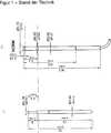
In
In
Die zuvor beschriebenen Kontaktschienen reduzieren die Messabweichung durch den seriellen Widerstand des Busbars. Weiterhin reduzieren diese die Abschattung der Zelle. Bei gleich vielen Kontaktpunkten ist eine Kontaktierung über die Kontaktschiene günstiger gegenüber einer Kontaktierung mit Kontaktstiften. Außerdem ist auf einfache Weise eine Flexibilität in der Anordnung der zellseitigen Kontaktpads zu realisieren.The contact rails described above reduce the measurement deviation due to the serial resistance of the busbar. Furthermore, these reduce the shading of the cell. For the same number of contact points a contact via the contact rail is cheaper compared to a contact with pins. In addition, a flexibility in the arrangement of the cell-side contact pads can be realized in a simple manner.
Für die Kontaktierung wird z. B. ein geätztes und elektrisch leitfähiges Material mit einer Au-Schicht verwendet. Zur mechanischen Stabilisierung dieser Folie wird dieses mit einem oder mehreren dünnen und elektrisch leitenden Blechen, bevorzugt aus demselben Werkstoff wie die Schiene, verlötet. Da diese Bleche den Querschnitt der Stromführung vergrößern, verringert sich der Spannungsabfall über der Schiene. Dadurch, dass sehr dünne Materialen verwendet werden, fällt die Kontaktierung dünner aus als herkömmliche Kontaktierungsvarianten. Ist die Kontaktierung breiter als der Busbar, wird ein Teil der Solarzelle verschattet. Dies verfälscht das Messergebnis und führt durch den Schattenwurf bei der EL zum Informationsverlust.For contacting z. B. uses an etched and electrically conductive material with an Au layer. For mechanical stabilization of this film is this with one or more thin and electrically conductive sheets, preferably of the same material as the rail soldered. As these sheets increase the cross-section of the current lead, the voltage drop across the lead is reduced. The fact that very thin materials are used, the contact is thinner than conventional Kontaktierungsvarianten. If the contact is wider than the busbar, a part of the solar cell is shaded. This falsifies the measurement result and leads to loss of information due to the shadow cast in the EL.
Mit Hilfe dieser Erfindung können Solarzellen ohne (oder mit) Zellverbinder elektrisch kontaktiert und z. B. per EL oder Flasher untersucht werden.With the aid of this invention, solar cells without (or with) cell connectors can be electrically contacted and z. B. by EL or flasher.
Neben dem Materialkostenvorteil reduziert die Kontaktschiene gegenüber herkömmlichen Kontaktierungsvarianten die Verschattung und durch die dicht liegenden Kontaktpunkte den Messfehler durch den seriellen Widerstand des Busbars.In addition to the material cost advantage, the contact rail reduces the shading compared to conventional contacting variants and the measuring error due to the close contact points due to the serial resistance of the busbar.
ZITATE ENTHALTEN IN DER BESCHREIBUNG QUOTES INCLUDE IN THE DESCRIPTION
Diese Liste der vom Anmelder aufgeführten Dokumente wurde automatisiert erzeugt und ist ausschließlich zur besseren Information des Lesers aufgenommen. Die Liste ist nicht Bestandteil der deutschen Patent- bzw. Gebrauchsmusteranmeldung. Das DPMA übernimmt keinerlei Haftung für etwaige Fehler oder Auslassungen.This list of the documents listed by the applicant has been generated automatically and is included solely for the better information of the reader. The list is not part of the German patent or utility model application. The DPMA assumes no liability for any errors or omissions.
Zitierte PatentliteraturCited patent literature
- EP 0078339[0006, 0008, 0014]EP 0078339[0006, 0008, 0014]
- US 2007/0068567 A1[0007]US 2007/0068567 A1[0007]
- DE 102008038186 A1[0008]DE 102008038186 A1[0008]
- US 2007/0068567[0014]US 2007/0068567[0014]
- DE 102008038186[0014]DE 102008038186[0014]
Zitierte Nicht-PatentliteraturCited non-patent literature
- Tekon Prüfmitteltechnik GmbH: Kontaktstifte Katalog 2009, Weinstadt[0004]Tekon Prüfmitteltechnik GmbH: Contact pins catalog 2009, Weinstadt[0004]
Claims (17)
Translated fromGermanPriority Applications (5)
| Application Number | Priority Date | Filing Date | Title |
|---|---|---|---|
| DE102011008261ADE102011008261A1 (en) | 2011-01-11 | 2011-01-11 | Rail for the electrical contacting of an electrically conductive substrate |
| US13/979,009US9444239B2 (en) | 2011-01-11 | 2012-01-03 | Bar for electronically contacting an electrically conductive substrate |
| CN2012800049337ACN103299198A (en) | 2011-01-11 | 2012-01-03 | Bar for electrically contacting an electrically conductive substrate |
| PCT/EP2012/000012WO2012095275A1 (en) | 2011-01-11 | 2012-01-03 | Bar for electrically contacting an electrically conductive substrate |
| EP12700546.0AEP2663870B1 (en) | 2011-01-11 | 2012-01-03 | Bar for electrically contacting an electrically conductive substrate |
Applications Claiming Priority (1)
| Application Number | Priority Date | Filing Date | Title |
|---|---|---|---|
| DE102011008261ADE102011008261A1 (en) | 2011-01-11 | 2011-01-11 | Rail for the electrical contacting of an electrically conductive substrate |
Publications (1)
| Publication Number | Publication Date |
|---|---|
| DE102011008261A1true DE102011008261A1 (en) | 2012-07-12 |
Family
ID=45507684
Family Applications (1)
| Application Number | Title | Priority Date | Filing Date |
|---|---|---|---|
| DE102011008261ACeasedDE102011008261A1 (en) | 2011-01-11 | 2011-01-11 | Rail for the electrical contacting of an electrically conductive substrate |
Country Status (5)
| Country | Link |
|---|---|
| US (1) | US9444239B2 (en) |
| EP (1) | EP2663870B1 (en) |
| CN (1) | CN103299198A (en) |
| DE (1) | DE102011008261A1 (en) |
| WO (1) | WO2012095275A1 (en) |
Cited By (2)
| Publication number | Priority date | Publication date | Assignee | Title |
|---|---|---|---|---|
| DE102015105975B4 (en)* | 2015-04-20 | 2019-07-11 | h.a.l.m. elektronik GmbH | Contacting device and method for measuring a characteristic of a solar cell |
| DE102018102840A1 (en)* | 2018-02-08 | 2019-08-08 | Wavelabs Solar Metrology Systems Gmbh | Device for electrical contacting of a solar cell in the measurement of electrical characteristics of the solar cell and method for measuring electrical characteristics of a solar cell |
Families Citing this family (7)
| Publication number | Priority date | Publication date | Assignee | Title |
|---|---|---|---|---|
| DE102012017564B4 (en)* | 2012-09-05 | 2018-10-11 | Universität Konstanz | Device for non-permanent electrical contacting of solar cells for measuring electrical properties |
| KR20230019226A (en) | 2014-12-30 | 2023-02-07 | 테크노프로브 에스.피.에이. | Semi-finished product comprising a plurality of contact probes for a testing head and related manufacturing method |
| US10938342B2 (en)* | 2018-04-25 | 2021-03-02 | Kyoshin Electric Co., Ltd. | Probe and solar battery cell measurement apparatus |
| JP7130247B2 (en)* | 2019-05-31 | 2022-09-05 | 共進電機株式会社 | Probes and measuring devices for solar cells |
| DE202020005915U1 (en) | 2020-04-01 | 2023-03-17 | Ingun Prüfmittelbau Gmbh | Test rail for solar cells |
| DE102020109119B4 (en)* | 2020-04-01 | 2023-05-25 | Ingun Prüfmittelbau Gmbh | Test rail for solar cells |
| DE102024101602A1 (en) | 2024-01-19 | 2025-07-24 | Ingun Prüfmittelbau Gmbh | Test element for solar cells |
Citations (7)
| Publication number | Priority date | Publication date | Assignee | Title |
|---|---|---|---|---|
| EP0078339A1 (en) | 1981-10-30 | 1983-05-11 | Ibm Deutschland Gmbh | Test apparatus for testing runs of a circuit board with at least one test head comprising a plurality of flexible contacts |
| EP0531984A1 (en)* | 1991-09-11 | 1993-03-17 | EXPORT-CONTOR Aussenhandelsgesellschaft mbH | Electronic circuit for semi-conductor power components |
| EP0588094A1 (en)* | 1992-08-19 | 1994-03-23 | Kabushiki Kaisha Toshiba | Semiconductor device with reduced internal inductance |
| US20040127073A1 (en)* | 2002-12-27 | 2004-07-01 | Ngk Insulators, Ltd. | Contact sheet, method of manufacturing the same and socket including the same |
| US20070068567A1 (en) | 2005-09-23 | 2007-03-29 | Rubin Leonid B | Testing apparatus and method for solar cells |
| DE102006006423A1 (en)* | 2006-02-13 | 2007-08-23 | Semikron Elektronik Gmbh & Co. Kg | Power semiconductor module and associated manufacturing method |
| DE102008038186A1 (en) | 2008-08-19 | 2010-02-25 | Suss Microtec Test Systems Gmbh | Probe for the temporary electrical contacting of a solar cell |
Family Cites Families (6)
| Publication number | Priority date | Publication date | Assignee | Title |
|---|---|---|---|---|
| US6628041B2 (en)* | 2000-05-16 | 2003-09-30 | Calient Networks, Inc. | Micro-electro-mechanical-system (MEMS) mirror device having large angle out of plane motion using shaped combed finger actuators and method for fabricating the same |
| US20080157793A1 (en) | 2003-02-04 | 2008-07-03 | Microfabrica Inc. | Vertical Microprobes for Contacting Electronic Components and Method for Making Such Probes |
| CN101006347A (en) | 2004-08-26 | 2007-07-25 | Sv探针私人有限公司 | Stacked tip cantilever electrical connector |
| JP4545760B2 (en)* | 2004-12-15 | 2010-09-15 | 富士通セミコンダクター株式会社 | Contact member, contactor and contact method |
| HUE050537T2 (en)* | 2006-05-05 | 2020-12-28 | Bt Imaging Pty Ltd | Method for testing indirect band gap semiconductor devices using luminescent imaging |
| DE102008038184A1 (en)* | 2008-08-19 | 2010-02-25 | Suss Microtec Test Systems Gmbh | Method and device for the temporary electrical contacting of a solar cell |
- 2011
- 2011-01-11DEDE102011008261Apatent/DE102011008261A1/ennot_activeCeased
- 2012
- 2012-01-03CNCN2012800049337Apatent/CN103299198A/enactivePending
- 2012-01-03EPEP12700546.0Apatent/EP2663870B1/enactiveActive
- 2012-01-03WOPCT/EP2012/000012patent/WO2012095275A1/enactiveApplication Filing
- 2012-01-03USUS13/979,009patent/US9444239B2/enactiveActive
Patent Citations (7)
| Publication number | Priority date | Publication date | Assignee | Title |
|---|---|---|---|---|
| EP0078339A1 (en) | 1981-10-30 | 1983-05-11 | Ibm Deutschland Gmbh | Test apparatus for testing runs of a circuit board with at least one test head comprising a plurality of flexible contacts |
| EP0531984A1 (en)* | 1991-09-11 | 1993-03-17 | EXPORT-CONTOR Aussenhandelsgesellschaft mbH | Electronic circuit for semi-conductor power components |
| EP0588094A1 (en)* | 1992-08-19 | 1994-03-23 | Kabushiki Kaisha Toshiba | Semiconductor device with reduced internal inductance |
| US20040127073A1 (en)* | 2002-12-27 | 2004-07-01 | Ngk Insulators, Ltd. | Contact sheet, method of manufacturing the same and socket including the same |
| US20070068567A1 (en) | 2005-09-23 | 2007-03-29 | Rubin Leonid B | Testing apparatus and method for solar cells |
| DE102006006423A1 (en)* | 2006-02-13 | 2007-08-23 | Semikron Elektronik Gmbh & Co. Kg | Power semiconductor module and associated manufacturing method |
| DE102008038186A1 (en) | 2008-08-19 | 2010-02-25 | Suss Microtec Test Systems Gmbh | Probe for the temporary electrical contacting of a solar cell |
Non-Patent Citations (1)
| Title |
|---|
| Tekon Prüfmitteltechnik GmbH: Kontaktstifte Katalog 2009, Weinstadt |
Cited By (3)
| Publication number | Priority date | Publication date | Assignee | Title |
|---|---|---|---|---|
| DE102015105975B4 (en)* | 2015-04-20 | 2019-07-11 | h.a.l.m. elektronik GmbH | Contacting device and method for measuring a characteristic of a solar cell |
| DE102018102840A1 (en)* | 2018-02-08 | 2019-08-08 | Wavelabs Solar Metrology Systems Gmbh | Device for electrical contacting of a solar cell in the measurement of electrical characteristics of the solar cell and method for measuring electrical characteristics of a solar cell |
| US12015379B2 (en) | 2018-02-08 | 2024-06-18 | Wavelabs Solar Metrology Systems Gmbh | Device for electrically contacting a solar cell during the measurement of electrical characteristics of the solar cell, and method for measuring electrical characteristics of a solar cell |
Also Published As
| Publication number | Publication date |
|---|---|
| WO2012095275A1 (en) | 2012-07-19 |
| CN103299198A (en) | 2013-09-11 |
| US9444239B2 (en) | 2016-09-13 |
| US20140347087A1 (en) | 2014-11-27 |
| EP2663870A1 (en) | 2013-11-20 |
| EP2663870B1 (en) | 2019-04-10 |
Similar Documents
| Publication | Publication Date | Title |
|---|---|---|
| EP2663870B1 (en) | Bar for electrically contacting an electrically conductive substrate | |
| DE60035667T2 (en) | Kontaktor with contact element on the LSI circuit side, contact element on the test board side for testing semiconductor devices and manufacturing method thereof | |
| DE112005003667B4 (en) | Electrical test probe | |
| EP3750237B1 (en) | Device for electrically contacting a solar cell during the measurement of electrical characteristics of the solar cell, and method for measuring electrical characteristics of a solar cell | |
| DE102012211546B4 (en) | Chip card with paste-like or liquid contacting at room temperature | |
| DE112015005858T5 (en) | Method of making contact probes for a test head | |
| DE112007000937T5 (en) | Probe blade and electrical connection device | |
| DE112007000210T5 (en) | Contact device and method of making the same | |
| DE112014005098T5 (en) | Apparatus for measuring the power of a solar cell and method for measuring the power of a solar cell | |
| DE202007013680U1 (en) | Device for producing a chip card | |
| DE102015105975B4 (en) | Contacting device and method for measuring a characteristic of a solar cell | |
| DE102022202437A1 (en) | Method of making an ablated conductor | |
| DE102020109119B4 (en) | Test rail for solar cells | |
| DE3319972C2 (en) | ||
| DE102010036586A1 (en) | Strain gauges | |
| DE112018004593T5 (en) | ELECTRIC CONNECTOR AND METHOD FOR THE PRODUCTION THEREOF | |
| DE102022124300A1 (en) | METHOD AND DEVICE FOR ELECTRICALLY CONTACTING ELECTRONIC COMPONENTS | |
| DE102015001942A1 (en) | Interconnection of solar cells in solar module | |
| WO2020070148A1 (en) | Device and method for processing a multiplicity of semiconductor chips | |
| DE102007030650B4 (en) | Method for producing a chip card | |
| DE102015110851B4 (en) | Solar cell, solar cell string and solar cell manufacturing process | |
| DE1514883A1 (en) | Process for the series production of semiconductor components | |
| DE102018215943A1 (en) | Method for joining and electrically contacting individual foils of a foil stack and its use | |
| DE202020005915U1 (en) | Test rail for solar cells | |
| EP1124238B1 (en) | Process for connecting contact areas of electric component blanks |
Legal Events
| Date | Code | Title | Description |
|---|---|---|---|
| R016 | Response to examination communication | ||
| R002 | Refusal decision in examination/registration proceedings | ||
| R003 | Refusal decision now final |