DE102011007632B3 - Device useful for depositing material layer derived from process gas on substrate disc, comprises reactor chamber, which is bound by upper cover, lower cover and side wall, susceptor, preheat ring, chuck, and spacer - Google Patents
Device useful for depositing material layer derived from process gas on substrate disc, comprises reactor chamber, which is bound by upper cover, lower cover and side wall, susceptor, preheat ring, chuck, and spacerDownload PDFInfo
- Publication number
- DE102011007632B3 DE102011007632B3DE102011007632ADE102011007632ADE102011007632B3DE 102011007632 B3DE102011007632 B3DE 102011007632B3DE 102011007632 ADE102011007632 ADE 102011007632ADE 102011007632 ADE102011007632 ADE 102011007632ADE 102011007632 B3DE102011007632 B3DE 102011007632B3
- Authority
- DE
- Germany
- Prior art keywords
- susceptor
- ring
- preheat ring
- chuck
- material layer
- Prior art date
- Legal status (The legal status is an assumption and is not a legal conclusion. Google has not performed a legal analysis and makes no representation as to the accuracy of the status listed.)
- Expired - Fee Related
Links
Images


Classifications
- C—CHEMISTRY; METALLURGY
- C23—COATING METALLIC MATERIAL; COATING MATERIAL WITH METALLIC MATERIAL; CHEMICAL SURFACE TREATMENT; DIFFUSION TREATMENT OF METALLIC MATERIAL; COATING BY VACUUM EVAPORATION, BY SPUTTERING, BY ION IMPLANTATION OR BY CHEMICAL VAPOUR DEPOSITION, IN GENERAL; INHIBITING CORROSION OF METALLIC MATERIAL OR INCRUSTATION IN GENERAL
- C23C—COATING METALLIC MATERIAL; COATING MATERIAL WITH METALLIC MATERIAL; SURFACE TREATMENT OF METALLIC MATERIAL BY DIFFUSION INTO THE SURFACE, BY CHEMICAL CONVERSION OR SUBSTITUTION; COATING BY VACUUM EVAPORATION, BY SPUTTERING, BY ION IMPLANTATION OR BY CHEMICAL VAPOUR DEPOSITION, IN GENERAL
- C23C16/00—Chemical coating by decomposition of gaseous compounds, without leaving reaction products of surface material in the coating, i.e. chemical vapour deposition [CVD] processes
- C23C16/44—Chemical coating by decomposition of gaseous compounds, without leaving reaction products of surface material in the coating, i.e. chemical vapour deposition [CVD] processes characterised by the method of coating
- C23C16/458—Chemical coating by decomposition of gaseous compounds, without leaving reaction products of surface material in the coating, i.e. chemical vapour deposition [CVD] processes characterised by the method of coating characterised by the method used for supporting substrates in the reaction chamber
- C23C16/4582—Rigid and flat substrates, e.g. plates or discs
- C23C16/4583—Rigid and flat substrates, e.g. plates or discs the substrate being supported substantially horizontally
- C23C16/4585—Devices at or outside the perimeter of the substrate support, e.g. clamping rings, shrouds
- H—ELECTRICITY
- H01—ELECTRIC ELEMENTS
- H01L—SEMICONDUCTOR DEVICES NOT COVERED BY CLASS H10
- H01L21/00—Processes or apparatus adapted for the manufacture or treatment of semiconductor or solid state devices or of parts thereof
- H01L21/02—Manufacture or treatment of semiconductor devices or of parts thereof
- H01L21/04—Manufacture or treatment of semiconductor devices or of parts thereof the devices having potential barriers, e.g. a PN junction, depletion layer or carrier concentration layer
- H01L21/18—Manufacture or treatment of semiconductor devices or of parts thereof the devices having potential barriers, e.g. a PN junction, depletion layer or carrier concentration layer the devices having semiconductor bodies comprising elements of Group IV of the Periodic Table or AIIIBV compounds with or without impurities, e.g. doping materials
- H01L21/20—Deposition of semiconductor materials on a substrate, e.g. epitaxial growth solid phase epitaxy
- C—CHEMISTRY; METALLURGY
- C23—COATING METALLIC MATERIAL; COATING MATERIAL WITH METALLIC MATERIAL; CHEMICAL SURFACE TREATMENT; DIFFUSION TREATMENT OF METALLIC MATERIAL; COATING BY VACUUM EVAPORATION, BY SPUTTERING, BY ION IMPLANTATION OR BY CHEMICAL VAPOUR DEPOSITION, IN GENERAL; INHIBITING CORROSION OF METALLIC MATERIAL OR INCRUSTATION IN GENERAL
- C23C—COATING METALLIC MATERIAL; COATING MATERIAL WITH METALLIC MATERIAL; SURFACE TREATMENT OF METALLIC MATERIAL BY DIFFUSION INTO THE SURFACE, BY CHEMICAL CONVERSION OR SUBSTITUTION; COATING BY VACUUM EVAPORATION, BY SPUTTERING, BY ION IMPLANTATION OR BY CHEMICAL VAPOUR DEPOSITION, IN GENERAL
- C23C16/00—Chemical coating by decomposition of gaseous compounds, without leaving reaction products of surface material in the coating, i.e. chemical vapour deposition [CVD] processes
- C23C16/44—Chemical coating by decomposition of gaseous compounds, without leaving reaction products of surface material in the coating, i.e. chemical vapour deposition [CVD] processes characterised by the method of coating
- C23C16/4401—Means for minimising impurities, e.g. dust, moisture or residual gas, in the reaction chamber
- H—ELECTRICITY
- H01—ELECTRIC ELEMENTS
- H01L—SEMICONDUCTOR DEVICES NOT COVERED BY CLASS H10
- H01L21/00—Processes or apparatus adapted for the manufacture or treatment of semiconductor or solid state devices or of parts thereof
- H01L21/67—Apparatus specially adapted for handling semiconductor or electric solid state devices during manufacture or treatment thereof; Apparatus specially adapted for handling wafers during manufacture or treatment of semiconductor or electric solid state devices or components ; Apparatus not specifically provided for elsewhere
- H01L21/67005—Apparatus not specifically provided for elsewhere
- H01L21/67011—Apparatus for manufacture or treatment
- H01L21/67155—Apparatus for manufacturing or treating in a plurality of work-stations
- H01L21/6719—Apparatus for manufacturing or treating in a plurality of work-stations characterized by the construction of the processing chambers, e.g. modular processing chambers
- H—ELECTRICITY
- H01—ELECTRIC ELEMENTS
- H01L—SEMICONDUCTOR DEVICES NOT COVERED BY CLASS H10
- H01L21/00—Processes or apparatus adapted for the manufacture or treatment of semiconductor or solid state devices or of parts thereof
- H01L21/67—Apparatus specially adapted for handling semiconductor or electric solid state devices during manufacture or treatment thereof; Apparatus specially adapted for handling wafers during manufacture or treatment of semiconductor or electric solid state devices or components ; Apparatus not specifically provided for elsewhere
- H01L21/683—Apparatus specially adapted for handling semiconductor or electric solid state devices during manufacture or treatment thereof; Apparatus specially adapted for handling wafers during manufacture or treatment of semiconductor or electric solid state devices or components ; Apparatus not specifically provided for elsewhere for supporting or gripping
- H01L21/687—Apparatus specially adapted for handling semiconductor or electric solid state devices during manufacture or treatment thereof; Apparatus specially adapted for handling wafers during manufacture or treatment of semiconductor or electric solid state devices or components ; Apparatus not specifically provided for elsewhere for supporting or gripping using mechanical means, e.g. chucks, clamps or pinches
- H01L21/68714—Apparatus specially adapted for handling semiconductor or electric solid state devices during manufacture or treatment thereof; Apparatus specially adapted for handling wafers during manufacture or treatment of semiconductor or electric solid state devices or components ; Apparatus not specifically provided for elsewhere for supporting or gripping using mechanical means, e.g. chucks, clamps or pinches the wafers being placed on a susceptor, stage or support
- H01L21/68735—Apparatus specially adapted for handling semiconductor or electric solid state devices during manufacture or treatment thereof; Apparatus specially adapted for handling wafers during manufacture or treatment of semiconductor or electric solid state devices or components ; Apparatus not specifically provided for elsewhere for supporting or gripping using mechanical means, e.g. chucks, clamps or pinches the wafers being placed on a susceptor, stage or support characterised by edge profile or support profile
Landscapes
- Engineering & Computer Science (AREA)
- Chemical & Material Sciences (AREA)
- Manufacturing & Machinery (AREA)
- General Physics & Mathematics (AREA)
- Physics & Mathematics (AREA)
- Computer Hardware Design (AREA)
- Microelectronics & Electronic Packaging (AREA)
- Power Engineering (AREA)
- Condensed Matter Physics & Semiconductors (AREA)
- General Chemical & Material Sciences (AREA)
- Chemical Kinetics & Catalysis (AREA)
- Materials Engineering (AREA)
- Mechanical Engineering (AREA)
- Metallurgy (AREA)
- Organic Chemistry (AREA)
- Chemical Vapour Deposition (AREA)
Abstract
Description
Translated fromGermanGegenstand der Erfindung ist eine Vorrichtung zum Abscheiden einer von Prozessgas stammenden Materialschicht auf einer Substratscheibe und ein Verfahren, das diese Vorrichtung verwendet.The invention relates to a device for depositing a process gas-derived material layer on a substrate wafer and a method using this device.
Gegenstand der Erfindung ist insbesondere eine Vorrichtung zum Abscheiden einer Materialschicht durch chemische Gasphasenabscheidung („chemical vapor deposition”, CVD), beispielsweise eine Vorrichtung zum Abscheiden einer epitaktischen Schicht auf einer Substratscheibe aus einem Halbleitermaterial wie Silizium.The invention particularly relates to a device for depositing a material layer by chemical vapor deposition (CVD), for example a device for depositing an epitaxial layer on a substrate wafer from a semiconductor material such as silicon.
Der prinzipielle Aufbau einer Vorrichtung zum Abscheiden einer von Prozessgas stammenden Materialschicht auf einer Substratscheibe ist bekannt und geht beispielsweise aus der Beschreibung in der
In der
Die Erfinder der vorliegenden Erfindung haben herausgefunden, dass bei Verwendung einer Vorrichtung, die prinzipiell ausgestaltet ist, wie die in der
So besteht das Risiko, dass der radiale Verlauf des spezifischen Widerstands einer epitaktisch abgeschiedenen Schicht aus Silizium, über den Durchmesser der Substratscheibe betrachtet, ausgeprägt unsymmetrisch wird. Idealerweise ist der Verlauf symmetrisch oder zumindest nahezu symmetrisch.Thus, there is the risk that the radial profile of the resistivity of an epitactically deposited layer of silicon, viewed over the diameter of the substrate wafer, becomes markedly asymmetrical. Ideally, the course is symmetrical or at least nearly symmetrical.
Darüber hinaus ist damit zu rechnen, dass Partikel die abgeschiedene Materialschicht in einem vergleichsweise hohen Ausmaß verunreinigen.In addition, it is to be expected that particles contaminate the deposited material layer to a comparatively high extent.
Es bestand daher die Aufgabe, eine Lösung anzubieten, die die beschriebenen Probleme vermeidet.It was therefore an object to provide a solution that avoids the problems described.
Die Aufgabe wird gelöst durch eine Vorrichtung zum Abscheiden einer von Prozessgas stammenden Materialschicht auf einer Substratscheibe, umfassend
eine Reaktorkammer, die durch einen oberen Deckel und einen unteren Deckel und eine Seitenwand begrenzt ist;
einen Suszeptor zum Halten der Substratscheibe während des Abscheidens der Materialschicht;
einen Vorheizring, der den Suszeptor umgibt;
ein Futter, auf dem der Vorheizring in einer zentrierten Lage abgestützt ist, in der zwischen dem Vorheizring und dem Suszeptor ein Spalt mit einheitlicher Breite vorhanden ist; und
einen zwischen dem Futter und dem Vorheizring wirkenden Abstandhalter, der den Vorheizring in der zentrierten Lage hält und einen Abstand Δ zwischen dem Vorheizring und dem Futter herstellt.The object is achieved by a device for separating a material layer originating from process gas on a substrate wafer, comprising
a reactor chamber bounded by an upper lid and a lower lid and a side wall;
a susceptor for holding the substrate wafer during the deposition of the material layer;
a preheat ring surrounding the susceptor;
a chuck on which the preheat ring is supported in a centered position in which there is a gap of uniform width between the preheat ring and the susceptor; and
a spacer acting between the chuck and the preheat ring, which holds the preheat ring in the centered position and establishes a distance Δ between the preheat ring and the chuck.
Der Suszeptor und die Substratscheibe werden während des Abscheidens einer Materialschicht auf der Substratscheibe um ihr Zentrum gedreht. Der dieser Drehbewegung nicht unterworfene Vorheizring sollte währenddessen in einer zentrierten Lage bleiben. Die Erfinder haben herausgefunden, dass die beschriebenen Probleme dadurch ausgelöst werden, dass der Vorheizring die zentrierte Lage, die er zu Beginn des Abscheide-Vorgangs einnimmt, in dessen Verlauf unkontrolliert verlässt. Die Ursache dafür ist eine radiale Relativbewegung zwischen dem Vorheizring und dem Futter in Folge von Wärmeausdehnung, die auf unterschiedliche Wärmeausdehnungs-Eigenschaften des Materials des Vorheizrings und des Futters zurückzuführen ist.The susceptor and the substrate wafer are rotated about their center during the deposition of a layer of material on the substrate wafer. The pre-heating ring not subjected to this rotation should remain in a centered position during this time. The inventors have found that the problems described are caused by the preheating ring leaving its centered position uncontrolled at the beginning of the deposition process. This is due to a radial relative movement between the preheat ring and the liner due to thermal expansion due to differential thermal expansion properties of the preheat ring material and liner.
Die Verschiebung des Vorheizrings auf dem Futter bewirkt zum einen, dass die Breite des Spalts zwischen dem Vorheizring und dem Suszeptor nicht einheitlich bleibt, wie das der Fall ist, wenn der Vorheizring in der zentrierten Lage bliebe. Die Breite des Spalts beginnt im Verlauf des Abscheide-Vorgangs entlang des Umfangs des Suszeptors zu schwanken. Dort, wo der Spalt breiter ist, wird der „autodoping”-Effekt verstärkt, weil an diesen Stellen mehr Gas durch den Spalt zur wachsenden Materialschicht gelangen kann. The displacement of the preheat ring on the chuck, on the one hand, causes the width of the gap between the preheat ring and the susceptor not to remain uniform, as is the case when the preheat ring remains in the centered position. The width of the gap begins to fluctuate along the circumference of the susceptor in the course of the deposition process. Where the gap is wider, the "autodoping" effect is enhanced because at these points more gas can pass through the gap to the growing layer of material.
Die Verschiebung des Vorheizrings auf dem Futter bewirkt zum anderen, dass in Folge von Reibung Partikel entstehen, die zur abgeschiedenen Materialschicht gelangen und diese verunreinigen. Die Verschiebung des Vorheizrings kann sogar dazu führen, dass sich der Vorheizring und der Suszeptor berühren, was die Intensität der Partikelbildung verstärkt. Aus diesem Grund wird darauf geachtet, dass der Spalt zwischen dem Vorheizring und dem Suszeptor mindestens 2 mm breit ist. Eine solche Breite des Spalts fördert jedoch den beschriebenen „autodoping”-Effekt.On the other hand, the displacement of the preheating ring on the lining causes particles to form as a result of friction, which pass to the deposited material layer and contaminate it. The displacement of the preheat ring may even cause the preheat ring and the susceptor to touch, which increases the intensity of particle formation. For this reason, it is ensured that the gap between the preheating ring and the susceptor is at least 2 mm wide. However, such a width of the gap promotes the described "autodoping" effect.
Um die beschriebenen Probleme zu umgehen, weist die beanspruchte Vorrichtung einen zwischen dem Futter und dem Vorheizring wirkenden Abstandhalter auf, der den Vorheizring unabhängig von seiner Wärmeausdehnung und unabhängig von der Wärmeausdehnung des Futters in der zentrierten Lage hält, und der einen Abstand Δ zwischen dem Vorheizring und dem Futter herstellt. Auf diese Weise wird der direkte Kontakt zwischen dem Vorheizring und dem Futter vollständig oder nahezu vollständig unterbunden. Wegen des fehlenden Kontakts trägt eine radiale Relativbewegung zwischen dem Vorheizring und dem Futter in Folge von Wärmeausdehnung während des Abscheidens des Materialfilms zur Bildung von Partikeln nicht mehr bei.To obviate the problems described, the claimed apparatus has a spacer acting between the chuck and the preheat ring, which maintains the preheat ring independent of its thermal expansion and independent of the thermal expansion of the chuck in the centered position, and a distance Δ between the preheat ring and the food. In this way, the direct contact between the Vorheizring and the feed is completely or almost completely prevented. Because of the lack of contact, relative radial movement between the preheat ring and the liner due to thermal expansion during the deposition of the film of material no longer contributes to the formation of particles.
Der Suszeptor und der Vorheizring der Vorrichtung bestehen vorzugsweise aus einem Material, das in der
Der obere und der untere Deckel der Vorrichtung sowie das Futter bestehen aus einem Material, das für IR-Strahlung durchlässig ist, vorzugsweise aus Quarz.The top and bottom covers of the device and the lining are made of a material that is transparent to IR radiation, preferably quartz.
Gemäß einer Ausführungsform der Erfindung wird der Abstandhalter durch geeignete Formgebung des Vorheizrings und des Futters gebildet. Eine solche Formgebung kann beispielsweise darin bestehen, dass der Vorheizring keilförmige Vorsprünge aufweist, die in Nute des Futters zu liegen kommen, wobei die Öffnungswinkel der Vorsprünge größer sind als diejenigen der Nute.According to one embodiment of the invention, the spacer is formed by suitable shaping of the preheating ring and the lining. Such a shaping may for example consist in that the preheating ring has wedge-shaped projections which come to lie in the groove of the chuck, wherein the opening angles of the projections are larger than those of the groove.
Gemäß einer bevorzugten Ausführungsform der Erfindung wird der Abstandhalter von Gleitkugeln gebildet, die den Vorheizring in der zentrierten Lage und in einem bestimmten Abstand über dem Futter fixieren. Die Erfindung wird nachfolgend am Beispiel dieser Ausführungsform und unter Bezugnahme auf Figuren näher erläutert.According to a preferred embodiment of the invention, the spacer is formed by sliding balls which fix the preheating ring in the centered position and at a certain distance above the chuck. The invention is explained below using the example of this embodiment and with reference to figures.
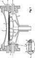
Wie aus
Der Abstand Δ zwischen dem Vorheizring
Um dem „autodoping”-Effekt entgegen zu wirken, hat der Spalt D zwischen dem Vorheizring
Der Abstand d zwischen einer äußeren seitlichen Begrenzung des Vorheizrings
Beispiel und Vergleichsbeispiel:Example and Comparative Example
Die vorteilhafte Wirkung, der Erfindung zeigt sich, wenn Eigenschaften wie der radiale Verlauf des spezifischen Widerstands der abgeschiedenen Schicht oder die Anzahl auf der abgeschiedenen Schicht nachgewiesenen Partikel bei Halbleiterscheiben aus Silizium, die mit einer epitaktisch abgeschiedenen Schicht aus Silizium versehen sind, verglichen werden.The advantageous effect of the invention is exhibited when properties such as the radial profile of the resistivity of the deposited layer or the number of particles detected on the deposited layer are compared with silicon wafers provided with an epitaxially deposited layer of silicon.
Claims (7)
Translated fromGermanPriority Applications (8)
| Application Number | Priority Date | Filing Date | Title |
|---|---|---|---|
| DE102011007632ADE102011007632B3 (en) | 2011-04-18 | 2011-04-18 | Device useful for depositing material layer derived from process gas on substrate disc, comprises reactor chamber, which is bound by upper cover, lower cover and side wall, susceptor, preheat ring, chuck, and spacer |
| US13/407,832US10240235B2 (en) | 2011-04-18 | 2012-02-29 | Method and apparatus for depositing a material layer originating from process gas on a substrate wafer |
| TW101111830ATWI467048B (en) | 2011-04-18 | 2012-04-03 | Method and apparatus for depositing a material layer originating from process gas on a substrate wafer |
| JP2012089225AJP5748699B2 (en) | 2011-04-18 | 2012-04-10 | Apparatus and method for depositing a layer of material |
| SG2012026605ASG185214A1 (en) | 2011-04-18 | 2012-04-12 | Method and apparatus for depositing a material layer originating from process gas on a substrate wafer |
| SG10201406621WASG10201406621WA (en) | 2011-04-18 | 2012-04-12 | Method and apparatus for depositing a material layer originating from process gas on a substrate wafer |
| KR1020120038146AKR101461272B1 (en) | 2011-04-18 | 2012-04-12 | Method and apparatus for depositing a material layer originating from process gas on a substrate wafer |
| CN201210109937.3ACN102751181B (en) | 2011-04-18 | 2012-04-13 | Method and apparatus for depositing a material layer originating from process gas on a substrate wafer |
Applications Claiming Priority (1)
| Application Number | Priority Date | Filing Date | Title |
|---|---|---|---|
| DE102011007632ADE102011007632B3 (en) | 2011-04-18 | 2011-04-18 | Device useful for depositing material layer derived from process gas on substrate disc, comprises reactor chamber, which is bound by upper cover, lower cover and side wall, susceptor, preheat ring, chuck, and spacer |
Publications (1)
| Publication Number | Publication Date |
|---|---|
| DE102011007632B3true DE102011007632B3 (en) | 2012-02-16 |
Family
ID=45528629
Family Applications (1)
| Application Number | Title | Priority Date | Filing Date |
|---|---|---|---|
| DE102011007632AExpired - Fee RelatedDE102011007632B3 (en) | 2011-04-18 | 2011-04-18 | Device useful for depositing material layer derived from process gas on substrate disc, comprises reactor chamber, which is bound by upper cover, lower cover and side wall, susceptor, preheat ring, chuck, and spacer |
Country Status (7)
| Country | Link |
|---|---|
| US (1) | US10240235B2 (en) |
| JP (1) | JP5748699B2 (en) |
| KR (1) | KR101461272B1 (en) |
| CN (1) | CN102751181B (en) |
| DE (1) | DE102011007632B3 (en) |
| SG (2) | SG185214A1 (en) |
| TW (1) | TWI467048B (en) |
Cited By (4)
| Publication number | Priority date | Publication date | Assignee | Title |
|---|---|---|---|---|
| WO2018087120A1 (en)* | 2016-11-10 | 2018-05-17 | Aixtron Se | Device and method to control the uniformity of a gas flow in a cvd or an ald reactor or of a layer grown therein |
| CN112185881A (en)* | 2019-07-05 | 2021-01-05 | 东京毅力科创株式会社 | Mounting table, substrate processing apparatus, and mounting table assembling method |
| EP3978647A1 (en)* | 2020-09-30 | 2022-04-06 | Siltronic AG | Method and device for depositing an epitaxial layer on a substrate wafer of semiconductor material |
| EP4219804A4 (en)* | 2020-09-28 | 2024-11-27 | Epicrew Corporation | VAPOR DEPOSITION APPARATUS AND METHOD FOR PRODUCING AN EPITATICAL WAFER |
Families Citing this family (246)
| Publication number | Priority date | Publication date | Assignee | Title |
|---|---|---|---|---|
| US20130023129A1 (en) | 2011-07-20 | 2013-01-24 | Asm America, Inc. | Pressure transmitter for a semiconductor processing environment |
| US20160376700A1 (en) | 2013-02-01 | 2016-12-29 | Asm Ip Holding B.V. | System for treatment of deposition reactor |
| TWI648427B (en)* | 2013-07-17 | 2019-01-21 | 應用材料股份有限公司 | Structure for improved gas activation for cross-flow type thermal cvd chamber |
| US10047457B2 (en) | 2013-09-16 | 2018-08-14 | Applied Materials, Inc. | EPI pre-heat ring |
| DE102013218883B4 (en) | 2013-09-19 | 2018-12-06 | Siltronic Ag | Apparatus and method for depositing semiconductor material from a gaseous phase onto a substrate wafer |
| KR101539298B1 (en)* | 2013-11-25 | 2015-07-29 | 주식회사 엘지실트론 | Apparatus for Growing Epitaxial Wafer |
| WO2015084487A1 (en)* | 2013-12-06 | 2015-06-11 | Applied Materials, Inc. | Apparatus for self centering preheat member |
| US10941490B2 (en) | 2014-10-07 | 2021-03-09 | Asm Ip Holding B.V. | Multiple temperature range susceptor, assembly, reactor and system including the susceptor, and methods of using the same |
| JP6341083B2 (en)* | 2014-12-25 | 2018-06-13 | 株式会社Sumco | Epitaxial silicon wafer manufacturing method |
| US10276355B2 (en) | 2015-03-12 | 2019-04-30 | Asm Ip Holding B.V. | Multi-zone reactor, system including the reactor, and method of using the same |
| WO2017059114A1 (en)* | 2015-10-01 | 2017-04-06 | Sunedison Semiconductor Limited | Cvd apparatus |
| US11139308B2 (en) | 2015-12-29 | 2021-10-05 | Asm Ip Holding B.V. | Atomic layer deposition of III-V compounds to form V-NAND devices |
| US10529554B2 (en) | 2016-02-19 | 2020-01-07 | Asm Ip Holding B.V. | Method for forming silicon nitride film selectively on sidewalls or flat surfaces of trenches |
| US10343920B2 (en) | 2016-03-18 | 2019-07-09 | Asm Ip Holding B.V. | Aligned carbon nanotubes |
| US11453943B2 (en) | 2016-05-25 | 2022-09-27 | Asm Ip Holding B.V. | Method for forming carbon-containing silicon/metal oxide or nitride film by ALD using silicon precursor and hydrocarbon precursor |
| US9859151B1 (en) | 2016-07-08 | 2018-01-02 | Asm Ip Holding B.V. | Selective film deposition method to form air gaps |
| US10612137B2 (en) | 2016-07-08 | 2020-04-07 | Asm Ip Holdings B.V. | Organic reactants for atomic layer deposition |
| US9887082B1 (en) | 2016-07-28 | 2018-02-06 | Asm Ip Holding B.V. | Method and apparatus for filling a gap |
| US9812320B1 (en) | 2016-07-28 | 2017-11-07 | Asm Ip Holding B.V. | Method and apparatus for filling a gap |
| US11532757B2 (en) | 2016-10-27 | 2022-12-20 | Asm Ip Holding B.V. | Deposition of charge trapping layers |
| US10714350B2 (en) | 2016-11-01 | 2020-07-14 | ASM IP Holdings, B.V. | Methods for forming a transition metal niobium nitride film on a substrate by atomic layer deposition and related semiconductor device structures |
| KR102546317B1 (en) | 2016-11-15 | 2023-06-21 | 에이에스엠 아이피 홀딩 비.브이. | Gas supply unit and substrate processing apparatus including the same |
| US11447861B2 (en) | 2016-12-15 | 2022-09-20 | Asm Ip Holding B.V. | Sequential infiltration synthesis apparatus and a method of forming a patterned structure |
| US11581186B2 (en) | 2016-12-15 | 2023-02-14 | Asm Ip Holding B.V. | Sequential infiltration synthesis apparatus |
| US11390950B2 (en) | 2017-01-10 | 2022-07-19 | Asm Ip Holding B.V. | Reactor system and method to reduce residue buildup during a film deposition process |
| US10468261B2 (en) | 2017-02-15 | 2019-11-05 | Asm Ip Holding B.V. | Methods for forming a metallic film on a substrate by cyclical deposition and related semiconductor device structures |
| US10770286B2 (en) | 2017-05-08 | 2020-09-08 | Asm Ip Holdings B.V. | Methods for selectively forming a silicon nitride film on a substrate and related semiconductor device structures |
| US12040200B2 (en) | 2017-06-20 | 2024-07-16 | Asm Ip Holding B.V. | Semiconductor processing apparatus and methods for calibrating a semiconductor processing apparatus |
| US11306395B2 (en) | 2017-06-28 | 2022-04-19 | Asm Ip Holding B.V. | Methods for depositing a transition metal nitride film on a substrate by atomic layer deposition and related deposition apparatus |
| KR20190009245A (en) | 2017-07-18 | 2019-01-28 | 에이에스엠 아이피 홀딩 비.브이. | Methods for forming a semiconductor device structure and related semiconductor device structures |
| US11374112B2 (en) | 2017-07-19 | 2022-06-28 | Asm Ip Holding B.V. | Method for depositing a group IV semiconductor and related semiconductor device structures |
| US10590535B2 (en) | 2017-07-26 | 2020-03-17 | Asm Ip Holdings B.V. | Chemical treatment, deposition and/or infiltration apparatus and method for using the same |
| TWI815813B (en) | 2017-08-04 | 2023-09-21 | 荷蘭商Asm智慧財產控股公司 | Showerhead assembly for distributing a gas within a reaction chamber |
| US10692741B2 (en) | 2017-08-08 | 2020-06-23 | Asm Ip Holdings B.V. | Radiation shield |
| US10770336B2 (en) | 2017-08-08 | 2020-09-08 | Asm Ip Holding B.V. | Substrate lift mechanism and reactor including same |
| US11769682B2 (en) | 2017-08-09 | 2023-09-26 | Asm Ip Holding B.V. | Storage apparatus for storing cassettes for substrates and processing apparatus equipped therewith |
| US11830730B2 (en) | 2017-08-29 | 2023-11-28 | Asm Ip Holding B.V. | Layer forming method and apparatus |
| US11295980B2 (en) | 2017-08-30 | 2022-04-05 | Asm Ip Holding B.V. | Methods for depositing a molybdenum metal film over a dielectric surface of a substrate by a cyclical deposition process and related semiconductor device structures |
| US10658205B2 (en) | 2017-09-28 | 2020-05-19 | Asm Ip Holdings B.V. | Chemical dispensing apparatus and methods for dispensing a chemical to a reaction chamber |
| US10403504B2 (en) | 2017-10-05 | 2019-09-03 | Asm Ip Holding B.V. | Method for selectively depositing a metallic film on a substrate |
| US10923344B2 (en) | 2017-10-30 | 2021-02-16 | Asm Ip Holding B.V. | Methods for forming a semiconductor structure and related semiconductor structures |
| CN111344522B (en) | 2017-11-27 | 2022-04-12 | 阿斯莫Ip控股公司 | Including clean mini-environment device |
| WO2019103613A1 (en) | 2017-11-27 | 2019-05-31 | Asm Ip Holding B.V. | A storage device for storing wafer cassettes for use with a batch furnace |
| US10872771B2 (en) | 2018-01-16 | 2020-12-22 | Asm Ip Holding B. V. | Method for depositing a material film on a substrate within a reaction chamber by a cyclical deposition process and related device structures |
| TWI799494B (en) | 2018-01-19 | 2023-04-21 | 荷蘭商Asm 智慧財產控股公司 | Deposition method |
| KR102695659B1 (en) | 2018-01-19 | 2024-08-14 | 에이에스엠 아이피 홀딩 비.브이. | Method for depositing a gap filling layer by plasma assisted deposition |
| US11081345B2 (en) | 2018-02-06 | 2021-08-03 | Asm Ip Holding B.V. | Method of post-deposition treatment for silicon oxide film |
| WO2019158960A1 (en) | 2018-02-14 | 2019-08-22 | Asm Ip Holding B.V. | A method for depositing a ruthenium-containing film on a substrate by a cyclical deposition process |
| US10896820B2 (en) | 2018-02-14 | 2021-01-19 | Asm Ip Holding B.V. | Method for depositing a ruthenium-containing film on a substrate by a cyclical deposition process |
| US10731249B2 (en) | 2018-02-15 | 2020-08-04 | Asm Ip Holding B.V. | Method of forming a transition metal containing film on a substrate by a cyclical deposition process, a method for supplying a transition metal halide compound to a reaction chamber, and related vapor deposition apparatus |
| KR102636427B1 (en) | 2018-02-20 | 2024-02-13 | 에이에스엠 아이피 홀딩 비.브이. | Substrate processing method and apparatus |
| US10975470B2 (en) | 2018-02-23 | 2021-04-13 | Asm Ip Holding B.V. | Apparatus for detecting or monitoring for a chemical precursor in a high temperature environment |
| US11473195B2 (en) | 2018-03-01 | 2022-10-18 | Asm Ip Holding B.V. | Semiconductor processing apparatus and a method for processing a substrate |
| KR102646467B1 (en) | 2018-03-27 | 2024-03-11 | 에이에스엠 아이피 홀딩 비.브이. | Method of forming an electrode on a substrate and a semiconductor device structure including an electrode |
| KR102600229B1 (en) | 2018-04-09 | 2023-11-10 | 에이에스엠 아이피 홀딩 비.브이. | Substrate supporting device, substrate processing apparatus including the same and substrate processing method |
| US12025484B2 (en) | 2018-05-08 | 2024-07-02 | Asm Ip Holding B.V. | Thin film forming method |
| US12272527B2 (en) | 2018-05-09 | 2025-04-08 | Asm Ip Holding B.V. | Apparatus for use with hydrogen radicals and method of using same |
| KR102596988B1 (en) | 2018-05-28 | 2023-10-31 | 에이에스엠 아이피 홀딩 비.브이. | Method of processing a substrate and a device manufactured by the same |
| US11718913B2 (en) | 2018-06-04 | 2023-08-08 | Asm Ip Holding B.V. | Gas distribution system and reactor system including same |
| US10797133B2 (en) | 2018-06-21 | 2020-10-06 | Asm Ip Holding B.V. | Method for depositing a phosphorus doped silicon arsenide film and related semiconductor device structures |
| KR102568797B1 (en) | 2018-06-21 | 2023-08-21 | 에이에스엠 아이피 홀딩 비.브이. | Substrate processing system |
| JP6998839B2 (en)* | 2018-06-25 | 2022-01-18 | グローバルウェーハズ・ジャパン株式会社 | Manufacturing method of epitaxial silicon wafer |
| TWI873894B (en) | 2018-06-27 | 2025-02-21 | 荷蘭商Asm Ip私人控股有限公司 | Cyclic deposition methods for forming metal-containing material and films and structures including the metal-containing material |
| KR102854019B1 (en) | 2018-06-27 | 2025-09-02 | 에이에스엠 아이피 홀딩 비.브이. | Periodic deposition method for forming a metal-containing material and films and structures comprising the metal-containing material |
| US10388513B1 (en) | 2018-07-03 | 2019-08-20 | Asm Ip Holding B.V. | Method for depositing silicon-free carbon-containing film as gap-fill layer by pulse plasma-assisted deposition |
| US10755922B2 (en) | 2018-07-03 | 2020-08-25 | Asm Ip Holding B.V. | Method for depositing silicon-free carbon-containing film as gap-fill layer by pulse plasma-assisted deposition |
| US11430674B2 (en) | 2018-08-22 | 2022-08-30 | Asm Ip Holding B.V. | Sensor array, apparatus for dispensing a vapor phase reactant to a reaction chamber and related methods |
| KR102707956B1 (en) | 2018-09-11 | 2024-09-19 | 에이에스엠 아이피 홀딩 비.브이. | Method for deposition of a thin film |
| US11024523B2 (en) | 2018-09-11 | 2021-06-01 | Asm Ip Holding B.V. | Substrate processing apparatus and method |
| CN110970344B (en) | 2018-10-01 | 2024-10-25 | Asmip控股有限公司 | Substrate holding apparatus, system comprising the same and method of using the same |
| KR102592699B1 (en) | 2018-10-08 | 2023-10-23 | 에이에스엠 아이피 홀딩 비.브이. | Substrate support unit and apparatuses for depositing thin film and processing the substrate including the same |
| KR102546322B1 (en) | 2018-10-19 | 2023-06-21 | 에이에스엠 아이피 홀딩 비.브이. | Substrate processing apparatus and substrate processing method |
| US12378665B2 (en) | 2018-10-26 | 2025-08-05 | Asm Ip Holding B.V. | High temperature coatings for a preclean and etch apparatus and related methods |
| US11087997B2 (en) | 2018-10-31 | 2021-08-10 | Asm Ip Holding B.V. | Substrate processing apparatus for processing substrates |
| KR102748291B1 (en) | 2018-11-02 | 2024-12-31 | 에이에스엠 아이피 홀딩 비.브이. | Substrate support unit and substrate processing apparatus including the same |
| US11572620B2 (en) | 2018-11-06 | 2023-02-07 | Asm Ip Holding B.V. | Methods for selectively depositing an amorphous silicon film on a substrate |
| US10818758B2 (en) | 2018-11-16 | 2020-10-27 | Asm Ip Holding B.V. | Methods for forming a metal silicate film on a substrate in a reaction chamber and related semiconductor device structures |
| US12040199B2 (en) | 2018-11-28 | 2024-07-16 | Asm Ip Holding B.V. | Substrate processing apparatus for processing substrates |
| KR102636428B1 (en) | 2018-12-04 | 2024-02-13 | 에이에스엠 아이피 홀딩 비.브이. | A method for cleaning a substrate processing apparatus |
| US11158513B2 (en) | 2018-12-13 | 2021-10-26 | Asm Ip Holding B.V. | Methods for forming a rhenium-containing film on a substrate by a cyclical deposition process and related semiconductor device structures |
| TWI874340B (en) | 2018-12-14 | 2025-03-01 | 荷蘭商Asm Ip私人控股有限公司 | Method of forming device structure, structure formed by the method and system for performing the method |
| TWI866480B (en) | 2019-01-17 | 2024-12-11 | 荷蘭商Asm Ip 私人控股有限公司 | Methods of forming a transition metal containing film on a substrate by a cyclical deposition process |
| TWI838458B (en) | 2019-02-20 | 2024-04-11 | 荷蘭商Asm Ip私人控股有限公司 | Apparatus and methods for plug fill deposition in 3-d nand applications |
| TWI845607B (en) | 2019-02-20 | 2024-06-21 | 荷蘭商Asm Ip私人控股有限公司 | Cyclical deposition method and apparatus for filling a recess formed within a substrate surface |
| TWI873122B (en) | 2019-02-20 | 2025-02-21 | 荷蘭商Asm Ip私人控股有限公司 | Method of filling a recess formed within a surface of a substrate, semiconductor structure formed according to the method, and semiconductor processing apparatus |
| TWI842826B (en) | 2019-02-22 | 2024-05-21 | 荷蘭商Asm Ip私人控股有限公司 | Substrate processing apparatus and method for processing substrate |
| US11742198B2 (en) | 2019-03-08 | 2023-08-29 | Asm Ip Holding B.V. | Structure including SiOCN layer and method of forming same |
| KR102858005B1 (en) | 2019-03-08 | 2025-09-09 | 에이에스엠 아이피 홀딩 비.브이. | Method for Selective Deposition of Silicon Nitride Layer and Structure Including Selectively-Deposited Silicon Nitride Layer |
| JP2020167398A (en) | 2019-03-28 | 2020-10-08 | エーエスエム・アイピー・ホールディング・ベー・フェー | Door openers and substrate processing equipment provided with door openers |
| KR102809999B1 (en) | 2019-04-01 | 2025-05-19 | 에이에스엠 아이피 홀딩 비.브이. | Method of manufacturing semiconductor device |
| KR20200123380A (en) | 2019-04-19 | 2020-10-29 | 에이에스엠 아이피 홀딩 비.브이. | Layer forming method and apparatus |
| KR20200125453A (en) | 2019-04-24 | 2020-11-04 | 에이에스엠 아이피 홀딩 비.브이. | Gas-phase reactor system and method of using same |
| KR20200130121A (en) | 2019-05-07 | 2020-11-18 | 에이에스엠 아이피 홀딩 비.브이. | Chemical source vessel with dip tube |
| KR20200130652A (en) | 2019-05-10 | 2020-11-19 | 에이에스엠 아이피 홀딩 비.브이. | Method of depositing material onto a surface and structure formed according to the method |
| JP7612342B2 (en) | 2019-05-16 | 2025-01-14 | エーエスエム・アイピー・ホールディング・ベー・フェー | Wafer boat handling apparatus, vertical batch furnace and method |
| JP7598201B2 (en) | 2019-05-16 | 2024-12-11 | エーエスエム・アイピー・ホールディング・ベー・フェー | Wafer boat handling apparatus, vertical batch furnace and method |
| USD947913S1 (en) | 2019-05-17 | 2022-04-05 | Asm Ip Holding B.V. | Susceptor shaft |
| USD975665S1 (en) | 2019-05-17 | 2023-01-17 | Asm Ip Holding B.V. | Susceptor shaft |
| JP2020191346A (en)* | 2019-05-21 | 2020-11-26 | クアーズテック株式会社 | Susceptor and epitaxial growth device |
| KR20200141002A (en) | 2019-06-06 | 2020-12-17 | 에이에스엠 아이피 홀딩 비.브이. | Method of using a gas-phase reactor system including analyzing exhausted gas |
| KR20200141931A (en) | 2019-06-10 | 2020-12-21 | 에이에스엠 아이피 홀딩 비.브이. | Method for cleaning quartz epitaxial chambers |
| KR20200143254A (en) | 2019-06-11 | 2020-12-23 | 에이에스엠 아이피 홀딩 비.브이. | Method of forming an electronic structure using an reforming gas, system for performing the method, and structure formed using the method |
| JP7159986B2 (en)* | 2019-06-27 | 2022-10-25 | 株式会社Sumco | Epitaxial growth apparatus and epitaxial wafer manufacturing method |
| KR20210005515A (en) | 2019-07-03 | 2021-01-14 | 에이에스엠 아이피 홀딩 비.브이. | Temperature control assembly for substrate processing apparatus and method of using same |
| JP7499079B2 (en) | 2019-07-09 | 2024-06-13 | エーエスエム・アイピー・ホールディング・ベー・フェー | Plasma device using coaxial waveguide and substrate processing method |
| CN112216646A (en) | 2019-07-10 | 2021-01-12 | Asm Ip私人控股有限公司 | Substrate supporting assembly and substrate processing device comprising same |
| KR20210010307A (en) | 2019-07-16 | 2021-01-27 | 에이에스엠 아이피 홀딩 비.브이. | Substrate processing apparatus |
| KR20210010816A (en) | 2019-07-17 | 2021-01-28 | 에이에스엠 아이피 홀딩 비.브이. | Radical assist ignition plasma system and method |
| KR102860110B1 (en) | 2019-07-17 | 2025-09-16 | 에이에스엠 아이피 홀딩 비.브이. | Methods of forming silicon germanium structures |
| US11643724B2 (en) | 2019-07-18 | 2023-05-09 | Asm Ip Holding B.V. | Method of forming structures using a neutral beam |
| KR20210010817A (en) | 2019-07-19 | 2021-01-28 | 에이에스엠 아이피 홀딩 비.브이. | Method of Forming Topology-Controlled Amorphous Carbon Polymer Film |
| TWI851767B (en) | 2019-07-29 | 2024-08-11 | 荷蘭商Asm Ip私人控股有限公司 | Methods for selective deposition utilizing n-type dopants and/or alternative dopants to achieve high dopant incorporation |
| CN112309899A (en) | 2019-07-30 | 2021-02-02 | Asm Ip私人控股有限公司 | Substrate processing apparatus |
| CN112309900A (en) | 2019-07-30 | 2021-02-02 | Asm Ip私人控股有限公司 | Substrate processing apparatus |
| US12169361B2 (en) | 2019-07-30 | 2024-12-17 | Asm Ip Holding B.V. | Substrate processing apparatus and method |
| US11587814B2 (en) | 2019-07-31 | 2023-02-21 | Asm Ip Holding B.V. | Vertical batch furnace assembly |
| US11227782B2 (en) | 2019-07-31 | 2022-01-18 | Asm Ip Holding B.V. | Vertical batch furnace assembly |
| US11587815B2 (en) | 2019-07-31 | 2023-02-21 | Asm Ip Holding B.V. | Vertical batch furnace assembly |
| CN112323048B (en) | 2019-08-05 | 2024-02-09 | Asm Ip私人控股有限公司 | Liquid level sensor for chemical source container |
| CN112342526A (en) | 2019-08-09 | 2021-02-09 | Asm Ip私人控股有限公司 | Heater assembly including cooling device and method of using same |
| USD965044S1 (en) | 2019-08-19 | 2022-09-27 | Asm Ip Holding B.V. | Susceptor shaft |
| USD965524S1 (en) | 2019-08-19 | 2022-10-04 | Asm Ip Holding B.V. | Susceptor support |
| JP2021031769A (en) | 2019-08-21 | 2021-03-01 | エーエスエム アイピー ホールディング ビー.ブイ. | Production apparatus of mixed gas of film deposition raw material and film deposition apparatus |
| KR20210024423A (en) | 2019-08-22 | 2021-03-05 | 에이에스엠 아이피 홀딩 비.브이. | Method for forming a structure with a hole |
| USD979506S1 (en) | 2019-08-22 | 2023-02-28 | Asm Ip Holding B.V. | Insulator |
| US11286558B2 (en) | 2019-08-23 | 2022-03-29 | Asm Ip Holding B.V. | Methods for depositing a molybdenum nitride film on a surface of a substrate by a cyclical deposition process and related semiconductor device structures including a molybdenum nitride film |
| KR20210024420A (en) | 2019-08-23 | 2021-03-05 | 에이에스엠 아이피 홀딩 비.브이. | Method for depositing silicon oxide film having improved quality by peald using bis(diethylamino)silane |
| KR102806450B1 (en) | 2019-09-04 | 2025-05-12 | 에이에스엠 아이피 홀딩 비.브이. | Methods for selective deposition using a sacrificial capping layer |
| KR102733104B1 (en) | 2019-09-05 | 2024-11-22 | 에이에스엠 아이피 홀딩 비.브이. | Substrate processing apparatus |
| US11562901B2 (en) | 2019-09-25 | 2023-01-24 | Asm Ip Holding B.V. | Substrate processing method |
| CN112593212B (en) | 2019-10-02 | 2023-12-22 | Asm Ip私人控股有限公司 | Method for forming topologically selective silicon oxide film by cyclic plasma enhanced deposition process |
| TW202128273A (en) | 2019-10-08 | 2021-08-01 | 荷蘭商Asm Ip私人控股有限公司 | Gas injection system, reactor system, and method of depositing material on surface of substratewithin reaction chamber |
| TWI846953B (en) | 2019-10-08 | 2024-07-01 | 荷蘭商Asm Ip私人控股有限公司 | Substrate processing device |
| KR20210042810A (en) | 2019-10-08 | 2021-04-20 | 에이에스엠 아이피 홀딩 비.브이. | Reactor system including a gas distribution assembly for use with activated species and method of using same |
| TWI846966B (en) | 2019-10-10 | 2024-07-01 | 荷蘭商Asm Ip私人控股有限公司 | Method of forming a photoresist underlayer and structure including same |
| US12009241B2 (en) | 2019-10-14 | 2024-06-11 | Asm Ip Holding B.V. | Vertical batch furnace assembly with detector to detect cassette |
| TWI834919B (en) | 2019-10-16 | 2024-03-11 | 荷蘭商Asm Ip私人控股有限公司 | Method of topology-selective film formation of silicon oxide |
| US11637014B2 (en) | 2019-10-17 | 2023-04-25 | Asm Ip Holding B.V. | Methods for selective deposition of doped semiconductor material |
| KR102845724B1 (en) | 2019-10-21 | 2025-08-13 | 에이에스엠 아이피 홀딩 비.브이. | Apparatus and methods for selectively etching films |
| KR20210050453A (en) | 2019-10-25 | 2021-05-07 | 에이에스엠 아이피 홀딩 비.브이. | Methods for filling a gap feature on a substrate surface and related semiconductor structures |
| US11646205B2 (en) | 2019-10-29 | 2023-05-09 | Asm Ip Holding B.V. | Methods of selectively forming n-type doped material on a surface, systems for selectively forming n-type doped material, and structures formed using same |
| KR20210054983A (en) | 2019-11-05 | 2021-05-14 | 에이에스엠 아이피 홀딩 비.브이. | Structures with doped semiconductor layers and methods and systems for forming same |
| US11501968B2 (en) | 2019-11-15 | 2022-11-15 | Asm Ip Holding B.V. | Method for providing a semiconductor device with silicon filled gaps |
| KR102861314B1 (en) | 2019-11-20 | 2025-09-17 | 에이에스엠 아이피 홀딩 비.브이. | Method of depositing carbon-containing material on a surface of a substrate, structure formed using the method, and system for forming the structure |
| CN112951697B (en) | 2019-11-26 | 2025-07-29 | Asmip私人控股有限公司 | Substrate processing apparatus |
| US11450529B2 (en) | 2019-11-26 | 2022-09-20 | Asm Ip Holding B.V. | Methods for selectively forming a target film on a substrate comprising a first dielectric surface and a second metallic surface |
| CN120432376A (en) | 2019-11-29 | 2025-08-05 | Asm Ip私人控股有限公司 | Substrate processing apparatus |
| CN112885692B (en) | 2019-11-29 | 2025-08-15 | Asmip私人控股有限公司 | Substrate processing apparatus |
| JP7527928B2 (en) | 2019-12-02 | 2024-08-05 | エーエスエム・アイピー・ホールディング・ベー・フェー | Substrate processing apparatus and substrate processing method |
| KR20210070898A (en) | 2019-12-04 | 2021-06-15 | 에이에스엠 아이피 홀딩 비.브이. | Substrate processing apparatus |
| KR20210078405A (en) | 2019-12-17 | 2021-06-28 | 에이에스엠 아이피 홀딩 비.브이. | Method of forming vanadium nitride layer and structure including the vanadium nitride layer |
| KR20210080214A (en) | 2019-12-19 | 2021-06-30 | 에이에스엠 아이피 홀딩 비.브이. | Methods for filling a gap feature on a substrate and related semiconductor structures |
| JP7636892B2 (en) | 2020-01-06 | 2025-02-27 | エーエスエム・アイピー・ホールディング・ベー・フェー | Channeled Lift Pins |
| JP7730637B2 (en) | 2020-01-06 | 2025-08-28 | エーエスエム・アイピー・ホールディング・ベー・フェー | Gas delivery assembly, components thereof, and reactor system including same |
| US11993847B2 (en) | 2020-01-08 | 2024-05-28 | Asm Ip Holding B.V. | Injector |
| KR20210093163A (en) | 2020-01-16 | 2021-07-27 | 에이에스엠 아이피 홀딩 비.브이. | Method of forming high aspect ratio features |
| KR102675856B1 (en) | 2020-01-20 | 2024-06-17 | 에이에스엠 아이피 홀딩 비.브이. | Method of forming thin film and method of modifying surface of thin film |
| TWI889744B (en) | 2020-01-29 | 2025-07-11 | 荷蘭商Asm Ip私人控股有限公司 | Contaminant trap system, and baffle plate stack |
| TW202513845A (en) | 2020-02-03 | 2025-04-01 | 荷蘭商Asm Ip私人控股有限公司 | Semiconductor structures and methods for forming the same |
| KR20210100010A (en) | 2020-02-04 | 2021-08-13 | 에이에스엠 아이피 홀딩 비.브이. | Method and apparatus for transmittance measurements of large articles |
| US11776846B2 (en) | 2020-02-07 | 2023-10-03 | Asm Ip Holding B.V. | Methods for depositing gap filling fluids and related systems and devices |
| KR20210103956A (en) | 2020-02-13 | 2021-08-24 | 에이에스엠 아이피 홀딩 비.브이. | Substrate processing apparatus including light receiving device and calibration method of light receiving device |
| TW202146691A (en) | 2020-02-13 | 2021-12-16 | 荷蘭商Asm Ip私人控股有限公司 | Gas distribution assembly, shower plate assembly, and method of adjusting conductance of gas to reaction chamber |
| TWI855223B (en) | 2020-02-17 | 2024-09-11 | 荷蘭商Asm Ip私人控股有限公司 | Method for growing phosphorous-doped silicon layer |
| CN113410160A (en) | 2020-02-28 | 2021-09-17 | Asm Ip私人控股有限公司 | System specially used for cleaning parts |
| KR20210113043A (en) | 2020-03-04 | 2021-09-15 | 에이에스엠 아이피 홀딩 비.브이. | Alignment fixture for a reactor system |
| KR20210116240A (en) | 2020-03-11 | 2021-09-27 | 에이에스엠 아이피 홀딩 비.브이. | Substrate handling device with adjustable joints |
| US11876356B2 (en) | 2020-03-11 | 2024-01-16 | Asm Ip Holding B.V. | Lockout tagout assembly and system and method of using same |
| KR102775390B1 (en) | 2020-03-12 | 2025-02-28 | 에이에스엠 아이피 홀딩 비.브이. | Method for Fabricating Layer Structure Having Target Topological Profile |
| US12173404B2 (en) | 2020-03-17 | 2024-12-24 | Asm Ip Holding B.V. | Method of depositing epitaxial material, structure formed using the method, and system for performing the method |
| KR102755229B1 (en) | 2020-04-02 | 2025-01-14 | 에이에스엠 아이피 홀딩 비.브이. | Thin film forming method |
| TWI887376B (en) | 2020-04-03 | 2025-06-21 | 荷蘭商Asm Ip私人控股有限公司 | Method for manufacturing semiconductor device |
| TWI888525B (en) | 2020-04-08 | 2025-07-01 | 荷蘭商Asm Ip私人控股有限公司 | Apparatus and methods for selectively etching silcon oxide films |
| KR20210127620A (en) | 2020-04-13 | 2021-10-22 | 에이에스엠 아이피 홀딩 비.브이. | method of forming a nitrogen-containing carbon film and system for performing the method |
| US11821078B2 (en) | 2020-04-15 | 2023-11-21 | Asm Ip Holding B.V. | Method for forming precoat film and method for forming silicon-containing film |
| KR20210128343A (en) | 2020-04-15 | 2021-10-26 | 에이에스엠 아이피 홀딩 비.브이. | Method of forming chromium nitride layer and structure including the chromium nitride layer |
| US11996289B2 (en) | 2020-04-16 | 2024-05-28 | Asm Ip Holding B.V. | Methods of forming structures including silicon germanium and silicon layers, devices formed using the methods, and systems for performing the methods |
| KR20210130646A (en) | 2020-04-21 | 2021-11-01 | 에이에스엠 아이피 홀딩 비.브이. | Method for processing a substrate |
| KR20210132612A (en) | 2020-04-24 | 2021-11-04 | 에이에스엠 아이피 홀딩 비.브이. | Methods and apparatus for stabilizing vanadium compounds |
| TW202208671A (en) | 2020-04-24 | 2022-03-01 | 荷蘭商Asm Ip私人控股有限公司 | Methods of forming structures including vanadium boride and vanadium phosphide layers |
| KR102866804B1 (en) | 2020-04-24 | 2025-09-30 | 에이에스엠 아이피 홀딩 비.브이. | Vertical batch furnace assembly comprising a cooling gas supply |
| KR20210132600A (en) | 2020-04-24 | 2021-11-04 | 에이에스엠 아이피 홀딩 비.브이. | Methods and systems for depositing a layer comprising vanadium, nitrogen, and a further element |
| CN113555279A (en) | 2020-04-24 | 2021-10-26 | Asm Ip私人控股有限公司 | Methods of forming vanadium nitride-containing layers and structures comprising the same |
| EP3905311A1 (en)* | 2020-04-27 | 2021-11-03 | Siltronic AG | Method and device for depositing an epitaxial layer on a substrate wafer of semiconductor material |
| KR102783898B1 (en) | 2020-04-29 | 2025-03-18 | 에이에스엠 아이피 홀딩 비.브이. | Solid source precursor vessel |
| KR20210134869A (en) | 2020-05-01 | 2021-11-11 | 에이에스엠 아이피 홀딩 비.브이. | Fast FOUP swapping with a FOUP handler |
| JP7726664B2 (en) | 2020-05-04 | 2025-08-20 | エーエスエム・アイピー・ホールディング・ベー・フェー | Substrate processing system for processing a substrate |
| KR20210137395A (en) | 2020-05-07 | 2021-11-17 | 에이에스엠 아이피 홀딩 비.브이. | Apparatus and methods for performing an in-situ etch of reaction chambers with fluorine-based radicals |
| KR102788543B1 (en) | 2020-05-13 | 2025-03-27 | 에이에스엠 아이피 홀딩 비.브이. | Laser alignment fixture for a reactor system |
| TW202146699A (en) | 2020-05-15 | 2021-12-16 | 荷蘭商Asm Ip私人控股有限公司 | Method of forming a silicon germanium layer, semiconductor structure, semiconductor device, method of forming a deposition layer, and deposition system |
| KR20210143653A (en) | 2020-05-19 | 2021-11-29 | 에이에스엠 아이피 홀딩 비.브이. | Substrate processing apparatus |
| KR102795476B1 (en) | 2020-05-21 | 2025-04-11 | 에이에스엠 아이피 홀딩 비.브이. | Structures including multiple carbon layers and methods of forming and using same |
| KR20210145079A (en) | 2020-05-21 | 2021-12-01 | 에이에스엠 아이피 홀딩 비.브이. | Flange and apparatus for processing substrates |
| TWI873343B (en) | 2020-05-22 | 2025-02-21 | 荷蘭商Asm Ip私人控股有限公司 | Reaction system for forming thin film on substrate |
| KR20210146802A (en) | 2020-05-26 | 2021-12-06 | 에이에스엠 아이피 홀딩 비.브이. | Method for depositing boron and gallium containing silicon germanium layers |
| TWI876048B (en) | 2020-05-29 | 2025-03-11 | 荷蘭商Asm Ip私人控股有限公司 | Substrate processing device |
| TW202212620A (en) | 2020-06-02 | 2022-04-01 | 荷蘭商Asm Ip私人控股有限公司 | Apparatus for processing substrate, method of forming film, and method of controlling apparatus for processing substrate |
| TW202208659A (en) | 2020-06-16 | 2022-03-01 | 荷蘭商Asm Ip私人控股有限公司 | Method for depositing boron containing silicon germanium layers |
| TW202218133A (en) | 2020-06-24 | 2022-05-01 | 荷蘭商Asm Ip私人控股有限公司 | Method for forming a layer provided with silicon |
| TWI873359B (en) | 2020-06-30 | 2025-02-21 | 荷蘭商Asm Ip私人控股有限公司 | Substrate processing method |
| TW202202649A (en) | 2020-07-08 | 2022-01-16 | 荷蘭商Asm Ip私人控股有限公司 | Substrate processing method |
| KR20220010438A (en) | 2020-07-17 | 2022-01-25 | 에이에스엠 아이피 홀딩 비.브이. | Structures and methods for use in photolithography |
| KR20220011092A (en) | 2020-07-20 | 2022-01-27 | 에이에스엠 아이피 홀딩 비.브이. | Method and system for forming structures including transition metal layers |
| TWI878570B (en) | 2020-07-20 | 2025-04-01 | 荷蘭商Asm Ip私人控股有限公司 | Method and system for depositing molybdenum layers |
| US12322591B2 (en) | 2020-07-27 | 2025-06-03 | Asm Ip Holding B.V. | Thin film deposition process |
| KR20220021863A (en) | 2020-08-14 | 2022-02-22 | 에이에스엠 아이피 홀딩 비.브이. | Method for processing a substrate |
| US12040177B2 (en) | 2020-08-18 | 2024-07-16 | Asm Ip Holding B.V. | Methods for forming a laminate film by cyclical plasma-enhanced deposition processes |
| TW202228863A (en) | 2020-08-25 | 2022-08-01 | 荷蘭商Asm Ip私人控股有限公司 | Method for cleaning a substrate, method for selectively depositing, and reaction system |
| US11725280B2 (en) | 2020-08-26 | 2023-08-15 | Asm Ip Holding B.V. | Method for forming metal silicon oxide and metal silicon oxynitride layers |
| TW202229601A (en) | 2020-08-27 | 2022-08-01 | 荷蘭商Asm Ip私人控股有限公司 | Method of forming patterned structures, method of manipulating mechanical property, device structure, and substrate processing system |
| CN112133669B (en)* | 2020-09-01 | 2024-03-26 | 北京北方华创微电子装备有限公司 | Semiconductor chamber and semiconductor device |
| USD990534S1 (en) | 2020-09-11 | 2023-06-27 | Asm Ip Holding B.V. | Weighted lift pin |
| KR20220036866A (en) | 2020-09-16 | 2022-03-23 | 에이에스엠 아이피 홀딩 비.브이. | Silicon oxide deposition method |
| USD1012873S1 (en) | 2020-09-24 | 2024-01-30 | Asm Ip Holding B.V. | Electrode for semiconductor processing apparatus |
| TWI889903B (en) | 2020-09-25 | 2025-07-11 | 荷蘭商Asm Ip私人控股有限公司 | Semiconductor processing method |
| US12009224B2 (en) | 2020-09-29 | 2024-06-11 | Asm Ip Holding B.V. | Apparatus and method for etching metal nitrides |
| KR20220045900A (en) | 2020-10-06 | 2022-04-13 | 에이에스엠 아이피 홀딩 비.브이. | Deposition method and an apparatus for depositing a silicon-containing material |
| CN114293174A (en) | 2020-10-07 | 2022-04-08 | Asm Ip私人控股有限公司 | Gas supply unit and substrate processing apparatus including the same |
| TW202229613A (en) | 2020-10-14 | 2022-08-01 | 荷蘭商Asm Ip私人控股有限公司 | Method of depositing material on stepped structure |
| TW202232565A (en) | 2020-10-15 | 2022-08-16 | 荷蘭商Asm Ip私人控股有限公司 | Method of manufacturing semiconductor device, and substrate treatment apparatus using ether-cat |
| TW202217037A (en) | 2020-10-22 | 2022-05-01 | 荷蘭商Asm Ip私人控股有限公司 | Method of depositing vanadium metal, structure, device and a deposition assembly |
| TW202223136A (en) | 2020-10-28 | 2022-06-16 | 荷蘭商Asm Ip私人控股有限公司 | Method for forming layer on substrate, and semiconductor processing system |
| TW202229620A (en) | 2020-11-12 | 2022-08-01 | 特文特大學 | Deposition system, method for controlling reaction condition, method for depositing |
| TW202229795A (en) | 2020-11-23 | 2022-08-01 | 荷蘭商Asm Ip私人控股有限公司 | A substrate processing apparatus with an injector |
| TW202235649A (en) | 2020-11-24 | 2022-09-16 | 荷蘭商Asm Ip私人控股有限公司 | Methods for filling a gap and related systems and devices |
| TW202235675A (en) | 2020-11-30 | 2022-09-16 | 荷蘭商Asm Ip私人控股有限公司 | Injector, and substrate processing apparatus |
| US12255053B2 (en) | 2020-12-10 | 2025-03-18 | Asm Ip Holding B.V. | Methods and systems for depositing a layer |
| TW202233884A (en) | 2020-12-14 | 2022-09-01 | 荷蘭商Asm Ip私人控股有限公司 | Method of forming structures for threshold voltage control |
| US11946137B2 (en) | 2020-12-16 | 2024-04-02 | Asm Ip Holding B.V. | Runout and wobble measurement fixtures |
| TW202232639A (en) | 2020-12-18 | 2022-08-16 | 荷蘭商Asm Ip私人控股有限公司 | Wafer processing apparatus with a rotatable table |
| TW202231903A (en) | 2020-12-22 | 2022-08-16 | 荷蘭商Asm Ip私人控股有限公司 | Transition metal deposition method, transition metal layer, and deposition assembly for depositing transition metal on substrate |
| TW202242184A (en) | 2020-12-22 | 2022-11-01 | 荷蘭商Asm Ip私人控股有限公司 | Precursor capsule, precursor vessel, vapor deposition assembly, and method of loading solid precursor into precursor vessel |
| TW202226899A (en) | 2020-12-22 | 2022-07-01 | 荷蘭商Asm Ip私人控股有限公司 | Plasma treatment device having matching box |
| US12252806B2 (en) | 2020-12-31 | 2025-03-18 | Globalwafers Co., Ltd | Systems and methods for a preheat ring in a semiconductor wafer reactor |
| US11781212B2 (en) | 2021-04-07 | 2023-10-10 | Applied Material, Inc. | Overlap susceptor and preheat ring |
| USD980814S1 (en) | 2021-05-11 | 2023-03-14 | Asm Ip Holding B.V. | Gas distributor for substrate processing apparatus |
| USD981973S1 (en) | 2021-05-11 | 2023-03-28 | Asm Ip Holding B.V. | Reactor wall for substrate processing apparatus |
| USD1023959S1 (en) | 2021-05-11 | 2024-04-23 | Asm Ip Holding B.V. | Electrode for substrate processing apparatus |
| USD980813S1 (en) | 2021-05-11 | 2023-03-14 | Asm Ip Holding B.V. | Gas flow control plate for substrate processing apparatus |
| US12091749B2 (en)* | 2021-05-11 | 2024-09-17 | Applied Materials, Inc. | Method for epitaxially depositing a material on a substrate by flowing a process gas across the substrate from an upper gas inlet to an upper gas outlet and flowing a purge gas from a lower gas inlet to a lower gas outlet |
| EP4098782A1 (en) | 2021-06-01 | 2022-12-07 | Siltronic AG | Method for depositing an epitaxial layer on a substrate wafer made of semiconductor material in a deposition apparatus |
| USD990441S1 (en) | 2021-09-07 | 2023-06-27 | Asm Ip Holding B.V. | Gas flow control plate |
| CN113981531B (en)* | 2021-10-26 | 2022-10-04 | 江苏天芯微半导体设备有限公司 | Preheating ring and substrate processing equipment |
| USD1060598S1 (en) | 2021-12-03 | 2025-02-04 | Asm Ip Holding B.V. | Split showerhead cover |
| US20240254624A1 (en)* | 2023-01-27 | 2024-08-01 | Applied Materials, Inc. | Plate assemblies, process kits, and processing chambers for semiconductor manufacturing |
| US12398462B2 (en) | 2023-04-24 | 2025-08-26 | Applied Materials, Inc. | Process chamber |
Citations (2)
| Publication number | Priority date | Publication date | Assignee | Title |
|---|---|---|---|---|
| JP2006049503A (en)* | 2004-08-03 | 2006-02-16 | Sumco Corp | Epitaxially growing apparatus |
| WO2007050309A1 (en)* | 2005-10-24 | 2007-05-03 | Applied Materials, Inc. | Semiconductor process chamber |
Family Cites Families (14)
| Publication number | Priority date | Publication date | Assignee | Title |
|---|---|---|---|---|
| US5304248A (en)* | 1990-12-05 | 1994-04-19 | Applied Materials, Inc. | Passive shield for CVD wafer processing which provides frontside edge exclusion and prevents backside depositions |
| US6153260A (en) | 1997-04-11 | 2000-11-28 | Applied Materials, Inc. | Method for heating exhaust gas in a substrate reactor |
| US6465761B2 (en) | 2000-07-24 | 2002-10-15 | Asm America, Inc. | Heat lamps for zone heating |
| US6344631B1 (en) | 2001-05-11 | 2002-02-05 | Applied Materials, Inc. | Substrate support assembly and processing apparatus |
| JP2003142411A (en) | 2001-10-31 | 2003-05-16 | Applied Materials Inc | Semiconductor manufacturing equipment |
| JP3758579B2 (en) | 2002-01-23 | 2006-03-22 | 信越半導体株式会社 | Heat treatment apparatus and heat treatment method |
| JP4348542B2 (en) | 2004-08-24 | 2009-10-21 | 信越半導体株式会社 | Quartz jig and semiconductor manufacturing equipment |
| KR101119780B1 (en)* | 2005-06-30 | 2012-03-23 | 엘지디스플레이 주식회사 | Plasma enhanced chemical vapor deposition device |
| JP2008235830A (en)* | 2007-03-23 | 2008-10-02 | Sumco Techxiv株式会社 | Vapor-phase growing apparatus |
| US7942969B2 (en)* | 2007-05-30 | 2011-05-17 | Applied Materials, Inc. | Substrate cleaning chamber and components |
| US8441640B2 (en)* | 2008-05-02 | 2013-05-14 | Applied Materials, Inc. | Non-contact substrate support position sensing system and corresponding adjustments |
| US8251009B2 (en)* | 2008-05-14 | 2012-08-28 | Applied Materials, Inc. | Shadow frame having alignment inserts |
| US20100122655A1 (en)* | 2008-11-14 | 2010-05-20 | Tiner Robin L | Ball supported shadow frame |
| JP5549441B2 (en)* | 2010-01-14 | 2014-07-16 | 東京エレクトロン株式会社 | Holder mechanism, load lock device, processing device, and transport mechanism |
- 2011
- 2011-04-18DEDE102011007632Apatent/DE102011007632B3/ennot_activeExpired - Fee Related
- 2012
- 2012-02-29USUS13/407,832patent/US10240235B2/enactiveActive
- 2012-04-03TWTW101111830Apatent/TWI467048B/ennot_activeIP Right Cessation
- 2012-04-10JPJP2012089225Apatent/JP5748699B2/ennot_activeExpired - Fee Related
- 2012-04-12SGSG2012026605Apatent/SG185214A1/enunknown
- 2012-04-12KRKR1020120038146Apatent/KR101461272B1/ennot_activeExpired - Fee Related
- 2012-04-12SGSG10201406621WApatent/SG10201406621WA/enunknown
- 2012-04-13CNCN201210109937.3Apatent/CN102751181B/ennot_activeExpired - Fee Related
Patent Citations (2)
| Publication number | Priority date | Publication date | Assignee | Title |
|---|---|---|---|---|
| JP2006049503A (en)* | 2004-08-03 | 2006-02-16 | Sumco Corp | Epitaxially growing apparatus |
| WO2007050309A1 (en)* | 2005-10-24 | 2007-05-03 | Applied Materials, Inc. | Semiconductor process chamber |
Cited By (6)
| Publication number | Priority date | Publication date | Assignee | Title |
|---|---|---|---|---|
| WO2018087120A1 (en)* | 2016-11-10 | 2018-05-17 | Aixtron Se | Device and method to control the uniformity of a gas flow in a cvd or an ald reactor or of a layer grown therein |
| CN112185881A (en)* | 2019-07-05 | 2021-01-05 | 东京毅力科创株式会社 | Mounting table, substrate processing apparatus, and mounting table assembling method |
| EP4219804A4 (en)* | 2020-09-28 | 2024-11-27 | Epicrew Corporation | VAPOR DEPOSITION APPARATUS AND METHOD FOR PRODUCING AN EPITATICAL WAFER |
| US12327724B2 (en) | 2020-09-28 | 2025-06-10 | Epicrew Corporation | Vapor deposition device and method of producing epitaxial wafer |
| EP3978647A1 (en)* | 2020-09-30 | 2022-04-06 | Siltronic AG | Method and device for depositing an epitaxial layer on a substrate wafer of semiconductor material |
| WO2022069283A1 (en)* | 2020-09-30 | 2022-04-07 | Siltronic Ag | Method and device for depositing an epitaxial layer on a substrate wafer made of semiconductor material |
Also Published As
| Publication number | Publication date |
|---|---|
| CN102751181B (en) | 2015-06-17 |
| KR101461272B1 (en) | 2014-11-12 |
| JP2012227527A (en) | 2012-11-15 |
| JP5748699B2 (en) | 2015-07-15 |
| TWI467048B (en) | 2015-01-01 |
| US20120263875A1 (en) | 2012-10-18 |
| SG185214A1 (en) | 2012-11-29 |
| KR20120118416A (en) | 2012-10-26 |
| US10240235B2 (en) | 2019-03-26 |
| CN102751181A (en) | 2012-10-24 |
| SG10201406621WA (en) | 2014-11-27 |
| TW201243100A (en) | 2012-11-01 |
Similar Documents
| Publication | Publication Date | Title |
|---|---|---|
| DE102011007632B3 (en) | Device useful for depositing material layer derived from process gas on substrate disc, comprises reactor chamber, which is bound by upper cover, lower cover and side wall, susceptor, preheat ring, chuck, and spacer | |
| DE69927003T2 (en) | VACUUM TREATMENT DEVICE | |
| DE102015220924A1 (en) | Susceptor for holding a semiconductor wafer with orientation notch, method for depositing a layer on a semiconductor wafer and semiconductor wafer | |
| DE102012106796A1 (en) | Device useful for thermal treatment of a semiconductor substrate, comprises susceptor, which forms the base of a process chamber and comprises substrate support base, substrate support ring and heat source | |
| DE102011007682A1 (en) | Susceptor for supporting a semiconductor wafer and method for depositing a layer on a front side of a semiconductor wafer | |
| DE102006018515A1 (en) | CVD reactor with lowerable process chamber ceiling | |
| EP3721469A1 (en) | Method for depositing an epitaxial layer on a front side of a semiconductor wafer and device for carrying out the method | |
| DE112014004088T5 (en) | Method and apparatus for producing bulk silicon carbide using a silicon carbide seed crystal | |
| DE112010004736T5 (en) | RECORDING FOR CVD AND METHOD FOR PRODUCING A FILM UNDER THE SAME | |
| DE112006001323T5 (en) | Method and apparatus for preventing damage to vacuum pumps by ALD reactants | |
| DE102008034260A1 (en) | Method for depositing a layer on a semiconductor wafer by means of CVD and chamber for carrying out the method | |
| DE60302214T2 (en) | PUMP CONNECTOR FOR PROCESS CHAMBER FOR SINGLE SEMICONDUCTOR DISCS FREE FROM EMISSIVITY CHANGES | |
| DE112014004073T5 (en) | Apparatus for the production of bulk silicon carbide | |
| DE102018114208A1 (en) | Cover plate for covering the side of a susceptor of a device for depositing SiC layers facing the process chamber | |
| DE102010026987A1 (en) | Manufacturing device and method for semiconductor device | |
| DE112014004056T5 (en) | Method and apparatus for producing bulk silicon carbide from a silicon carbide precursor | |
| DE102019133704A1 (en) | PLANT FOR CHEMICAL SIC GAS PHASE DEPOSITION | |
| EP3475472A1 (en) | Method and device for producing coated semiconductor wafers | |
| DE102014114947A1 (en) | Device for depositing semiconductor layers and a susceptor for use in such a device | |
| DE102017129699A1 (en) | Device for holding and transporting a substrate | |
| DE3541962C2 (en) | Vapor deposition device and its use for the production of epitaxial layers | |
| DE102017206671A1 (en) | A susceptor for holding a wafer having an orientation notch during deposition of a film on a front side of the wafer and methods for depositing the film using the susceptor | |
| EP3871245A1 (en) | Shield plate for a cvd reactor | |
| DE102015213474A1 (en) | Process for melting solid silicon | |
| DE102011122591A1 (en) | Device for evaporating a vaporized product |
Legal Events
| Date | Code | Title | Description |
|---|---|---|---|
| R012 | Request for examination validly filed | ||
| R018 | Grant decision by examination section/examining division | ||
| R020 | Patent grant now final | Effective date:20120517 | |
| R119 | Application deemed withdrawn, or ip right lapsed, due to non-payment of renewal fee |