DE102011004936A1 - X-ray detector and medical X-ray device - Google Patents
X-ray detector and medical X-ray deviceDownload PDFInfo
- Publication number
- DE102011004936A1 DE102011004936A1DE102011004936ADE102011004936ADE102011004936A1DE 102011004936 A1DE102011004936 A1DE 102011004936A1DE 102011004936 ADE102011004936 ADE 102011004936ADE 102011004936 ADE102011004936 ADE 102011004936ADE 102011004936 A1DE102011004936 A1DE 102011004936A1
- Authority
- DE
- Germany
- Prior art keywords
- ray
- layer
- ray detector
- photodiode
- light
- Prior art date
- Legal status (The legal status is an assumption and is not a legal conclusion. Google has not performed a legal analysis and makes no representation as to the accuracy of the status listed.)
- Ceased
Links
Images
Classifications
- G—PHYSICS
- G01—MEASURING; TESTING
- G01T—MEASUREMENT OF NUCLEAR OR X-RADIATION
- G01T1/00—Measuring X-radiation, gamma radiation, corpuscular radiation, or cosmic radiation
- G01T1/16—Measuring radiation intensity
- G01T1/161—Applications in the field of nuclear medicine, e.g. in vivo counting
- G01T1/164—Scintigraphy
- G01T1/1641—Static instruments for imaging the distribution of radioactivity in one or two dimensions using one or several scintillating elements; Radio-isotope cameras
- G01T1/1642—Static instruments for imaging the distribution of radioactivity in one or two dimensions using one or several scintillating elements; Radio-isotope cameras using a scintillation crystal and position sensing photodetector arrays, e.g. ANGER cameras
- G—PHYSICS
- G01—MEASURING; TESTING
- G01T—MEASUREMENT OF NUCLEAR OR X-RADIATION
- G01T1/00—Measuring X-radiation, gamma radiation, corpuscular radiation, or cosmic radiation
- G01T1/16—Measuring radiation intensity
- G01T1/20—Measuring radiation intensity with scintillation detectors
- G01T1/2018—Scintillation-photodiode combinations
- G—PHYSICS
- G01—MEASURING; TESTING
- G01T—MEASUREMENT OF NUCLEAR OR X-RADIATION
- G01T1/00—Measuring X-radiation, gamma radiation, corpuscular radiation, or cosmic radiation
- G01T1/16—Measuring radiation intensity
- G01T1/24—Measuring radiation intensity with semiconductor detectors
- H—ELECTRICITY
- H10—SEMICONDUCTOR DEVICES; ELECTRIC SOLID-STATE DEVICES NOT OTHERWISE PROVIDED FOR
- H10F—INORGANIC SEMICONDUCTOR DEVICES SENSITIVE TO INFRARED RADIATION, LIGHT, ELECTROMAGNETIC RADIATION OF SHORTER WAVELENGTH OR CORPUSCULAR RADIATION
- H10F39/00—Integrated devices, or assemblies of multiple devices, comprising at least one element covered by group H10F30/00, e.g. radiation detectors comprising photodiode arrays
- H10F39/10—Integrated devices
- H10F39/12—Image sensors
- H10F39/18—Complementary metal-oxide-semiconductor [CMOS] image sensors; Photodiode array image sensors
- H10F39/189—X-ray, gamma-ray or corpuscular radiation imagers
- H—ELECTRICITY
- H10—SEMICONDUCTOR DEVICES; ELECTRIC SOLID-STATE DEVICES NOT OTHERWISE PROVIDED FOR
- H10F—INORGANIC SEMICONDUCTOR DEVICES SENSITIVE TO INFRARED RADIATION, LIGHT, ELECTROMAGNETIC RADIATION OF SHORTER WAVELENGTH OR CORPUSCULAR RADIATION
- H10F39/00—Integrated devices, or assemblies of multiple devices, comprising at least one element covered by group H10F30/00, e.g. radiation detectors comprising photodiode arrays
- H10F39/80—Constructional details of image sensors
- H10F39/802—Geometry or disposition of elements in pixels, e.g. address-lines or gate electrodes
- A—HUMAN NECESSITIES
- A61—MEDICAL OR VETERINARY SCIENCE; HYGIENE
- A61B—DIAGNOSIS; SURGERY; IDENTIFICATION
- A61B6/00—Apparatus or devices for radiation diagnosis; Apparatus or devices for radiation diagnosis combined with radiation therapy equipment
- A61B6/48—Diagnostic techniques
- A61B6/486—Diagnostic techniques involving generating temporal series of image data
- A61B6/487—Diagnostic techniques involving generating temporal series of image data involving fluoroscopy
Landscapes
- Physics & Mathematics (AREA)
- Health & Medical Sciences (AREA)
- Life Sciences & Earth Sciences (AREA)
- General Physics & Mathematics (AREA)
- High Energy & Nuclear Physics (AREA)
- Molecular Biology (AREA)
- Spectroscopy & Molecular Physics (AREA)
- Engineering & Computer Science (AREA)
- Biomedical Technology (AREA)
- General Health & Medical Sciences (AREA)
- Medical Informatics (AREA)
- Nuclear Medicine, Radiotherapy & Molecular Imaging (AREA)
- Optics & Photonics (AREA)
- Measurement Of Radiation (AREA)
- Solid State Image Pick-Up Elements (AREA)
Abstract
Translated fromGermanDescription
Translated fromGermanDie Erfindung betrifft einen Röntgendetektor gemäß dem Patentanspruch 1 sowie ein medizinisches Röntgengerät gemäß dem Patentanspruch 7.The invention relates to an X-ray detector according to claim 1 and a medical X-ray apparatus according to claim 7.
Röntgendetektoren zur Messung von Röntgenstrahlung werden dadurch realisiert, dass die Röntgenstrahlung absorbiert und daraus ein Messsignal erzeugt wird. Die Absorption kann entweder durch Szintillatoren oder durch Direktkonverter erfolgen. Bei Röntgendetektoren mit Szintillatoren werden die Röntgenquanten mittels des Szintillators in Licht umgewandelt und das Licht von einer Matrix von Photodioden gemessen und in ein elektrisches Messsignal umgewandelt. Photodioden können entweder auf der Basis von amorphem Silizium, welches auf einem Glassubstrat angeordnet ist, oder auf der Basis von CMOS Technologie als sogenannte active pixel sensors (APS) hergestellt werden. CMOS-Photodioden haben gegenüber den übrigen Photodioden (z. B. Pixelsensoren auf der Basis von amorphem Silizium) einige Vorteile, zum Beispiel haben sie einen geringeren Stromverbrauch und können deutlich kleiner und kostengünstiger sowie mit zusätzlicher integrierter Ausleselogik hergestellt werden. Sie besitzen jedoch auch einen Nachteil: Röntgenstrahlung, die nicht im Szintillator absorbiert wurde, kann in dem unterhalb der CMOS-Photodiode angeordneten Siliziumsubstrat absorbiert werden und dort Ladungen erzeugen, die dann in die Photodiode diffundieren und dort ein starkes Störsignal erzeugen (sogenannter direct hit). Derartige Störsignale sind auf einem Röntgenbild als heller Punkt zu sehen und stören die Qualität des Röntgenbildes, insbesondere bei Bildabfolgen mit niedriger Röntgendosis (fluoro scene).X-ray detectors for measuring X-ray radiation are realized by absorbing the X-ray radiation and generating a measurement signal therefrom. The absorption can be done either by scintillators or by direct converters. In X-ray detectors with scintillators, the X-ray quanta are converted into light by means of the scintillator and the light is measured by a matrix of photodiodes and converted into an electrical measurement signal. Photodiodes can be produced either on the basis of amorphous silicon, which is arranged on a glass substrate, or on the basis of CMOS technology as so-called active pixel sensors (APS). CMOS photodiodes have some advantages over the other photodiodes (eg, amorphous silicon based pixel sensors), for example, they have lower power consumption and can be made much smaller and cheaper as well as with additional integrated readout logic. However, they also have a drawback: X-rays, which have not been absorbed in the scintillator, can be absorbed in the silicon substrate arranged below the CMOS photodiode and generate charges there, which then diffuse into the photodiode and generate a strong interference signal there (so-called direct hit). , Such spurious signals are seen on a radiograph as a bright spot and disturb the quality of the X-ray image, especially in image sequences with low X-ray dose (fluoro scene).
Es ist Aufgabe der vorliegenden Erfindung, einen Röntgendetektor bereitzustellen, bei welchem die Vorteile der CMOS-Technologie gewährleistet sind und gleichzeitig die durch direct hits erzeugten Störsignale reduziert werden.It is an object of the present invention to provide an X-ray detector in which the advantages of the CMOS technology are ensured and at the same time the interference signals generated by direct hits are reduced.
Die Aufgabe wird erfindungsgemäß gelöst durch einen Röntgendetektor gemäß dem Patentanspruch 1 und von einem medizinischen Röntgengerät gemäß dem Patentanspruch 7. Vorteilhafte Ausgestaltungen der Erfindung sind jeweils Gegenstand der zugehörigen Unteransprüche.The object is achieved by an X-ray detector according to claim 1 and a medical X-ray device according to claim 7. Advantageous embodiments of the invention are the subject of the dependent claims.
Bei dem erfindungsgemäßen Röntgendetektor mit einer aktiven Matrix aus Pixelelementen zur Detektion einer Röntgenstrahlung weist jedes Pixelelement eine Szintillatorschicht zur Umwandlung von Röntgenstrahlung in Licht und eine mittels CMOS-Technologie hergestellte Photodiode zur Umwandlung von Licht in ein elektrisches Messsignal auf, wobei die Pixelelemente auf einem Siliziumsubstrat angeordnet sind. Zur Vermeidung von direct hits, also Störsignalen, die durch von dem Siliziumsubstrat absorbierte Röntgenquanten hervorgerufen werden, ist zwischen dem Siliziumsubstrat und der Photodiode eine sogenannte buried oxide-Schicht (BOX) angeordnet. Diese Schicht bewirkt, dass die in dem Substrat ungewollt erzeugten Ladungen nicht zum Messsignal beitragen können, da eine elektrische Leitung durch die isolierende buried oxide-Schicht verhindert wird. Der erfindungsgemäße Röntgendetektor gewährleistet damit eine hochqualitative und quasi-störungsfreie Röntgenbildgebung. Die Vorteile, die ein mittels CMOS-Technologie erstellter active pixel sensor gegenüber einem Pixelsensor auf der Basis von amorphem Silizium aufweist, können auf diese Weise vollständig genutzt werden.In the X-ray detector according to the invention having an active matrix of pixel elements for detecting X-ray radiation, each pixel element has a scintillator layer for converting X-radiation into light and a photodiode produced by CMOS technology for converting light into an electrical measurement signal, wherein the pixel elements are arranged on a silicon substrate are. In order to avoid direct hits, that is to say interference signals which are caused by X-ray quanta absorbed by the silicon substrate, a so-called buried oxide layer (BOX) is arranged between the silicon substrate and the photodiode. This layer has the effect that the undesired charges generated in the substrate can not contribute to the measurement signal, since an electrical conduction through the insulating buried oxide layer is prevented. The X-ray detector according to the invention thus ensures a high-quality and quasi-interference-free X-ray imaging. The advantages that an active pixel sensor produced by means of CMOS technology has over an amorphous silicon-based pixel sensor can thus be fully utilized.
Nach einer Ausgestaltung der Erfindung ist die Photodiode in einer epitaktischen Siliziumschicht (epitaxial Si; sogenannte epi-Si) eingebettet. Epi-Si-Schichten besitzen die gleiche Kristallorientierung wie das Si-Substrat, auf welchem sie aufgebracht oder aufgewachsen wurden.According to one embodiment of the invention, the photodiode is embedded in an epitaxial silicon layer (epitaxial Si, so-called epi-Si). Epi-Si layers have the same crystal orientation as the Si substrate on which they were deposited or grown.
Die Dicke der epitaktischen Siliziumschicht wird bevorzugt abhängig von oder angepasst an die Wellenlänge der Szintillatorschicht ausgebildet, um eine möglichst hochqualitative Bildgebung zu gewährleisten. Die Dicke der Epi-Si-Schicht wird in diesem Zusammenhang insbesondere derartig gewählt, dass ein Großteil, zum Beispiel zwischen 90% und 98%, insbesondere 95%, des in der Szintillatorschicht erzeugten Lichts absorbiert wird und damit zur Bildgebung beiträgt. Andererseits ist es vorteilhaft, die Epi-Si-Schicht nicht dicker zu wählen, um die Entstehung von direct hits zu begrenzen. Die Tiefe, in der die BOX-Schicht unter die in die Epi-Si-Schicht eingebettete Photodiode bzw. die Epi-Si-Schicht selbst eingebracht wird, begrenzt die Dicke der Epi-Si-Schicht.The thickness of the epitaxial silicon layer is preferably formed as a function of or adapted to the wavelength of the scintillator layer in order to ensure the highest possible quality of imaging. The thickness of the epi-Si layer in this context is chosen in particular such that a large part, for example between 90% and 98%, in particular 95%, of the light generated in the scintillator layer is absorbed and thus contributes to the imaging. On the other hand, it is advantageous not to thicken the epi-Si layer to limit the generation of direct hits. The depth at which the BOX layer is inserted under the photodiode or epi-Si layer itself embedded in the epi-Si layer limits the thickness of the epi-Si layer.
Nach einer weiteren Ausgestaltung der Erfindung weist die buried oxide-Schicht eine Dicke zwischen 40 nm und 100 nm auf. Eine derartige Dicke gewährleistet eine ausreichende Isolierung gegen die Leitung von elektrischen Ladungen von direct hits und ist schnell und aufwandsarm herstellbar.According to a further embodiment of the invention, the buried oxide layer has a thickness between 40 nm and 100 nm. Such a thickness ensures sufficient insulation against the conduction of electrical charges of direct hits and can be produced quickly and with little effort.
Die Erfindung sowie weitere vorteilhafte Ausgestaltungen gemäß Merkmalen der Unteransprüche werden im Folgenden anhand schematisch dargestellter Ausführungsbeispiele in der Zeichnung näher erläutert, ohne dass dadurch eine Beschränkung der Erfindung auf diese Ausführungsbeispiele erfolgt. Es zeigen:The invention and further advantageous embodiments according to features of the subclaims are explained in more detail below with reference to schematically illustrated embodiments in the drawing, without thereby limiting the invention to these embodiments. Show it:
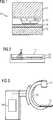
In der
Ebenfalls mittels derartiger Technologie wird eine buried oxide(BOX)-Schicht auf den Siliziumwafer aufgebracht. BOX-Schichten sind SiO2-Schichten unterhalb der Oberfläche des Substrats, die zum Beispiel mittels Ionenimplantation von sehr hohen Sauerstoffmengen in das Siliziumsubstrat eingebracht werden. Alternativ kann bei der Herstellung auch zuerst die Oxidschicht erstellt und anschließend die in der Epi-Si-Schicht eingebettete Photodiode aufgebracht werden. Die Dicke der Epi-Si-Schicht entspricht der Tiefe, in der die BOX-Schicht unterhalb der Oberfläche der Photodiode eingebracht ist.Also by such technology, a buried oxide (BOX) layer is deposited on the silicon wafer. BOX layers are SiO2 layers below the surface of the substrate, which are introduced into the silicon substrate by means of ion implantation of very high amounts of oxygen, for example. Alternatively, the oxide layer can also be created first during production and then the photodiode embedded in the epi-Si layer can be applied. The thickness of the Epi-Si layer corresponds to the depth at which the BOX layer is introduced below the surface of the photodiode.
Die Dicke der Epi-Si-Schicht wird bevorzugt angepasst an die Wellenlänge des Lichts, die die Szintillatorschicht bei der Absorption von Röntgenstrahlung erzeugt, gewählt. Sie wird dazu z. B. in einer derartigen Dicke gewählt, dass ein Großteil, zum Beispiel 90% bis 98% und insbesondere etwa 95%, des erzeugten Lichts absorbiert wird. Da die Wellenlänge des Lichts, die der Szintillator erzeugt, von dessen Materialzusammensetzung abhängig ist, ist jeweils eine genaue Anpassung zwischen dem Material des Szintillators und der Dicke der Photodioden/Epi-Si-Schicht vorteilhaft. Die BOX-Schicht selbst weist zum Beispiel eine Dicke zwischen 40 nm und 100 nm auf, um eine gute Isolierung gegenüber in dem Siliziumsubstrat
In der
Durch die Verwendung von CMOS-Technologie zur Herstellung der integrierten Photodiode ist eine schnelle und verlustfreie Umwandlung und Auslesen des elektrischen Messsignals gewährleistet. Bei einem derartigen Röntgendetektor erzeugen die Röntgenquanten im Bereich desselben Pixelelements ein Messsignal, in dem sie absorbiert werden. Einige Röntgenquanten, die versehentlich in dem Siliziumsubstrat absorbiert werden und dort aufgrund des Halbleitermaterials elektrische Ladungen erzeugen, können durch die von der BOX-Schicht erzeugte Isolierung nicht zu einem Störsignal beitragen. Der erfindungsgemäße Röntgendetektor gewährleistet also eine verbesserte und störungsfreiere Bildgebung, insbesondere auch bei Bildserien, die mit relativ niedriger Röntgendosis erstellt werden (sogenannte fluoro scenes).The use of CMOS technology to produce the integrated photodiode ensures fast and lossless conversion and readout of the electrical measurement signal. In such an X-ray detector, the X-ray quanta generate in the region of the same pixel element a measurement signal in which they are absorbed. Some X-ray quanta that are inadvertently absorbed in the silicon substrate and generate electrical charges there due to the semiconductor material can not contribute to a spurious signal due to the isolation produced by the BOX layer. The X-ray detector according to the invention therefore ensures improved and trouble-free imaging, in particular also for image series which are produced with a relatively low X-ray dose (so-called fluoro scenes).
In der
Die Erfindung lässt sich in folgender Weise kurz zusammenfassen: Für eine hochwertige Röntgenbildgebung ist ein Röntgendetektor mit einer aktiven Matrix aus Pixelelementen zur Detektion einer Röntgenstrahlung vorgesehen, wobei jedes Pixelelement eine Szintillatorschicht zur Umwandlung von Röntgenstrahlung in Licht und eine mittels CMOS-Technologie hergestellte Photodiode zur Umwandlung von Licht in ein elektrisches Messsignal aufweist, wobei die Pixelelemente auf einem Siliziumsubstrat angeordnet sind und zwischen dem Siliziumsubstrat und der Photodiode eine BOX(buried oxide)-Schicht angeordnet ist.The invention can be briefly summarized as follows: For high-quality X-ray imaging, an X-ray detector with an active matrix of pixel elements for detecting X-ray radiation is provided, each pixel element comprising a scintillator layer for converting X-radiation into light and a photodiode produced by CMOS technology for conversion of light in an electrical measurement signal, wherein the pixel elements are arranged on a silicon substrate and between the silicon substrate and the photodiode, a BOX (buried oxide) layer is arranged.
Claims (7)
Translated fromGermanPriority Applications (2)
| Application Number | Priority Date | Filing Date | Title |
|---|---|---|---|
| DE102011004936ADE102011004936A1 (en) | 2011-03-02 | 2011-03-02 | X-ray detector and medical X-ray device |
| US13/408,560US8785862B2 (en) | 2011-03-02 | 2012-02-29 | X-ray detector and medical X-ray device |
Applications Claiming Priority (1)
| Application Number | Priority Date | Filing Date | Title |
|---|---|---|---|
| DE102011004936ADE102011004936A1 (en) | 2011-03-02 | 2011-03-02 | X-ray detector and medical X-ray device |
Publications (1)
| Publication Number | Publication Date |
|---|---|
| DE102011004936A1true DE102011004936A1 (en) | 2012-09-06 |
Family
ID=46671236
Family Applications (1)
| Application Number | Title | Priority Date | Filing Date |
|---|---|---|---|
| DE102011004936ACeasedDE102011004936A1 (en) | 2011-03-02 | 2011-03-02 | X-ray detector and medical X-ray device |
Country Status (2)
| Country | Link |
|---|---|
| US (1) | US8785862B2 (en) |
| DE (1) | DE102011004936A1 (en) |
Families Citing this family (4)
| Publication number | Priority date | Publication date | Assignee | Title |
|---|---|---|---|---|
| US9935152B2 (en) | 2012-12-27 | 2018-04-03 | General Electric Company | X-ray detector having improved noise performance |
| US9917133B2 (en) | 2013-12-12 | 2018-03-13 | General Electric Company | Optoelectronic device with flexible substrate |
| WO2015138329A1 (en) | 2014-03-13 | 2015-09-17 | General Electric Company | Curved digital x-ray detector for weld inspection |
| DE102014205841A1 (en)* | 2014-03-28 | 2015-05-21 | Siemens Aktiengesellschaft | Image processing method for removing bright-burn artifacts and X-ray machine |
Citations (4)
| Publication number | Priority date | Publication date | Assignee | Title |
|---|---|---|---|---|
| US5354695A (en)* | 1992-04-08 | 1994-10-11 | Leedy Glenn J | Membrane dielectric isolation IC fabrication |
| DE19743523A1 (en)* | 1997-10-01 | 1999-04-15 | Siemens Ag | X=ray image converter with reset light source e.g. for medical diagnostic imaging |
| DE19944731A1 (en)* | 1999-09-17 | 2001-04-12 | Siemens Ag | Image detector for electromagnetic radiation is structured in such a way that insulating regions are formed between individual metal electrodes in a photodiode layer |
| US20050157841A1 (en)* | 2004-01-15 | 2005-07-21 | Nasreen Chopra | Three-dimensional x-ray imaging system |
Family Cites Families (11)
| Publication number | Priority date | Publication date | Assignee | Title |
|---|---|---|---|---|
| US4870667A (en)* | 1985-08-29 | 1989-09-26 | Picker International, Inc. | Radiation detector |
| SE513536C2 (en)* | 1999-01-21 | 2000-09-25 | Christer Froejdh | Arrangement for an X-ray pixel detector device and apparatus for an X-ray imaging arrangement |
| DE19934768A1 (en)* | 1999-07-23 | 2001-01-25 | Philips Corp Intellectual Pty | Detector for the detection of electromagnetic radiation |
| US7161155B1 (en)* | 2003-07-02 | 2007-01-09 | Analogic Corporation | X-ray detector with increased detective quantum efficiency |
| US8039882B2 (en)* | 2003-08-22 | 2011-10-18 | Micron Technology, Inc. | High gain, low noise photodiode for image sensors and method of formation |
| US6969899B2 (en)* | 2003-12-08 | 2005-11-29 | Taiwan Semiconductor Manufacturing Co., Ltd. | Image sensor with light guides |
| KR20070069191A (en)* | 2004-10-05 | 2007-07-02 | 코닌클리즈케 필립스 일렉트로닉스 엔.브이. | Semiconductor devices |
| US7538351B2 (en)* | 2005-03-23 | 2009-05-26 | Taiwan Semiconductor Manufacturing Co., Ltd. | Method for forming an SOI structure with improved carrier mobility and ESD protection |
| US7151287B1 (en)* | 2005-03-25 | 2006-12-19 | Cypress Semiconductor Corporation | Minimizing the effect of directly converted x-rays in x-ray imagers |
| US20060289777A1 (en)* | 2005-06-29 | 2006-12-28 | Wen Li | Detector with electrically isolated pixels |
| US7974805B2 (en)* | 2008-10-14 | 2011-07-05 | ON Semiconductor Trading, Ltd | Image sensor and method |
- 2011
- 2011-03-02DEDE102011004936Apatent/DE102011004936A1/ennot_activeCeased
- 2012
- 2012-02-29USUS13/408,560patent/US8785862B2/ennot_activeExpired - Fee Related
Patent Citations (4)
| Publication number | Priority date | Publication date | Assignee | Title |
|---|---|---|---|---|
| US5354695A (en)* | 1992-04-08 | 1994-10-11 | Leedy Glenn J | Membrane dielectric isolation IC fabrication |
| DE19743523A1 (en)* | 1997-10-01 | 1999-04-15 | Siemens Ag | X=ray image converter with reset light source e.g. for medical diagnostic imaging |
| DE19944731A1 (en)* | 1999-09-17 | 2001-04-12 | Siemens Ag | Image detector for electromagnetic radiation is structured in such a way that insulating regions are formed between individual metal electrodes in a photodiode layer |
| US20050157841A1 (en)* | 2004-01-15 | 2005-07-21 | Nasreen Chopra | Three-dimensional x-ray imaging system |
Also Published As
| Publication number | Publication date |
|---|---|
| US8785862B2 (en) | 2014-07-22 |
| US20120223238A1 (en) | 2012-09-06 |
Similar Documents
| Publication | Publication Date | Title |
|---|---|---|
| DE69328447T2 (en) | SURFACE THIN-LAYER PIXEL MATRIX DETECTOR FOR DIGITAL IMAGE AND DOSIMETRY IONIZING RADIATION IN REAL-TIME | |
| EP2453263B1 (en) | Hybrid organic photodiodes | |
| DE102013200021B4 (en) | Method for calibrating a counting digital X-ray detector, X-ray systems for carrying out such a method and method for recording an X-ray image | |
| DE102016205818A1 (en) | Apparatus and method for detecting X-radiation | |
| DE102012202500A1 (en) | Digital X-ray detector for receiving X-ray image irradiated by object, has sensor surface that is provided with uniform matrix structure having constant pixel pitch, and opening is formed between adjacent detector or sensor modules | |
| DE69927522T2 (en) | RADIATION IMAGE SENSOR AND METHOD FOR THE PRODUCTION THEREOF | |
| DE102011004936A1 (en) | X-ray detector and medical X-ray device | |
| DE102010006452A1 (en) | Radiation converter material, beam converter, radiation detector, use of a radiation converter material and method for producing a radiation converter material | |
| DE102008051045B4 (en) | Direct radiation converter | |
| DE102006033716A1 (en) | X-ray diagnosis apparatus, with digital imaging, has a dosage measurement sensor using part of the scintillating light with a matrix of detection sensors | |
| DE10132924A1 (en) | Flat dynamic radiation detector | |
| DE102011089595A1 (en) | X-ray detector used for diagnostic investigation in e.g. surgery, has active matrix layers that include pixel elements which have electrical switching element for converting light into image information | |
| DE102020202855A1 (en) | Anti-scatter collimator and method of making an anti-scatter collimator | |
| DE102011004918B4 (en) | Radiation detector, in particular X-ray detector | |
| DE102012213411B4 (en) | Method for the detection of X-radiation | |
| Starman et al. | A forward bias method for lag correction of an a‐Si flat panel detector | |
| DE102009060315A1 (en) | Counting x-ray detector | |
| DE112010005764B4 (en) | Radiation detector calibration using voltage injection | |
| DE102006042484A1 (en) | Radiation detector e.g. flat image detector, for e.g. X-ray radiography, has lens array with micro lenses arranged between scintillator plate and photo sensor, where lenses are partially designed as convex lenses | |
| DE2946108C2 (en) | Radiation detector | |
| DE102005056048B4 (en) | Flat panel detector | |
| DE102011080892B3 (en) | Direct conversion type x-ray detector for use in computed tomography system, has scintillation layer that is arranged on x-ray radiation facing side of semiconductor, and is made of material with specific decay time | |
| DE10137012B4 (en) | X-ray diagnostic device with a planar solid-state X-ray image converter | |
| DE102011004589B4 (en) | X-ray detector, comprising a plurality of sensor elements | |
| DE102011077195A1 (en) | Medical X-ray detector used in e.g. interventional radiology, has structural layer that is arranged between scintillator and active matrix so that light is indirectly provided to light-sensitive photodiode area of pixel element |
Legal Events
| Date | Code | Title | Description |
|---|---|---|---|
| R012 | Request for examination validly filed | ||
| R079 | Amendment of ipc main class | Free format text:PREVIOUS MAIN CLASS: H01L0027146000 Ipc:H05G0001640000 | |
| R016 | Response to examination communication | ||
| R002 | Refusal decision in examination/registration proceedings | ||
| R003 | Refusal decision now final | Effective date:20130111 |