DE102011002458A1 - Electronic assembly with improved thermal management - Google Patents
Electronic assembly with improved thermal managementDownload PDFInfo
- Publication number
- DE102011002458A1 DE102011002458A1DE102011002458ADE102011002458ADE102011002458A1DE 102011002458 A1DE102011002458 A1DE 102011002458A1DE 102011002458 ADE102011002458 ADE 102011002458ADE 102011002458 ADE102011002458 ADE 102011002458ADE 102011002458 A1DE102011002458 A1DE 102011002458A1
- Authority
- DE
- Germany
- Prior art keywords
- connecting element
- leadframe
- composite material
- assembly according
- semiconductor device
- Prior art date
- Legal status (The legal status is an assumption and is not a legal conclusion. Google has not performed a legal analysis and makes no representation as to the accuracy of the status listed.)
- Withdrawn
Links
- 239000004065semiconductorSubstances0.000claimsabstractdescription46
- 239000002131composite materialSubstances0.000claimsabstractdescription31
- 238000001465metallisationMethods0.000claimsabstractdescription10
- 239000000463materialSubstances0.000claimsdescription5
- 229910002804graphiteInorganic materials0.000claimsdescription4
- 239000010439graphiteSubstances0.000claimsdescription4
- 238000004080punchingMethods0.000claimsdescription4
- RYGMFSIKBFXOCR-UHFFFAOYSA-NCopperChemical compound[Cu]RYGMFSIKBFXOCR-UHFFFAOYSA-N0.000claimsdescription3
- 229910052802copperInorganic materials0.000claimsdescription3
- 239000010949copperSubstances0.000claimsdescription3
- OKTJSMMVPCPJKN-UHFFFAOYSA-NCarbonChemical compound[C]OKTJSMMVPCPJKN-UHFFFAOYSA-N0.000claimsdescription2
- ZOKXTWBITQBERF-UHFFFAOYSA-NMolybdenumChemical compound[Mo]ZOKXTWBITQBERF-UHFFFAOYSA-N0.000claims1
- 229910052750molybdenumInorganic materials0.000claims1
- 239000011733molybdenumSubstances0.000claims1
- 239000002245particleSubstances0.000description8
- 238000004519manufacturing processMethods0.000description5
- 238000000034methodMethods0.000description4
- 230000006978adaptationEffects0.000description3
- 239000006185dispersionSubstances0.000description3
- 230000017525heat dissipationEffects0.000description3
- 229910052751metalInorganic materials0.000description3
- 239000002184metalSubstances0.000description3
- 239000000203mixtureSubstances0.000description3
- 239000000919ceramicSubstances0.000description2
- 239000011362coarse particleSubstances0.000description2
- 230000008646thermal stressEffects0.000description2
- 230000000930thermomechanical effectEffects0.000description2
- 230000000712assemblyEffects0.000description1
- 238000000429assemblyMethods0.000description1
- WUUZKBJEUBFVMV-UHFFFAOYSA-Ncopper molybdenumChemical compound[Cu].[Mo]WUUZKBJEUBFVMV-UHFFFAOYSA-N0.000description1
- 230000006378damageEffects0.000description1
- 230000001419dependent effectEffects0.000description1
- 238000011161developmentMethods0.000description1
- 230000018109developmental processEffects0.000description1
- 239000003792electrolyteSubstances0.000description1
- 238000009713electroplatingMethods0.000description1
- 239000000446fuelSubstances0.000description1
- 239000008187granular materialSubstances0.000description1
- 230000005484gravityEffects0.000description1
- 238000002955isolationMethods0.000description1
- 239000007769metal materialSubstances0.000description1
- 238000002360preparation methodMethods0.000description1
- 238000005476solderingMethods0.000description1
- 230000035882stressEffects0.000description1
- 239000000758substrateSubstances0.000description1
Images
Classifications
- H—ELECTRICITY
- H01—ELECTRIC ELEMENTS
- H01L—SEMICONDUCTOR DEVICES NOT COVERED BY CLASS H10
- H01L23/00—Details of semiconductor or other solid state devices
- H01L23/48—Arrangements for conducting electric current to or from the solid state body in operation, e.g. leads, terminal arrangements ; Selection of materials therefor
- H01L23/488—Arrangements for conducting electric current to or from the solid state body in operation, e.g. leads, terminal arrangements ; Selection of materials therefor consisting of soldered or bonded constructions
- H01L23/495—Lead-frames or other flat leads
- H01L23/49568—Lead-frames or other flat leads specifically adapted to facilitate heat dissipation
- H—ELECTRICITY
- H01—ELECTRIC ELEMENTS
- H01L—SEMICONDUCTOR DEVICES NOT COVERED BY CLASS H10
- H01L23/00—Details of semiconductor or other solid state devices
- H01L23/34—Arrangements for cooling, heating, ventilating or temperature compensation ; Temperature sensing arrangements
- H01L23/42—Fillings or auxiliary members in containers or encapsulations selected or arranged to facilitate heating or cooling
- H01L23/433—Auxiliary members in containers characterised by their shape, e.g. pistons
- H01L23/4334—Auxiliary members in encapsulations
- H—ELECTRICITY
- H01—ELECTRIC ELEMENTS
- H01L—SEMICONDUCTOR DEVICES NOT COVERED BY CLASS H10
- H01L23/00—Details of semiconductor or other solid state devices
- H01L23/48—Arrangements for conducting electric current to or from the solid state body in operation, e.g. leads, terminal arrangements ; Selection of materials therefor
- H01L23/488—Arrangements for conducting electric current to or from the solid state body in operation, e.g. leads, terminal arrangements ; Selection of materials therefor consisting of soldered or bonded constructions
- H01L23/495—Lead-frames or other flat leads
- H01L23/49503—Lead-frames or other flat leads characterised by the die pad
- H—ELECTRICITY
- H01—ELECTRIC ELEMENTS
- H01L—SEMICONDUCTOR DEVICES NOT COVERED BY CLASS H10
- H01L23/00—Details of semiconductor or other solid state devices
- H01L23/48—Arrangements for conducting electric current to or from the solid state body in operation, e.g. leads, terminal arrangements ; Selection of materials therefor
- H01L23/488—Arrangements for conducting electric current to or from the solid state body in operation, e.g. leads, terminal arrangements ; Selection of materials therefor consisting of soldered or bonded constructions
- H01L23/495—Lead-frames or other flat leads
- H01L23/49541—Geometry of the lead-frame
- H01L23/49562—Geometry of the lead-frame for individual devices of subclass H10D
- H—ELECTRICITY
- H01—ELECTRIC ELEMENTS
- H01L—SEMICONDUCTOR DEVICES NOT COVERED BY CLASS H10
- H01L24/00—Arrangements for connecting or disconnecting semiconductor or solid-state bodies; Methods or apparatus related thereto
- H01L24/01—Means for bonding being attached to, or being formed on, the surface to be connected, e.g. chip-to-package, die-attach, "first-level" interconnects; Manufacturing methods related thereto
- H01L24/26—Layer connectors, e.g. plate connectors, solder or adhesive layers; Manufacturing methods related thereto
- H01L24/31—Structure, shape, material or disposition of the layer connectors after the connecting process
- H01L24/32—Structure, shape, material or disposition of the layer connectors after the connecting process of an individual layer connector
- H—ELECTRICITY
- H01—ELECTRIC ELEMENTS
- H01L—SEMICONDUCTOR DEVICES NOT COVERED BY CLASS H10
- H01L2224/00—Indexing scheme for arrangements for connecting or disconnecting semiconductor or solid-state bodies and methods related thereto as covered by H01L24/00
- H01L2224/01—Means for bonding being attached to, or being formed on, the surface to be connected, e.g. chip-to-package, die-attach, "first-level" interconnects; Manufacturing methods related thereto
- H01L2224/26—Layer connectors, e.g. plate connectors, solder or adhesive layers; Manufacturing methods related thereto
- H01L2224/31—Structure, shape, material or disposition of the layer connectors after the connecting process
- H01L2224/32—Structure, shape, material or disposition of the layer connectors after the connecting process of an individual layer connector
- H01L2224/321—Disposition
- H01L2224/32151—Disposition the layer connector connecting between a semiconductor or solid-state body and an item not being a semiconductor or solid-state body, e.g. chip-to-substrate, chip-to-passive
- H01L2224/32221—Disposition the layer connector connecting between a semiconductor or solid-state body and an item not being a semiconductor or solid-state body, e.g. chip-to-substrate, chip-to-passive the body and the item being stacked
- H01L2224/32245—Disposition the layer connector connecting between a semiconductor or solid-state body and an item not being a semiconductor or solid-state body, e.g. chip-to-substrate, chip-to-passive the body and the item being stacked the item being metallic
- H—ELECTRICITY
- H01—ELECTRIC ELEMENTS
- H01L—SEMICONDUCTOR DEVICES NOT COVERED BY CLASS H10
- H01L2924/00—Indexing scheme for arrangements or methods for connecting or disconnecting semiconductor or solid-state bodies as covered by H01L24/00
- H01L2924/10—Details of semiconductor or other solid state devices to be connected
- H01L2924/11—Device type
- H01L2924/13—Discrete devices, e.g. 3 terminal devices
- H01L2924/1304—Transistor
- H01L2924/1305—Bipolar Junction Transistor [BJT]
- H01L2924/13055—Insulated gate bipolar transistor [IGBT]
- H—ELECTRICITY
- H01—ELECTRIC ELEMENTS
- H01L—SEMICONDUCTOR DEVICES NOT COVERED BY CLASS H10
- H01L2924/00—Indexing scheme for arrangements or methods for connecting or disconnecting semiconductor or solid-state bodies as covered by H01L24/00
- H01L2924/10—Details of semiconductor or other solid state devices to be connected
- H01L2924/11—Device type
- H01L2924/13—Discrete devices, e.g. 3 terminal devices
- H01L2924/1304—Transistor
- H01L2924/1306—Field-effect transistor [FET]
- H01L2924/13091—Metal-Oxide-Semiconductor Field-Effect Transistor [MOSFET]
- H—ELECTRICITY
- H01—ELECTRIC ELEMENTS
- H01L—SEMICONDUCTOR DEVICES NOT COVERED BY CLASS H10
- H01L2924/00—Indexing scheme for arrangements or methods for connecting or disconnecting semiconductor or solid-state bodies as covered by H01L24/00
- H01L2924/30—Technical effects
- H01L2924/35—Mechanical effects
- H01L2924/351—Thermal stress
Landscapes
- Engineering & Computer Science (AREA)
- Computer Hardware Design (AREA)
- Microelectronics & Electronic Packaging (AREA)
- Power Engineering (AREA)
- Physics & Mathematics (AREA)
- Condensed Matter Physics & Semiconductors (AREA)
- General Physics & Mathematics (AREA)
- Lead Frames For Integrated Circuits (AREA)
- Cooling Or The Like Of Semiconductors Or Solid State Devices (AREA)
Abstract
Translated fromGermanDescription
Translated fromGermanStand der TechnikState of the art
Die vorliegende Erfindung betrifft eine elektronische Baugruppe mit verbessertem Thermo-Management durch lokal angepasste, verbesserte thermo-mechanische Stabilität.The present invention relates to an electronic assembly with improved thermal management by locally adapted, improved thermo-mechanical stability.
Elektronische Baugruppen sind aus dem Stand der Technik bekannt, wobei speziell in Niedervolt-Anwendungen Leistungshalbleiter direkt auf Substrate, insbesondere Leadframes, gelötet werden. Derartige elektronische Bauteile weisen gute thermische Eigenschaften auf, da Wärme vom Leistungshalbleiter direkt auf das Leadframe übertragen werden kann und das Leadframe die Wärme dann schnell vom Leistungshalbleiter fortleitet. Ein großer Nachteil dieser direkt kontaktierten elektronischen Bauteile resultiert jedoch aus den großen Unterschieden zwischen den Wärmeausdehnungskoeffizienten des Leistungshalbleiters und des Leadframes, üblicherweise ein Metallblech. Hieraus können thermo-mechanische Spannungen zwischen Leadframe und Leistungshalbleiter resultieren, was im Extremfall zu einer Zerstörung des Bauteils führt.Electronic assemblies are known from the prior art, in particular in low-voltage applications power semiconductors are soldered directly to substrates, in particular lead frames. Such electronic components have good thermal properties, since heat from the power semiconductor can be transferred directly to the leadframe and the leadframe then quickly conducts the heat away from the power semiconductor. However, a major disadvantage of these directly contacted electronic components results from the large differences between the thermal expansion coefficients of the power semiconductor and the lead frame, usually a metal sheet. This can result in thermo-mechanical stresses between the leadframe and the power semiconductor, which in extreme cases leads to destruction of the component.
Offenbarung der ErfindungDisclosure of the invention
Die elektronische Baugruppe mit den Merkmalen des Anspruchs 1 weist demgegenüber den Vorteil auf, dass zwischen einem Leadframe und einem Halbleiterbauelement stark reduzierte, thermisch basierte Spannungen möglich sind, so dass eine Lebensdauer der elektronischen Baugruppe signifikant verlängert werden kann. Darüber hinaus kann die erfindungsgemäße elektronische Baugruppe trotzdem sehr kostengünstig und in Serienfertigung hergestellt werden. Insbesondere kann im Vergleich mit einer Direktbestückung des Leadframes mit Halbleiterbauelementen nur eine minimale Kostensteigerung auftreten, da erfindungsgemäß ein elektrisch leitendes Verbindungselement nur lokal im Bereich des Halbleiterbauelements vorgesehen ist. Das elektrisch leitende Verbindungselement ist dabei aus einem Verbundmaterial hergestellt, wobei eine lötbare Metallisierung auf einer zum Halbleiterbauelement gerichteten Oberfläche vorgesehen ist. Somit wird erfindungsgemäß das Verbindungselement für die Wärmeübertragung von dem Halbleiterbauelement auf das Leadframe zwischengeschaltet. Eine Wärmeleitfähigkeit des Verbindungselements liegt dabei zwischen der des Halbleiterbauelements und der des Leadframes. Ferner wird es erfindungsgemäß möglich, die elektronische Baugruppe nicht nur bei Niedervolt-Anwendungen, sondern auch bei Hochleistungs-Anwendungen einzusetzen, bei denen das Halbleiterbauelement viel Wärme erzeugt. Erfindungsgemäß kann somit immer noch ein einfach und kostengünstig herstellbares Leadframe verwendet werden, wobei das Verbindungselement aus einem Verbundmaterial einen großen Variationsspielraum hinsichtlich der Zusammensetzung, der Schichtdicke usw., ermöglicht.In contrast, the electronic module with the features of
Die Unteransprüche zeigen bevorzugte Weiterbildungen der Erfindung.The dependent claims show preferred developments of the invention.
Vorzugsweise ist eine Fläche des lokal vorgesehenen Verbindungselements maximal doppelt so groß wie eine Fläche des Halbleiterbauelements. Hierdurch kann einerseits eine gute Wärmeableitung vom Halbleiterbauelement ermöglicht werden und andererseits bleiben die Kosten zur Herstellung des Verbindungselements und der für das Verbindungselement notwendige Platzbedarf im Rahmen. Besonders bevorzugt ist dabei eine Fläche des Verbindungselements gleich groß wie eine Fläche des Halbleiterbauelements, um eine Wärmeableitung von einer gesamten Unterfläche des Halbleiterbauelements sicherzustellen.Preferably, a surface of the locally provided connection element is at most twice as large as a surface of the semiconductor component. In this way, on the one hand, good heat dissipation from the semiconductor component can be made possible and, on the other hand, the costs for producing the connecting element and the space required for the connecting element remain within the framework. Particularly preferably, an area of the connecting element is the same size as a surface of the semiconductor component in order to ensure heat dissipation from an entire lower surface of the semiconductor component.
Gemäß einem bevorzugten Ausführungsbeispiel der Erfindung weist das Leadframe vorzugsweise eine Ausstanzung auf, in welcher das Verbindungselement angeordnet ist. Die Ausstanzung ist dabei an einer Position vorgesehen, an welcher in der später fertiggestellten elektronischen Baugruppe ein Halbleiterbauelement angeordnet ist. Die Ausstanzung wird gleichzeitig mit der Herstellung des Leadframes erzeugt und verursacht somit keinerlei Zusatzkosten. Ferner definiert die Ausstanzung die Position des Verbindungselements, so dass dieses schnell und einfach in dem Leadframe angeordnet werden kann. Weiter steht das Verbindungselement dadurch nicht oder nur in geringem Umfang von einer Oberfläche des Leadframes vor, so dass eine kompakte elektronische Baugruppe möglich ist.According to a preferred embodiment of the invention, the leadframe preferably has a punched-out, in which the connecting element is arranged. The punched-out is provided at a position at which a semiconductor component is arranged in the later completed electronic assembly. The punching is produced simultaneously with the production of the leadframe and thus causes no additional costs. Further, the punch defines the position of the connector so that it can be quickly and easily placed in the leadframe. Furthermore, the connecting element is not in front or only to a small extent from a surface of the leadframe, so that a compact electronic assembly is possible.
Eine Dicke des Verbindungselements ist vorzugsweise gleich einer Dicke des Leadframes. Somit ersetzt das Verbindungselement das ausgestanzte Material aus dem Leadframe, ohne dass ein Halbleiterbauelement dadurch übermäßig erhöht zu einer Oberfläche des Leadframes angeordnet ist.A thickness of the connecting element is preferably equal to a thickness of the leadframe. Thus, the connector replaces the stamped material from the leadframe without excessively increasing a semiconductor device to a surface of the leadframe.
Gemäß einer bevorzugten Ausgestaltung der Erfindung weist das Leadframe eine vertiefte Einprägung auf, wobei das Verbundelement in der Einprägung angeordnet ist. Somit wird eine Einprägung vorgesehen, was die Herstellungskosten des Leadframes ebenfalls nicht signifikant vergrößert, da die Vertiefung gleichzeitig mit dem Leadframe hergestellt wird. Die Einprägung dient dann als Tasche zur Aufnahme des Verbindungselements, wodurch ebenfalls eine überhöhte Anordnung des auf dem Verbindungselement angeordneten Halbleiterbauelements vermieden wird.According to a preferred embodiment of the invention, the leadframe on a recessed impression, wherein the composite element is arranged in the imprint. Thus, an embossment is provided, which also does not significantly increase the manufacturing costs of the leadframe, since the depression is produced simultaneously with the leadframe. The imprint then serves as a pocket for receiving the connecting element, which also avoids an excessive arrangement of the semiconductor component arranged on the connecting element.
Besonders bevorzugt ist eine Oberfläche des Leadframes bündig mit einer Oberfläche des Verbindungselements. Particularly preferably, a surface of the leadframe is flush with a surface of the connecting element.
Besonders bevorzugt wird das Verbindungselement als vorbereitetes Bauteil vorgesehen, so dass das Verbindungselement lediglich noch am Leadframe angeordnet werden muss.Particularly preferably, the connecting element is provided as a prepared component, so that the connecting element only has to be arranged on the leadframe.
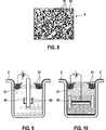
Für eine besonders schnelle und kostengünstige Herstellbarkeit ist zwischen dem Verbindungselement und dem Leadframe eine Presspassung vorgesehen. Die Presspassung kann dabei sowohl an der Ausstanzung als auch an der Einprägung vorgesehen werden. Alternativ oder zusätzlich ist zwischen dem Verbindungselement und dem Leadframe eine stoffschlüssige Verbindung vorgesehen. Besonders bevorzugt wird die stoffschlüssige Verbindung mittels eines Galvanikprozesses hergestellt. Hierbei ist das Verbindungselement als galvanische Dispersionsschicht im lokal begrenzten Bereich vorgesehen. Hierzu werden Fremdpartikel in einem Galvanikbad eingebracht, welche dann während des Galvanikprozesses in die wachsende Schicht eingebaut werden. Besonders bevorzugt werden dabei sehr grobe Partikel in die Aussparung bzw. in die Vertiefung eingelegt und eine metallische Schicht wächst um diese Partikel herum, bis das Verbindungselement hergestellt ist.For a particularly fast and cost-effective manufacturability, a press fit is provided between the connecting element and the leadframe. The interference fit can be provided both on the punching and on the impression. Alternatively or additionally, a cohesive connection is provided between the connecting element and the leadframe. Particularly preferably, the cohesive connection is produced by means of a galvanic process. Here, the connecting element is provided as a galvanic dispersion layer in the localized area. For this purpose, foreign particles are introduced into a galvanic bath, which are then incorporated into the growing layer during the electroplating process. In this case, very coarse particles are particularly preferably inserted into the recess or into the depression, and a metallic layer grows around these particles until the connecting element is produced.
Besonders bevorzugt weist das Verbindungselement als Verbundmaterial einen Kupfer-Molybdän-Verbund oder einen Kupfer-Graphit-Verbund auf.Particularly preferably, the connecting element as a composite material on a copper-molybdenum composite or a copper-graphite composite.
Besonders bevorzugt weist das Verbindungselement einen. Wärmeleitkoeffizienten im Bereich von 100 bis 900 W/mk auf.Particularly preferably, the connecting element has a. Wärmeleitkoeffizienten in the range of 100 to 900 W / mk on.
Das Halbleiterbauelement ist vorzugsweise ein FET, insbesondere eine MOSFET, oder ein IGBT.The semiconductor component is preferably a FET, in particular a MOSFET, or an IGBT.
Die erfindungsgemäße elektronische Baugruppe wird besonders bevorzugt in Fahrzeugen als Leistungsmodul eingesetzt. Hierbei kann die erfindungsgemäße elektronische Baugruppe im Antriebsbereich und/oder im Energiemanagement, insbesondere auch bei Hybridfahrzeugen, Brennstoffzellenfahrzeugen und Elektrofahrzeugen verwendet werden. Auch im Bereich von regenerativer Energie, beispielsweise bei Photovoltaikinvertern, kann die erfindungsgemäße elektronische Baugruppe verwendet werden.The electronic assembly according to the invention is particularly preferably used in vehicles as a power module. In this case, the electronic assembly according to the invention in the drive area and / or energy management, especially in hybrid vehicles, fuel cell vehicles and electric vehicles can be used. Also in the field of renewable energy, such as photovoltaic inverters, the electronic assembly according to the invention can be used.
Zeichnungdrawing
Nachfolgend werden bevorzugte Ausführungsbeispiele der Erfindung unter Bezugnahme auf die begleitende Zeichnung im Detail beschrieben. In der Zeichnung ist:Hereinafter, preferred embodiments of the invention will be described in detail with reference to the accompanying drawings. In the drawing is:
Bevorzugte Ausführungsformen der ErfindungPreferred embodiments of the invention
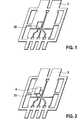
Nachfolgend wird unter Bezugnahme auf die
Wie insbesondere aus
Eine Fläche des Verbindungselements
Die Wärmeausdehnungskoeffizienten des Verbindungselements
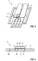
Nachfolgend wird unter Bezugnahme auf die
Wie insbesondere aus
Die Einprägungen
Die
Somit kann auch beim zweiten Ausführungsbeispiel lokal ein Verbindungselement
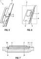
Es sei angemerkt, dass es erfindungsgemäß auch möglich ist, dass ein Verbindungselement
Alternativ ist es auch möglich, dass das erfindungsgemäße Verbundmaterial derart hergestellt wird, indem es großflächig auf einer Basis abgeschieden wird und dann entsprechend der jeweils gewünschten Größe vereinzelt wird und anschließend, wie im ersten Ausführungsbeispiel beschrieben, in entsprechend gebildete Ausstanzungen eingesetzt werden.Alternatively, it is also possible for the composite material according to the invention to be produced in such a way that it is deposited over a large area on a base and then singulated according to the particular desired size and then, as described in the first exemplary embodiment, be inserted into correspondingly formed cut-outs.
Claims (10)
Translated fromGermanPriority Applications (6)
| Application Number | Priority Date | Filing Date | Title |
|---|---|---|---|
| DE102011002458ADE102011002458A1 (en) | 2011-01-05 | 2011-01-05 | Electronic assembly with improved thermal management |
| JP2013547827AJP2014502059A (en) | 2011-01-05 | 2011-11-11 | Electronic assembly with improved thermal management |
| CN2011800641132ACN103283017A (en) | 2011-01-05 | 2011-11-11 | Electronic assembly with improved thermal management |
| US13/978,436US8933546B2 (en) | 2011-01-05 | 2011-11-11 | Electronic assembly with improved thermal management |
| EP11790899.6AEP2661770A1 (en) | 2011-01-05 | 2011-11-11 | Electronic assembly with improved thermal management |
| PCT/EP2011/069955WO2012092994A1 (en) | 2011-01-05 | 2011-11-11 | Electronic assembly with improved thermal management |
Applications Claiming Priority (1)
| Application Number | Priority Date | Filing Date | Title |
|---|---|---|---|
| DE102011002458ADE102011002458A1 (en) | 2011-01-05 | 2011-01-05 | Electronic assembly with improved thermal management |
Publications (1)
| Publication Number | Publication Date |
|---|---|
| DE102011002458A1true DE102011002458A1 (en) | 2012-07-05 |
Family
ID=45093702
Family Applications (1)
| Application Number | Title | Priority Date | Filing Date |
|---|---|---|---|
| DE102011002458AWithdrawnDE102011002458A1 (en) | 2011-01-05 | 2011-01-05 | Electronic assembly with improved thermal management |
Country Status (6)
| Country | Link |
|---|---|
| US (1) | US8933546B2 (en) |
| EP (1) | EP2661770A1 (en) |
| JP (1) | JP2014502059A (en) |
| CN (1) | CN103283017A (en) |
| DE (1) | DE102011002458A1 (en) |
| WO (1) | WO2012092994A1 (en) |
Families Citing this family (2)
| Publication number | Priority date | Publication date | Assignee | Title |
|---|---|---|---|---|
| JP2021180230A (en)* | 2020-05-13 | 2021-11-18 | ローム株式会社 | Semiconductor device |
| CN120493594B (en)* | 2025-07-21 | 2025-09-09 | 五源(南通)航天科技有限公司 | A fuel cell test stand design method and system |
Citations (2)
| Publication number | Priority date | Publication date | Assignee | Title |
|---|---|---|---|---|
| US4700273A (en)* | 1986-06-03 | 1987-10-13 | Kaufman Lance R | Circuit assembly with semiconductor expansion matched thermal path |
| US6114048A (en)* | 1998-09-04 | 2000-09-05 | Brush Wellman, Inc. | Functionally graded metal substrates and process for making same |
Family Cites Families (18)
| Publication number | Priority date | Publication date | Assignee | Title |
|---|---|---|---|---|
| JPS4940868A (en)* | 1972-08-25 | 1974-04-17 | ||
| JPS5670650U (en)* | 1979-10-31 | 1981-06-11 | ||
| JPS5670650A (en)* | 1979-11-13 | 1981-06-12 | Nec Corp | Semiconductor device |
| JPS5921032A (en)* | 1982-07-26 | 1984-02-02 | Sumitomo Electric Ind Ltd | Substrate for semiconductor device |
| JPH0231863A (en) | 1987-11-18 | 1990-02-01 | Nordson Kk | Method for applying and maturating coating material |
| US5202288A (en)* | 1990-06-01 | 1993-04-13 | Robert Bosch Gmbh | Method of manufacturing an electronic circuit component incorporating a heat sink |
| DE4017697C2 (en)* | 1990-06-01 | 2003-12-11 | Bosch Gmbh Robert | Electronic component, process for its production and use |
| JPH04329660A (en)* | 1991-04-30 | 1992-11-18 | Oki Electric Ind Co Ltd | Lead frame and manufacture thereof |
| JPH04359458A (en)* | 1991-06-05 | 1992-12-11 | Mitsubishi Electric Corp | Semiconductor device |
| JPH0940868A (en) | 1995-07-27 | 1997-02-10 | Toray Dow Corning Silicone Co Ltd | Thermosetting silicon rubber composition |
| JP3690171B2 (en) | 1999-03-16 | 2005-08-31 | 株式会社日立製作所 | Composite material and its production method and application |
| EP1403923A1 (en)* | 2002-09-27 | 2004-03-31 | Abb Research Ltd. | Press pack power semiconductor module |
| JP4329660B2 (en) | 2004-09-21 | 2009-09-09 | カシオ計算機株式会社 | Light source device and projector |
| DE102004063544A1 (en)* | 2004-12-30 | 2006-07-13 | Robert Bosch Gmbh | Structured carrier strip |
| US7446411B2 (en)* | 2005-10-24 | 2008-11-04 | Freescale Semiconductor, Inc. | Semiconductor structure and method of assembly |
| JP2007142126A (en) | 2005-11-18 | 2007-06-07 | Allied Material Corp | Composite material and semiconductor-mounted heat dissipation substrate, and ceramic package using the same |
| JP4764983B2 (en)* | 2006-07-25 | 2011-09-07 | 富士電機株式会社 | Manufacturing method of semiconductor device |
| US7898807B2 (en)* | 2009-03-09 | 2011-03-01 | General Electric Company | Methods for making millichannel substrate, and cooling device and apparatus using the substrate |
- 2011
- 2011-01-05DEDE102011002458Apatent/DE102011002458A1/ennot_activeWithdrawn
- 2011-11-11CNCN2011800641132Apatent/CN103283017A/enactivePending
- 2011-11-11USUS13/978,436patent/US8933546B2/ennot_activeExpired - Fee Related
- 2011-11-11WOPCT/EP2011/069955patent/WO2012092994A1/enactiveApplication Filing
- 2011-11-11EPEP11790899.6Apatent/EP2661770A1/ennot_activeWithdrawn
- 2011-11-11JPJP2013547827Apatent/JP2014502059A/enactivePending
Patent Citations (2)
| Publication number | Priority date | Publication date | Assignee | Title |
|---|---|---|---|---|
| US4700273A (en)* | 1986-06-03 | 1987-10-13 | Kaufman Lance R | Circuit assembly with semiconductor expansion matched thermal path |
| US6114048A (en)* | 1998-09-04 | 2000-09-05 | Brush Wellman, Inc. | Functionally graded metal substrates and process for making same |
Also Published As
| Publication number | Publication date |
|---|---|
| US8933546B2 (en) | 2015-01-13 |
| US20130277812A1 (en) | 2013-10-24 |
| CN103283017A (en) | 2013-09-04 |
| WO2012092994A1 (en) | 2012-07-12 |
| EP2661770A1 (en) | 2013-11-13 |
| JP2014502059A (en) | 2014-01-23 |
Similar Documents
| Publication | Publication Date | Title |
|---|---|---|
| DE102011085282B4 (en) | Corrosion-protected semiconductor module and method for producing a corrosion-protected semiconductor module | |
| DE102009033321B4 (en) | Power semiconductor device | |
| DE102009011233B4 (en) | Method for producing a semiconductor device | |
| DE102010038727B4 (en) | Power semiconductor module and method for producing a power semiconductor module | |
| DE102013102829B4 (en) | Power semiconductor module and arrangement hereby | |
| DE102010044709A1 (en) | Power semiconductor module with metal sintering, preferably silver sintered compounds and manufacturing method | |
| DE102013219833A1 (en) | SEMICONDUCTOR MODULE WITH LADDER PLATE AND METHOD FOR HOLDING A SEMICONDUCTOR MODULE WITH A CONDUCTOR PLATE | |
| DE102009032973A1 (en) | Power semiconductor device | |
| EP2327286B1 (en) | Circuit housing having a heat coupling element | |
| DE102014213564A1 (en) | Semiconductor device and method for its production | |
| DE102011088218B4 (en) | Electronic power module with thermal coupling layers to a cooling element and method of manufacture | |
| DE102012222791A1 (en) | Method for contacting a semiconductor and semiconductor device with increased stability to thermomechanical influences | |
| DE102007037297A1 (en) | Circuit carrier structure with improved heat dissipation | |
| DE102008008141A1 (en) | Power semiconductor module and method for its production | |
| DE102004021054B4 (en) | Semiconductor component and method for its production | |
| DE102020111652A1 (en) | SEMICONDUCTOR ENCLOSURE WITH CONDUCTIVE CLIP WITH MULTIPLE LEVELS FOR COOLING THE TOP | |
| DE102016208029A1 (en) | Semiconductor device | |
| DE102016104844A1 (en) | Method for producing a chip composite | |
| DE102012214917A1 (en) | Semiconductor device and method for its production | |
| DE102013209444A1 (en) | Power semiconductor module, method for operating a power semiconductor module and method for producing a power semiconductor module | |
| EP3555913A1 (en) | Semiconductor module having a base plate with a concave curvature | |
| DE102011002458A1 (en) | Electronic assembly with improved thermal management | |
| DE102013219433B4 (en) | Electronic power module with elastic contacts and stack construction with such a power module | |
| DE102015204905A1 (en) | Electronic control device | |
| DE102011086687A1 (en) | Method for contacting a semiconductor and contact arrangement for a semiconductor |
Legal Events
| Date | Code | Title | Description |
|---|---|---|---|
| R163 | Identified publications notified | ||
| R119 | Application deemed withdrawn, or ip right lapsed, due to non-payment of renewal fee |