DE102010063579A1 - Optical range finder has reset devices that are controlled so as to control discharge of accumulation gates when voltage of accumulation gates reaches or exceeds threshold value - Google Patents
Optical range finder has reset devices that are controlled so as to control discharge of accumulation gates when voltage of accumulation gates reaches or exceeds threshold valueDownload PDFInfo
- Publication number
- DE102010063579A1 DE102010063579A1DE201010063579DE102010063579ADE102010063579A1DE 102010063579 A1DE102010063579 A1DE 102010063579A1DE 201010063579DE201010063579DE 201010063579DE 102010063579 ADE102010063579 ADE 102010063579ADE 102010063579 A1DE102010063579 A1DE 102010063579A1
- Authority
- DE
- Germany
- Prior art keywords
- accumulation
- accumulation gates
- gates
- reset
- voltage
- Prior art date
- Legal status (The legal status is an assumption and is not a legal conclusion. Google has not performed a legal analysis and makes no representation as to the accuracy of the status listed.)
- Ceased
Links
- 238000009825accumulationMethods0.000titleclaimsabstractdescription69
- 230000003287optical effectEffects0.000titleclaimsabstractdescription17
- 230000010354integrationEffects0.000claimsdescription19
- 238000005286illuminationMethods0.000claimsdescription7
- 238000000034methodMethods0.000claimsdescription5
- 238000011017operating methodMethods0.000abstract1
- 239000003990capacitorSubstances0.000description14
- 238000005259measurementMethods0.000description6
- 230000010363phase shiftEffects0.000description6
- 238000010586diagramMethods0.000description4
- 230000000694effectsEffects0.000description4
- 230000004907fluxEffects0.000description4
- 239000002800charge carrierSubstances0.000description3
- 230000007423decreaseEffects0.000description3
- 238000007493shaping processMethods0.000description3
- 230000003247decreasing effectEffects0.000description2
- 230000003071parasitic effectEffects0.000description2
- BUHVIAUBTBOHAG-FOYDDCNASA-N(2r,3r,4s,5r)-2-[6-[[2-(3,5-dimethoxyphenyl)-2-(2-methylphenyl)ethyl]amino]purin-9-yl]-5-(hydroxymethyl)oxolane-3,4-diolChemical compoundCOC1=CC(OC)=CC(C(CNC=2C=3N=CN(C=3N=CN=2)[C@H]2[C@@H]([C@H](O)[C@@H](CO)O2)O)C=2C(=CC=CC=2)C)=C1BUHVIAUBTBOHAG-FOYDDCNASA-N0.000description1
- 230000002411adverseEffects0.000description1
- 230000005540biological transmissionEffects0.000description1
- 238000007599dischargingMethods0.000description1
- 230000005670electromagnetic radiationEffects0.000description1
- 238000003384imaging methodMethods0.000description1
- 230000005855radiationEffects0.000description1
Images


Classifications
- G—PHYSICS
- G01—MEASURING; TESTING
- G01C—MEASURING DISTANCES, LEVELS OR BEARINGS; SURVEYING; NAVIGATION; GYROSCOPIC INSTRUMENTS; PHOTOGRAMMETRY OR VIDEOGRAMMETRY
- G01C3/00—Measuring distances in line of sight; Optical rangefinders
- G01C3/02—Details
- G01C3/06—Use of electric means to obtain final indication
- G01C3/08—Use of electric radiation detectors
Landscapes
- Physics & Mathematics (AREA)
- Electromagnetism (AREA)
- Engineering & Computer Science (AREA)
- General Physics & Mathematics (AREA)
- Radar, Positioning & Navigation (AREA)
- Remote Sensing (AREA)
- Measurement Of Optical Distance (AREA)
- Optical Radar Systems And Details Thereof (AREA)
Abstract
Description
Translated fromGermanDie Erfindung betrifft einen optischen Entfernungsmesser mit mindestens zwei als Photomischdetektoren ausgebildeten Empfangspixeln nach Gattung des unabhängigen Anspruchs.The invention relates to an optical rangefinder with at least two receiving pixels designed as photonic mixer detectors according to the category of the independent claim.
Der erfindungsgemäße optische Entfernungsmesser betrifft Systeme, die Entfernungen aus der Lichtlaufzeit und insbesondere aus einer Phasenverschiebung einer emittierten und empfangenen Strahlung gewinnen. Bevorzugt sind Lichtlaufzeitsensoren mit Photomischdetektoren (PMD) geeignet, wie sie u. a. in den Anmeldungen
Aufgabe der Erfindung ist es, die Messgenauigkeit eines optischen Entfernungsmessers weiter zu verbessern.The object of the invention is to further improve the measurement accuracy of an optical rangefinder.
Die Aufgabe wird in vorteilhafter Weise durch den erfindungsgemäßen optischen Entfernungsmesser des unabhängigen Anspruchs gelöst.The object is achieved in an advantageous manner by the optical rangefinder according to the invention of the independent claim.
Vorteilhaft ist ein optischer Entfernungsmesser vorgesehen, mit einem Lichtlaufzeitsensor, der mindestens zwei als Photomischdetektoren ausgebildeten Empfangspixel aufweist, mit einer Beleuchtungslichtquelle und mit einem Modulator zur Bereitstellung einer Modulationsfrequenz, der mit dem Lichtlaufzeitsensor und der Beleuchtungslichtquelle verbunden ist, wobei ein Empfangspixel einen photosensitiven Bereich, insbesondere zwei photosensitive Modulationsgates, und hiermit elektrisch verbundene Akkumulationsgates aufweist, wobei parallel zu den Akkumulationsgates eine Reset-Vorrichtung zur zeitweisen Entladung der Akkumulationsgates angeordnet ist,
und dass ein Mittel zur Ansteuerung der Reset-Vorrichtung derart ausgestaltet ist,
das ein Reset bzw. eine Entladung der Akkumulationsgates bei Erreichen oder Überschreiben eines Grenzwertes, insbesondere einer Spannung am Akkumulationsgate eingeleitet wird,
wobei dieser Reset für jedes Empfangspixel individuell und unabhängig von einander erfolgt.Advantageously, an optical rangefinder is provided, comprising a light transit time sensor which has at least two receiving pixels designed as photonic mixer detectors, with an illumination light source and with a modulator for providing a modulation frequency which is connected to the light transit time sensor and the illumination light source, wherein a receiving pixel comprises a photosensitive area, in particular two photosensitive modulation gates, and having electrically connected accumulation gates, wherein a reset device for temporarily discharging the accumulation gates is arranged parallel to the accumulation gates,
and in that a means for controlling the reset device is designed such that
a reset or a discharge of the accumulation gates when reaching or overwriting a limit value, in particular a voltage is initiated at the accumulation gate,
this reset being done individually and independently for each receiving pixel.
Dieses Vorgehen hat den Vorteil, dass auch bei unterschiedlichen Belichtungsverhältnissen der einzelnen Empfangspixel kein Pixel in Sättigung gerät, wodurch vorteilhaft Einflüsse auf die Phase der Modulationsfrequenz vermieden werden können.This procedure has the advantage that even with different exposure conditions of the individual receiving pixels no pixel saturates, whereby advantageous influences on the phase of the modulation frequency can be avoided.
Ebenso vorteilhaft gestaltet sich ein Verfahren zum Betreiben eines optischen Entfernungsmessers mit einem Lichtlaufzeitsensor, der mindestens zwei als Photomischdetektoren ausgebildete Empfangspixel aufweist, bei dem während einer Integrationszeit Ladungen an Akkumulationsgates gesammelt und insbesondere über eine Ausleseeinheit, als elektrische Größe erfasst werden,
wobei die Integrationszeit durch Ansteuern einer Reset-Vorrichtung beendet oder gestartet wird, wobei ein Reset bzw. eine Entladung der Akkumulationsgates bei Erreichen oder Überschreiben eines Grenzwertes eingeleitet wird, und wobei dieser Reset für jedes Empfangspixel individuell und unabhängig von einander erfolgt.Likewise advantageous is a method for operating an optical rangefinder with a light transit time sensor which has at least two receiving pixels designed as photonic mixer, in which charges are accumulated on accumulation gates during an integration time and detected in particular via a read-out unit, as an electrical variable.
wherein the integration time is ended or started by driving a reset device, wherein a reset or a discharge of the accumulation gates is initiated upon reaching or overwriting a limit, and wherein this reset is done individually and independently for each receiving pixel.
In einer bevorzugten Ausgestaltung ist der der Grenzwert so festgelegt ist, dass eine Sättigung des Empfangspixels nicht erreicht wird.In a preferred embodiment, the limit value is set so that saturation of the receiving pixel is not achieved.
Des Weiteren ist es vorgesehen, eine Ausleseeinheit mit den Akkumulationsgates verbunden und derart ausgestaltet ist, dass eine an den Akkumulationsgates anliegende Ladung bzw. eine korrespondierende elektrische Größe, insbesondere Spannung, mehrmals während einer Integrationszeit erfasst wird. So ist es zum einen vorteilhaft möglich die an den Akkumulationsgates anliegende Ladung bzw. Spannung genauer zu bestimmen und erlaubt zum anderen den Grenzwert für den Reset präziser zu erfassen.Furthermore, it is provided that a readout unit is connected to the accumulation gates and designed such that a charge applied to the accumulation gate or a corresponding electrical variable, in particular voltage, is detected several times during an integration time. Thus, it is advantageously possible to more accurately determine the charge or voltage applied to the accumulation gates and, secondly, to more precisely detect the limit value for the reset.
Nachfolgend wird die Erfindung anhand von Ausführungsbeispielen unter Bezugnahme auf die Zeichnungen näher erläutert.The invention will be explained in more detail by means of embodiments with reference to the drawings.
Es zeigen schematisch:They show schematically:
Bei der nachfolgenden Beschreibung der bevorzugten Ausführungsformen bezeichnen gleiche Bezugszeichen gleiche oder vergleichbare Komponenten.In the following description of the preferred embodiments, like reference characters designate like or similar components.
Das Lichtlaufzeit-Kamerasystem bzw. der Entfernungsmesser
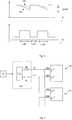
Das Messprinzip dieser Anordnung basiert im Wesentlichen darauf, dass ausgehend von der Phasenverschiebung des emittierten und empfangenen Lichts die Laufzeit des emittierten und reflektierten Lichts ermittelt werden kann. Zu diesem Zwecke werden die Lichtquelle
Dieses Grundprinzip ist schematisch in
In
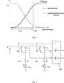
Der mögliche Dynamikbereich erstreckt sich typischerweise über mehrere Größenordnungen. und hängt im Wesentlichen von der Fläche der photosensitiven Schicht der Modulationsgates, Gam, G0, Gbm sowie der Kapazität der Akkumulationsgates Ga, Gb ab. Die Integrationszeit t_int bzw. die Reset-Zeit t_res wird vorzugsweise so festgelegt, dass für den Anwendungsfall der Sensor nicht in die Sättigung gerät. In einer bevorzugten Ausgestaltung wird die Integrationszeit t_int beendet bzw. ein Reset gesetzt, wenn die Gatespannung Ua, Ub an einem Akkumulationsgate Ga, Gb einen Grenzwert überschreitet.The possible dynamic range typically extends over several orders of magnitude. and depends substantially on the area of the photosensitive layer of the modulation gates, Gam, G0, Gbm and the capacitance of the accumulation gates Ga, Gb. The integration time t_int or the reset time t_res is preferably set so that the sensor does not saturate for the application. In a preferred embodiment, the integration time t_int is terminated or a reset is set when the gate voltage Ua, Ub at a storage gate Ga, Gb exceeds a limit value.
Mit abnehmender Lichtmenge bzw. analog mit abnehmender Integrationszeit nimmt jedoch das Potenzial am Akkumulationsgate Ga, Gb immer mehr ab und bewirkt unter anderem aufgrund des abnehmenden Signal/Rausch-Verhältnisses eine zunehmende Unsicherheit bei der Entfernungsbestimmung, so wie es mit der gestrichelten Kurve der Standardabweichung in
Während auf dem tatsächlichen PMD-Chip die photonisch erzeugten Ladungen q durch Anlegen eines Potenzials in Richtung der Akkumulationsgates Ga, Gb abgeleitet werden, ist dieser Vorgang im Ersatzschaltbild als Wechselschalter abgebildet. Auf den ersten Schalter S1 des Wechselschalters wirkt die Modulationsfrequenz MA für den so genannten A-Kanal und auf den zweiten Schalter S2 eine um 180° verschobene Modulationsfrequenz MB für den B-Kanal. Wie bereits in
Auf einer zweiten Anschlussseite sind die Akkumulationskondensatoren Ga, Gb mit einem Versorgungspotenzial V+ verbunden. Die zu den Akkumulationskondensatoren Ga, Gb gelangende Ladung q wird als Spannungssignal Ua, Ub über hochohmige Verstärker von einer Ausleseeinheit
Im dargestellten Beispiel sind die Potentiale so gewählt, dass die Spannung Ua, Ub am Akkumulationskondensator Ga, Gb während der Integrationszeit t_int abnimmt. Die durchgezogene Linie zeigt einen Spannungsverlauf Ua am ersten Akkumulationskondensator Ga und mit gestrichelter Linie ist der Spannungsverlauf Ub für den zweiten Akkumulationskondensator Gb gezeigt. Die Differenz des Spannungssignals ΔUab, ist wie zuvor beschrieben, ein Maß für die Phasenverschiebung bzw. ein Maß für den Objektabstand.In the example shown, the potentials are selected such that the voltage Ua, Ub at the accumulation capacitor Ga, Gb decreases during the integration time t_int. The solid line shows a voltage curve Ua on the first accumulation capacitor Ga, and the dashed line shows the voltage curve Ub for the second accumulation capacitor Gb. The difference of the voltage signal ΔUab, as described above, is a measure of the phase shift or a measure of the object distance.
Je nach Anwendungsfall kann es vorgesehen sein, die Spannungsverlauf Ua, Ub einmalig oder auch mehrfach abzutasten. Bevorzugt wird die Akkumulation der Ladungsträger beendet, bevor das Akkumulationsgate Ga, Gb in Sättigung gerät. In einer bevorzugten Ausführungsform ist es vorgesehen, einen Reset bei einem Überschreiten bzw. Unterschreiten einer bestimmten Spannungsschwelle einzuleiten.Depending on the application, it can be provided to sample the voltage curve Ua, Ub once or even several times. Preferably, the accumulation of the charge carriers is terminated before the accumulation gate Ga, Gb saturates. In a preferred embodiment, it is provided to initiate a reset when a certain voltage threshold is exceeded or undershot.
Im dargestellten Beispiel beaufschlagt ein Modulationstreiber
Es hat sich gezeigt, dass sich die Kapazität bzw. parasitäre Kapazität Cp der photosensitiven Modulationsgates Gam, Gbm in Abhängigkeit der an den Akkumulationsgates Ga, Gb anliegenden Ladung bzw. Spannung verändert. Die sich verändernden Kapazitäten wirken sich insbesondere auf die Phasenlage der Modulationsfrequenz aus. Der Effekt nimmt mit steigender Spannung Ua, Ub an den Akkumulationskondensatoren Ga, Gb zu, und macht sich besonders stark bemerkbar, wenn die Ladung bzw. Spannung Ua, Ub in den Sättigungsbereich gelangt.It has been found that the capacitance or parasitic capacitance Cp of the photosensitive modulation gates Gam, Gbm changes as a function of the charge or voltage applied to the accumulation gates Ga, Gb. The changing capacities have an effect, in particular, on the phase position of the modulation frequency. The effect increases with increasing voltage Ua, Ub to the accumulation capacitors Ga, Gb, and is particularly noticeable when the charge or voltage Ua, Ub reaches the saturation region.
Werden alle Empfangspixel P1, P2 mit ein und derselben Integrationszeit t_int betrieben, besteht die Gefahr, dass die Empfangspixel P1, P2 bzw. die Akkumulationsgates Ga, Gb zu unterschiedlichen Zeiten ihre Sättigung erreichen. Die sich bereits in Sättigung befindlichen Akkumulationsgates, wirken sich jedoch spürbar auf die aufgeprägte Modulationsfrequenz aus, so dass es zu einer leichten Phasenverschiebung des Modulationssignals kommt. Dies führt wiederum dazu, dass die noch messbereiten Modulationsgates Gam, Gbm eine ungenaue Phaseninformation erhalten und hierdurch die Genauigkeit der Entfernungsbestimmung ungünstig beeinflusst wird.If all reception pixels P1, P2 are operated with one and the same integration time t_int, there is a risk that the reception pixels P1, P2 or the accumulation gates Ga, Gb will reach their saturation at different times. However, the already in saturation accumulation gates, however, have a noticeable effect on the impressed modulation frequency, so that there is a slight phase shift of the modulation signal. This in turn means that the modulation gates Gam, Gbm which are still ready to measure receive inaccurate phase information and as a result the accuracy of the distance determination is adversely affected.
Erfindungsgemäß ist es daher vorgesehen auf eine einheitliche Integrationszeit zu verzichten und einen pixelindividuellen Reset durchzuführen. Der Reset ist vorzugsweise so gelegt, dass die maximal an einem Akkumulationsgate Ga, Gb anliegende Spannung Ua, Ub sich nur geringfügig als parasitäre Kapazität der Modulationsgates Gam, Gbm und somit auch auf die Modulationsfrequenz auswirkt. Durch dieses Vorgehen wird unabhängig von dem auf dem einzelnen Pixel auftreffenden Lichtstrom die Modulationsfrequenz für alle Modulationsgates Gam, Gbm phasenkonstant gehalten.According to the invention, it is therefore intended to dispense with a uniform integration time and perform a pixel-individual reset. The reset is preferably set in such a way that the maximum voltage Ua, Ub applied to an accumulation gate Ga, Gb has only a slight effect as a parasitic capacitance of the modulation gates Gam, Gbm and thus also on the modulation frequency. As a result of this procedure, regardless of the luminous flux incident on the individual pixel, the modulation frequency is kept constant in phase for all the modulation gates Gam, Gbm.
BezugszeichenlisteLIST OF REFERENCE NUMBERS
- 1010
- Sendeeinheittransmission unit
- 1212
- BeleuchtungslichtquelleIllumination light source
- 1515
- StrahlformungsoptikBeam shaping optics
- 2020
- Empfangseinheit, TOF-KameraReceiving unit, TOF camera
- 2222
- LichtlaufzeitsensorTransit Time Sensor
- 2525
- Empfangsoptikreceiving optics
- 3030
- Modulatormodulator
- 300300
- Treiberdriver
- 4040
- Objektobject
- 400400
- Ausleseeinheitreadout unit
- 500500
- Bauelementeträgercomponent support
- Gam, G0, GbmGam, G0, Gbm
- ModulationsphotogateModulation photogate
- Ga, GbGa, Gb
- Akkumulationsgate bzw. AkkumulationskondensatorAccumulation gate or accumulation capacitor
- Ladungencharges
- qa, qbqa, qb
- Ladungen am Akkumulationsgate Ga, GbCharges at the accumulation gate Ga, Gb
- Ua, UbUa, Ub
- Spannung am AkkumulationsgateVoltage at the accumulation gate
ZITATE ENTHALTEN IN DER BESCHREIBUNG QUOTES INCLUDE IN THE DESCRIPTION
Diese Liste der vom Anmelder aufgeführten Dokumente wurde automatisiert erzeugt und ist ausschließlich zur besseren Information des Lesers aufgenommen. Die Liste ist nicht Bestandteil der deutschen Patent- bzw. Gebrauchsmusteranmeldung. Das DPMA übernimmt keinerlei Haftung für etwaige Fehler oder Auslassungen.This list of the documents listed by the applicant has been generated automatically and is included solely for the better information of the reader. The list is not part of the German patent or utility model application. The DPMA assumes no liability for any errors or omissions.
Zitierte PatentliteraturCited patent literature
- EP 1777747[0002]EP 1777747[0002]
- US 6587186[0002]US 6587186[0002]
- DE 19704496[0002, 0020]DE 19704496[0002, 0020]
- DE 19704496 C2[0024]DE 19704496 C2[0024]
Claims (4)
Translated fromGermanPriority Applications (1)
| Application Number | Priority Date | Filing Date | Title |
|---|---|---|---|
| DE201010063579DE102010063579A1 (en) | 2010-12-20 | 2010-12-20 | Optical range finder has reset devices that are controlled so as to control discharge of accumulation gates when voltage of accumulation gates reaches or exceeds threshold value |
Applications Claiming Priority (1)
| Application Number | Priority Date | Filing Date | Title |
|---|---|---|---|
| DE201010063579DE102010063579A1 (en) | 2010-12-20 | 2010-12-20 | Optical range finder has reset devices that are controlled so as to control discharge of accumulation gates when voltage of accumulation gates reaches or exceeds threshold value |
Publications (1)
| Publication Number | Publication Date |
|---|---|
| DE102010063579A1true DE102010063579A1 (en) | 2012-06-21 |
Family
ID=46512401
Family Applications (1)
| Application Number | Title | Priority Date | Filing Date |
|---|---|---|---|
| DE201010063579CeasedDE102010063579A1 (en) | 2010-12-20 | 2010-12-20 | Optical range finder has reset devices that are controlled so as to control discharge of accumulation gates when voltage of accumulation gates reaches or exceeds threshold value |
Country Status (1)
| Country | Link |
|---|---|
| DE (1) | DE102010063579A1 (en) |
Cited By (4)
| Publication number | Priority date | Publication date | Assignee | Title |
|---|---|---|---|---|
| DE102016205073B4 (en) | 2015-03-30 | 2021-08-26 | pmdtechnologies ag | Time of flight sensor |
| DE102022110844A1 (en) | 2022-05-03 | 2023-11-09 | Ifm Electronic Gmbh | Method for operating a PMD pixel |
| DE102022110845A1 (en) | 2022-05-03 | 2023-11-09 | Ifm Electronic Gmbh | Method for operating a PMD pixel |
| DE112015003846B4 (en)* | 2014-08-22 | 2024-12-24 | Hamamatsu Photonics K.K. | distance measuring method and distance measuring device |
Citations (3)
| Publication number | Priority date | Publication date | Assignee | Title |
|---|---|---|---|---|
| DE19704496A1 (en) | 1996-09-05 | 1998-03-12 | Rudolf Prof Dr Ing Schwarte | Method and device for determining the phase and / or amplitude information of an electromagnetic wave |
| US6587186B2 (en) | 2000-06-06 | 2003-07-01 | Canesta, Inc. | CMOS-compatible three-dimensional image sensing using reduced peak energy |
| EP1777747A1 (en) | 2005-10-19 | 2007-04-25 | CSEM Centre Suisse d'Electronique et de Microtechnique SA | Device and method for the demodulation of modulated electromagnetic wave fields |
- 2010
- 2010-12-20DEDE201010063579patent/DE102010063579A1/ennot_activeCeased
Patent Citations (4)
| Publication number | Priority date | Publication date | Assignee | Title |
|---|---|---|---|---|
| DE19704496A1 (en) | 1996-09-05 | 1998-03-12 | Rudolf Prof Dr Ing Schwarte | Method and device for determining the phase and / or amplitude information of an electromagnetic wave |
| DE19704496C2 (en) | 1996-09-05 | 2001-02-15 | Rudolf Schwarte | Method and device for determining the phase and / or amplitude information of an electromagnetic wave |
| US6587186B2 (en) | 2000-06-06 | 2003-07-01 | Canesta, Inc. | CMOS-compatible three-dimensional image sensing using reduced peak energy |
| EP1777747A1 (en) | 2005-10-19 | 2007-04-25 | CSEM Centre Suisse d'Electronique et de Microtechnique SA | Device and method for the demodulation of modulated electromagnetic wave fields |
Cited By (6)
| Publication number | Priority date | Publication date | Assignee | Title |
|---|---|---|---|---|
| DE112015003846B4 (en)* | 2014-08-22 | 2024-12-24 | Hamamatsu Photonics K.K. | distance measuring method and distance measuring device |
| DE102016205073B4 (en) | 2015-03-30 | 2021-08-26 | pmdtechnologies ag | Time of flight sensor |
| DE102022110844A1 (en) | 2022-05-03 | 2023-11-09 | Ifm Electronic Gmbh | Method for operating a PMD pixel |
| DE102022110845A1 (en) | 2022-05-03 | 2023-11-09 | Ifm Electronic Gmbh | Method for operating a PMD pixel |
| DE102022110844B4 (en) | 2022-05-03 | 2023-12-28 | Ifm Electronic Gmbh | Method for operating a PMD pixel |
| DE102022110845B4 (en) | 2022-05-03 | 2023-12-28 | Ifm Electronic Gmbh | Method for operating a PMD pixel |
Similar Documents
| Publication | Publication Date | Title |
|---|---|---|
| EP3185038B1 (en) | Optoelectronic sensor and method for measuring a distance | |
| DE102010043768B3 (en) | Time of flight camera | |
| DE102014214733B3 (en) | Light transit time sensor with a device for charge compensation | |
| DE102008018718B4 (en) | Optical distance meter and method for optical distance measurement | |
| WO2014095539A1 (en) | Light propagation time camera with a motion detector | |
| EP1884797B1 (en) | Device and method for determining distance | |
| DE212018000118U1 (en) | LiDAR readout circuit | |
| DE102018120141A1 (en) | Detect light with a variety of avalanche photo diode elements | |
| DE2920951A1 (en) | DISTANCE MEASURING DEVICE | |
| WO2011128131A1 (en) | Distance measuring device having homogenizing measurement evaluation | |
| EP2240797A1 (en) | Optical-electronic distance measuring device | |
| DE102013208802A1 (en) | Time-of-flight (TOF) light sensor of TOF camera for use in three-dimensional-TOF (3D-TOF) camera system, has light transit time pixels that includes different color filters which are distributed in predetermined pattern on sensor area | |
| DE202013105389U1 (en) | Optoelectronic sensor with avalanche photodiode elements operated in Geiger mode | |
| EP3339820B1 (en) | Light receiver and a method for reading out avalanche photodiodes | |
| DE102010063579A1 (en) | Optical range finder has reset devices that are controlled so as to control discharge of accumulation gates when voltage of accumulation gates reaches or exceeds threshold value | |
| DE102013203088B4 (en) | Time of flight camera system | |
| DE102014207163A1 (en) | Time of flight camera system | |
| DE102012223298A1 (en) | Light running time sensor e.g. photo mixture detector camera system, has light running time pixel and reference light running time pixel for reception of modulated reference light, where reference pixel exhibits nonlinear curve | |
| DE102016213217A1 (en) | Time of flight camera system | |
| DE102016219170A1 (en) | Time of flight camera system | |
| DE102011089642B4 (en) | time-of-flight sensor | |
| DE102018132473A1 (en) | Optoelectronic sensor and method for detecting an object | |
| WO2022048862A1 (en) | Optical surround sensor with compensation of the ambient light | |
| DE102013208805B4 (en) | Light transit time sensor with buffer | |
| DE102018131584B4 (en) | Method for measuring distance using a time-of-flight distance measuring system and corresponding time-of-flight distance measuring system |
Legal Events
| Date | Code | Title | Description |
|---|---|---|---|
| R016 | Response to examination communication | ||
| R016 | Response to examination communication | ||
| R081 | Change of applicant/patentee | Owner name:PMDTECHNOLOGIES AG, DE Free format text:FORMER OWNER: IFM ELECTRONIC GMBH, 45128 ESSEN, DE | |
| R016 | Response to examination communication | ||
| R002 | Refusal decision in examination/registration proceedings | ||
| R003 | Refusal decision now final |