DE102010047128A1 - Hall sensor arrangement for redundantly measuring a magnetic field - Google Patents
Hall sensor arrangement for redundantly measuring a magnetic fieldDownload PDFInfo
- Publication number
- DE102010047128A1 DE102010047128A1DE201010047128DE102010047128ADE102010047128A1DE 102010047128 A1DE102010047128 A1DE 102010047128A1DE 201010047128DE201010047128DE 201010047128DE 102010047128 ADE102010047128 ADE 102010047128ADE 102010047128 A1DE102010047128 A1DE 102010047128A1
- Authority
- DE
- Germany
- Prior art keywords
- hall sensor
- magnetic field
- semiconductor substrate
- sensor arrangement
- hall
- Prior art date
- Legal status (The legal status is an assumption and is not a legal conclusion. Google has not performed a legal analysis and makes no representation as to the accuracy of the status listed.)
- Withdrawn
Links
- 239000004065semiconductorSubstances0.000claimsabstractdescription39
- 239000000758substrateSubstances0.000claimsabstractdescription36
- 150000001875compoundsChemical class0.000claimsdescription5
- 238000000465mouldingMethods0.000claimsdescription5
- 239000000853adhesiveSubstances0.000claimsdescription2
- 230000001070adhesive effectEffects0.000claimsdescription2
- 238000005259measurementMethods0.000abstractdescription2
- 238000002161passivationMethods0.000description7
- 230000005355Hall effectEffects0.000description2
- 230000000712assemblyEffects0.000description2
- 238000000429assemblyMethods0.000description2
- 238000005452bendingMethods0.000description2
- 239000004020conductorSubstances0.000description2
- 230000009977dual effectEffects0.000description2
- 238000000034methodMethods0.000description2
- 230000008092positive effectEffects0.000description2
- 238000010008shearingMethods0.000description2
- 239000000126substanceSubstances0.000description2
- BUHVIAUBTBOHAG-FOYDDCNASA-N(2r,3r,4s,5r)-2-[6-[[2-(3,5-dimethoxyphenyl)-2-(2-methylphenyl)ethyl]amino]purin-9-yl]-5-(hydroxymethyl)oxolane-3,4-diolChemical compoundCOC1=CC(OC)=CC(C(CNC=2C=3N=CN(C=3N=CN=2)[C@H]2[C@@H]([C@H](O)[C@@H](CO)O2)O)C=2C(=CC=CC=2)C)=C1BUHVIAUBTBOHAG-FOYDDCNASA-N0.000description1
- 230000002411adverseEffects0.000description1
- 230000006378damageEffects0.000description1
- 230000000694effectsEffects0.000description1
- 238000005516engineering processMethods0.000description1
- 238000009434installationMethods0.000description1
- 150000004767nitridesChemical class0.000description1
- 238000005476solderingMethods0.000description1
- 230000000930thermomechanical effectEffects0.000description1
Images

Classifications
- G—PHYSICS
- G01—MEASURING; TESTING
- G01R—MEASURING ELECTRIC VARIABLES; MEASURING MAGNETIC VARIABLES
- G01R33/00—Arrangements or instruments for measuring magnetic variables
- G01R33/02—Measuring direction or magnitude of magnetic fields or magnetic flux
- G01R33/06—Measuring direction or magnitude of magnetic fields or magnetic flux using galvano-magnetic devices
- G01R33/07—Hall effect devices
- G—PHYSICS
- G01—MEASURING; TESTING
- G01R—MEASURING ELECTRIC VARIABLES; MEASURING MAGNETIC VARIABLES
- G01R33/00—Arrangements or instruments for measuring magnetic variables
- G01R33/02—Measuring direction or magnitude of magnetic fields or magnetic flux
- G01R33/06—Measuring direction or magnitude of magnetic fields or magnetic flux using galvano-magnetic devices
- G01R33/09—Magnetoresistive devices
- G01R33/093—Magnetoresistive devices using multilayer structures, e.g. giant magnetoresistance sensors
- A—HUMAN NECESSITIES
- A61—MEDICAL OR VETERINARY SCIENCE; HYGIENE
- A61B—DIAGNOSIS; SURGERY; IDENTIFICATION
- A61B90/00—Instruments, implements or accessories specially adapted for surgery or diagnosis and not covered by any of the groups A61B1/00 - A61B50/00, e.g. for luxation treatment or for protecting wound edges
- A61B90/08—Accessories or related features not otherwise provided for
- A61B2090/0818—Redundant systems, e.g. using two independent measuring systems and comparing the signals
- H—ELECTRICITY
- H01—ELECTRIC ELEMENTS
- H01L—SEMICONDUCTOR DEVICES NOT COVERED BY CLASS H10
- H01L2224/00—Indexing scheme for arrangements for connecting or disconnecting semiconductor or solid-state bodies and methods related thereto as covered by H01L24/00
- H01L2224/01—Means for bonding being attached to, or being formed on, the surface to be connected, e.g. chip-to-package, die-attach, "first-level" interconnects; Manufacturing methods related thereto
- H01L2224/42—Wire connectors; Manufacturing methods related thereto
- H01L2224/47—Structure, shape, material or disposition of the wire connectors after the connecting process
- H01L2224/48—Structure, shape, material or disposition of the wire connectors after the connecting process of an individual wire connector
- H01L2224/4805—Shape
- H01L2224/4809—Loop shape
- H01L2224/48091—Arched
- H—ELECTRICITY
- H01—ELECTRIC ELEMENTS
- H01L—SEMICONDUCTOR DEVICES NOT COVERED BY CLASS H10
- H01L2224/00—Indexing scheme for arrangements for connecting or disconnecting semiconductor or solid-state bodies and methods related thereto as covered by H01L24/00
- H01L2224/01—Means for bonding being attached to, or being formed on, the surface to be connected, e.g. chip-to-package, die-attach, "first-level" interconnects; Manufacturing methods related thereto
- H01L2224/42—Wire connectors; Manufacturing methods related thereto
- H01L2224/47—Structure, shape, material or disposition of the wire connectors after the connecting process
- H01L2224/48—Structure, shape, material or disposition of the wire connectors after the connecting process of an individual wire connector
- H01L2224/481—Disposition
- H01L2224/48151—Connecting between a semiconductor or solid-state body and an item not being a semiconductor or solid-state body, e.g. chip-to-substrate, chip-to-passive
- H01L2224/48221—Connecting between a semiconductor or solid-state body and an item not being a semiconductor or solid-state body, e.g. chip-to-substrate, chip-to-passive the body and the item being stacked
- H01L2224/48245—Connecting between a semiconductor or solid-state body and an item not being a semiconductor or solid-state body, e.g. chip-to-substrate, chip-to-passive the body and the item being stacked the item being metallic
- H01L2224/48247—Connecting between a semiconductor or solid-state body and an item not being a semiconductor or solid-state body, e.g. chip-to-substrate, chip-to-passive the body and the item being stacked the item being metallic connecting the wire to a bond pad of the item
Landscapes
- Physics & Mathematics (AREA)
- Condensed Matter Physics & Semiconductors (AREA)
- General Physics & Mathematics (AREA)
- Hall/Mr Elements (AREA)
- Measuring Magnetic Variables (AREA)
Abstract
Translated fromGermanDescription
Translated fromGermanDie vorliegende Erfindung betrifft eine Hallsensoranordnung zum redundanten Messen eines Magnetfeldes.The present invention relates to a Hall sensor arrangement for redundantly measuring a magnetic field.
Magnetfeldsensoren haben ein weites Einsatzgebiet. Magnetfeldsensoren werden in Kombination mit Magnetfelderzeugern, wie einfachen Magneten, oft dazu verwendet Positionen von mechanischen Komponenten zu bestimmen. Im Automobil werden Magnetfeldsensoren oft dazu verwendet, Positionen rotatorischer Komponenten, wie Wellen oder translatorischer Komponenten, wie Ventilen zu bestimmen. Hallsensoren zeichnen sich, im Vergleich zu GMR-Sensoren, dadurch aus, dass Hallsensoren die Magnetfeldkomponente messen, die senkrecht zum Hallsensor ist.Magnetic field sensors have a wide field of application. Magnetic field sensors, in combination with magnetic field generators, such as simple magnets, are often used to determine positions of mechanical components. In automobiles, magnetic field sensors are often used to determine positions of rotational components, such as shafts or translatory components, such as valves. Hall sensors are characterized, in comparison to GMR sensors, in that Hall sensors measure the magnetic field component which is perpendicular to the Hall sensor.
Ein Einsatz in sicherheitsrelevanten Anwendungen erfordert eine höchste Betriebssicherheit der eingesetzten Komponenten, also auch eine höchste Betriebsicherheit bei Magnetfeldsensoren. Als Beispiel für die Anforderungen an sicherheitsrelevante Systeme, beziehungsweise Komponenten, sei die
Takehashi et al. zeigt in
Strack et al. zeigt in
Außerlechner zeigt in
Das
Der Einsatz von Magnetfeldsensoren in einem sicherheitsrelevanten Bereich, wie beispielsweise im Automobil, erfordert den Verzicht auf Komponenten, die Lebensdauer eines Magnetfeldsensors negativ beeinflussen können, wie beispielsweise feuchtigkeitssensitive Substanzen in einen Halbleitergehäuse.The use of magnetic field sensors in a safety-relevant area, such as in the automobile, requires the abandonment of components that can adversely affect the life of a magnetic field sensor, such as moisture-sensitive substances in a semiconductor package.
Der Einsatz von Magnetfeldsensoren in einem sicherheitsrelevanten Bereich, wie beispielsweise im Automobil, erfordert zudem redundante bzw. teilweise redundante Systeme.The use of magnetic field sensors in a safety-relevant area, such as in the automobile, also requires redundant or partially redundant systems.
Trotz der hohen Anforderungen an Sicherheit, Zuverlässigkeit und Redundanz müssen Magnetfeldsensoren, insbesondere im Automobil, preisgünstig sein.Despite the high demands on safety, reliability and redundancy, magnetic field sensors, especially in the automobile, must be inexpensive.
Der vorliegenden Erfindung liegt daher die Aufgabe zugrunde, einen Magnetfeldsensor bereitzustellen, der redundant, zuverlässig, sicher und preisgünstig ist.The present invention is therefore based on the object to provide a magnetic field sensor that is redundant, reliable, secure and inexpensive.
Diese Aufgabe wird durch eine Hallsensoranordnung mit den Merkmalen des Anspruchs 1 gelöst.This object is achieved by a Hall sensor arrangement with the features of claim 1.
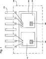
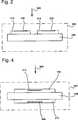
Eine Hallsensoranordnung zum redundanten Messen eines Magnetfeldes weist einen ersten Hallsensor auf einer Oberseite eines ersten Halbleitersubstrats, einen zweiten Hallsensor auf einer Oberseite eines zweiten Halbleitersubstrats und einen Träger mit einer Oberseite und einer Unterseite auf. Der erste Hallsensor ist auf der Oberseite des Trägers angeordnet, der zweite Hallsensor ist auf der Unterseite des Trägers angeordnet. Die Hallsensoren sind derart angeordnet, dass die senkrecht auf den Träger projezierte messende Fläche des ersten Hallsensors sich zumindest teilweise mit der senkrecht auf den Träger projezierten messenden Fläche des zweiten Hallsensors überlappt.A Hall sensor arrangement for redundantly measuring a magnetic field has a first Hall sensor on an upper side of a first semiconductor substrate, a second Hall sensor on an upper side of a second semiconductor substrate and a carrier with an upper side and a lower side. The first Hall sensor is arranged on the upper side of the carrier, the second Hall sensor is arranged on the underside of the carrier. The Hall sensors are arranged such that the measuring surface of the first Hall sensor projected perpendicularly onto the carrier overlaps at least partially with the measuring surface of the second Hall sensor projected perpendicular to the carrier.
Die Hallsensoren sind somit derart angeordnet dass die Hallsensoren dieselben Magnetfeldlinien eines von außen angelegten Magnetfeldes messen. Hallsensoren messen den senkrechten Anteil der Magnetfeldlinien, die die Hallsensoren durchdringen. Die Hallsensoranordnung bewirkt, dass die Hallsensoren nahezu dasselbe magnetische Feld messen, so dass die Messergebnisse der beiden Hallsensoren nahezu redundant zueinander sind. Je nachdem, wie weit sich die die senkrecht auf den Träger projezierten messenden Flächen des ersten Hallsensors und des zweiten Hallsensors überlappen, liegt eine teilweise oder vollständige Redundanz vor.The Hall sensors are thus arranged such that the Hall sensors measure the same magnetic field lines of an externally applied magnetic field. Hall sensors measure the vertical part of the magnetic field lines that penetrate the Hall sensors. The Hall sensor arrangement causes the Hall sensors to measure almost the same magnetic field, so that the measurement results of the two Hall sensors are almost redundant to each other. Depending on how far overlap the perpendicular projecting onto the support measuring surfaces of the first Hall sensor and the second Hall sensor, there is a partial or complete redundancy.
Ein Vorteil von Hallsensoren ist, dass Hallsensoren ohne großen Aufwand mit einer bestehenden Halbleitertechnologie gefertigt werden können, so dass es möglich ist einen Hallsensor mit einer komplexen integierten Schaltung in einem Halbleitersubstrat zu integrieren. Ein GMR-Sensor wird im Gegensatz dazu auf einer integrierten Schaltung aufgebracht, nachdem diese durch geeignete Mittel passiviert wurde. Der GMR-Sensor an sich muss durch weitere geeignete Mittel passiviert werden. Diese Passivierungsschichten haben den Nachteil, dass diese empfindlicher auf Feuchtigkeit reagieren als die abschließende Passivierung des Halbleitersubstarts.An advantage of Hall sensors is that Hall sensors can be manufactured with little effort with an existing semiconductor technology, so that it is possible to integrate a Hall sensor with a complex integrated circuit in a semiconductor substrate. In contrast, a GMR sensor is integrated into an integrated circuit applied after it has been passivated by suitable means. The GMR sensor itself must be passivated by other suitable means. These passivation layers have the disadvantage that they are more sensitive to moisture than the final passivation of the semiconductor sub-start.
Die erfindungsgemäße Hallsensoranordnung hat den weiteren Vorteil, dass die Hallsensoren mit ihren zumindest teilweise überlappenden Hallsensoren dieselben Magnetfeldanteile eines außerhalb angelegten Magnetfeldes messen, da ein von außen angelegtes Magnetfeld beide Hallsensoren gleichermaßen durchströmt. Die Hallsensoranordnung hat daher den Vorteil, dass eine vollständige Redundanz der Hallsensoren erreicht werden kann. Die Hallsensoranordnung weist den Vorteil auf, dass das Gehäuse zur Aufnahme der Hallsensoranordnung klein und kompakt ist. Ein kleines Gehäuse erweitert die Verwendbarkeit, mit Hinblick auf die zunehmende Miniaturisierung von elektronischen Platinen und Baugruppen, stark. Ein kleines Gehäuse ist, allein durch seine Größe, kleinen mechanischen Belastungen, wie Scher- und Biegekräften, ausgesetzt, was die Zuverlässigkeit einer solchen Hallsensoranordnung erhöht.The Hall sensor arrangement according to the invention has the further advantage that the Hall sensors with their at least partially overlapping Hall sensors measure the same magnetic field components of a magnetic field applied externally, since an externally applied magnetic field flows through both Hall sensors equally. The Hall sensor arrangement therefore has the advantage that complete redundancy of the Hall sensors can be achieved. The Hall sensor arrangement has the advantage that the housing for receiving the Hall sensor arrangement is small and compact. A small package greatly expands the usability in view of the increasing miniaturization of electronic boards and assemblies. A small housing, by its size alone, is subject to small mechanical stresses, such as shearing and bending forces, which increases the reliability of such a Hall sensor arrangement.
Ein weiterer Vorteil der Hallsensoranordnung besteht darin, dass zwischen den beiden Hallsensoren keine Folie aufgebracht werden muss, da beide Hallsensoren fest auf einem Substrat aufgebracht werden können. Durch den Verzicht auf Montagehilfen, ergibt sich ein flaches und in der Gesamtheit ausgewogenes Gehäuse.Another advantage of the Hall sensor arrangement is that no film must be applied between the two Hall sensors, since both Hall sensors can be firmly applied to a substrate. By dispensing with assembly aids, results in a flat and balanced in the overall housing.
Feuchtigkeitsensive Substanzen, wie beispielsweise Die-Attach-Folien, Poly-Immide als Passivierungsschichten können die Zerstörung eines Gehäuses begünstigen. Durch den Verzicht auf solche beispielhaften Montagehilfen ergibt sich als weiterer Vorteil, dass die Hallsensoranordnung unempfindlich gegenüber Feuchtigkeit ist, da es nur keine Gehäusebestandteile gibt, die Feuchtigkeit aufnehmen oder empfindlich gegenüber Feuchtigkeit sind. Durch diesen Verzicht bleibt das Gehäuse der Hallsensoranordnung klein und kompakt. Ein weiterer Vorteil der Hallsensoranordnung ergibt sich daraus, dass zur elektrischen Verbindung des oberen Hallsensors mit den Kontakten des Gehäuses nur kurze Bonddrähte nötig sind. Ein weiterer Vorteil einer erfindungsgemäßen Hallsensoranordnung ist, dass ein diese Hallsensoranordnung sehr gut ausbalanciert und nicht unwuchtig ist, was sich positiv auf das thermomechanische Verhalten auswirkt und damit auch positiv auf die Zuverlässigkeit auswirkt.Moisture-imparting substances, such as die-attach films, poly-Immide as passivation layers can promote the destruction of a housing. By dispensing with such exemplary mounting aids, it is a further advantage that the Hall sensor assembly is insensitive to moisture, since there are only no housing components that absorb moisture or are sensitive to moisture. Through this waiver, the housing of the Hall sensor assembly remains small and compact. Another advantage of the Hall sensor arrangement results from the fact that only short bonding wires are necessary for electrical connection of the upper Hall sensor with the contacts of the housing. Another advantage of a Hall sensor arrangement according to the invention is that this Hall sensor arrangement is very well balanced and not unbalanced, which has a positive effect on the thermo-mechanical behavior and thus also has a positive effect on the reliability.
Bei einem Ausführungsbeispiel der Hallsensoranordnung zum redundanten Messen eines Magnetfeldes können die Hallsensoren von einer Pressmasse vollständig umschlossen sein. Als besonderer Vorteil ergibt sich, dass neben der standardmäßigen Passivierung der Hallsensoren, z. B. Oxid-, Nitrid-, Immid-Passivierungen auf dem Halbleitersubstrat verwendeten Passivierungen, keine weiteren Passivierungen verwendet werden müssen. Als weiterer besonderer Vorteil ergibt sich, dass neben einer standardmäßigen Pressmasse, weder eine besondere Pressmasse noch ein besonderes Verfahren zur Umschließung der Hallsensoranordnung verwendet werden muss.In one embodiment of the Hall sensor arrangement for redundantly measuring a magnetic field, the Hall sensors may be completely enclosed by a molding compound. A particular advantage is that in addition to the standard passivation of the Hall sensors, z. As oxide, nitride, Immid passivations used on the semiconductor substrate passivation, no further passivation must be used. Another particular advantage is that in addition to a standard molding compound, neither a special molding compound nor a special method for enclosing the Hall sensor assembly must be used.
Gemäß einem weiteren Ausführungsbeispiel können das erste und das zweite Halbleitersubstrat der Hallsensoranordnung zum redundanten Messen eines Magnetfeldes eine integrierte Schaltung aufweisen.According to a further embodiment, the first and the second semiconductor substrate of the Hall sensor arrangement for redundantly measuring a magnetic field may comprise an integrated circuit.
Das erste und das zweite Halbleitersubstrat der Hallsensoranordnung zum redundanten Messen eines Magnetfeldes können gegeneinander verdreht angeordnet sein.The first and the second semiconductor substrate of the Hall sensor arrangement for redundantly measuring a magnetic field can be arranged rotated relative to one another.
Die Halbleitersubstrate der Hallsensoranordnung zum redundanten Messen eines Magnetfeldes weisen eine der Oberseite gegenüberliegende Unterseite auf, wobei Halbleitersubstrate mit ihren Unterseiten auf dem Träger angeordnet sein können.The semiconductor substrates of the Hall sensor arrangement for redundantly measuring a magnetic field have an underside which is opposite the top side, wherein semiconductor substrates may be arranged with their undersides on the carrier.
Die Unterseiten der Halbleitersubstrate der Hallsensoranordnung zum redundanten Messen eines Magnetfeldes können mit einem isolierenden Kleber auf dem Träger befestigt sein.The bottoms of the semiconductor substrates of the Hall sensor assembly for redundantly measuring a magnetic field may be secured to the carrier with an insulating adhesive.
Die Hallsensoranordnung kann Kontaktstreifen aufweisen und die Hallsensoren können elektrische Kontakte zum Bereitstellen eines Hallsignals aufweisen. Die elektrischen Kontakte des ersten und des zweiten Hallsensors sind an eigene Kontaktstreifen angeschlossen. Durch diese Anordnung können die Hallsensoren unabhängig voneinander angeschlossen werden, so dass auch die Messwerte der Hallsensoren unabhängig voneinander ausgelesen werden können. Die Hallsensoren können also redundant ausgelesen werden. Eine integrierte Schaltung kann die Betriebsparameter der Hallsensoren einstellen. Das erste Halbleitersubstrat kann lediglich einen Hallsensor aufweisen, während das zweite Halbleitersubstrat eine integrierte Schaltung zur Ansteuerung des ersten und des zweiten Hallsensors aufweist.The Hall sensor arrangement may have contact strips and the Hall sensors may have electrical contacts for providing a Hall signal. The electrical contacts of the first and the second Hall sensor are connected to separate contact strips. By this arrangement, the Hall sensors can be connected independently of each other, so that the measured values of the Hall sensors can be read independently. The Hall sensors can therefore be read redundantly. An integrated circuit can adjust the operating parameters of the Hall sensors. The first semiconductor substrate may have only one Hall sensor, while the second semiconductor substrate has an integrated circuit for driving the first and the second Hall sensor.
Die Halbleitersubstrate können elektrische Kontakte zum Bereitstellen elektrischer Signale aufweisen, wobei die elektrischen Kontakte des ersten und des zweiten Halbleitersubstrats an eigene Kontaktstreifen angeschlossen sind. Durch diese Anordnung können nicht nur die Hallsensoren, sondern auch die integrierten Schaltungen unabhängig voneinander angeschlossen werden, so dass sowohl die Messwerte der Hallsensoren als die Einstellungen der Hallsensoren unabhängig voneinander ausgelesen und eingestellte werden können. Die Halbleitersubstrate mit den Hallsensoren und den integrierten Schaltungen können identisch sein. Durch diese Anordnung wird eine vollständige Redundanz erreicht.The semiconductor substrates may have electrical contacts for providing electrical signals, wherein the electrical contacts of the first and the second semiconductor substrate are connected to separate contact strips. By this arrangement, not only the Hall sensors, but also the integrated circuits can be connected independently of each other, so that both the measured values of the Hall sensors and the settings of the Hall sensors independently can be read out and set. The semiconductor substrates with the Hall sensors and the integrated circuits may be identical. By this arrangement, a complete redundancy is achieved.
Die Kontaktstreifen zur elektrischen Verbindung des ersten und des zweiten Halbleitersubstrats sind auf gegenüberliegenden Seiten des Trägers angeordnet. Dadurch entsteht eine symmetrische Kontaktieranordnung und die Abmessungen des Gehäuses sind etwas kleiner als bei einer einseitigen Herausführung der Kontaktstreifen. Außerdem entsteht so ein echtes SMD konformes Bauteil. Die Anordnung aller Kontakte auf einer Seite kann beim Auflöten eines Bauteiles dazu führen, das sich der Gehäusekörper aufstellt (Tombstone Effekt), was bei der niedrigen Einbauhöhe zu Problemen beim Kunden führen kann.The contact strips for electrical connection of the first and the second semiconductor substrate are arranged on opposite sides of the carrier. This results in a symmetrical contacting arrangement and the dimensions of the housing are slightly smaller than in a one-sided lead-out of the contact strip. In addition, this creates a true SMD compliant component. The arrangement of all contacts on one side can lead to the soldering of a component, which sets up the housing body (tombstone effect), which can lead to problems at the customer with the low installation height.
Ausführungsformen werden nachfolgend unter Bezugnahme auf die folgenden Zeichnungen näher erläutert, in denenEmbodiments are explained in more detail below with reference to the following drawings in which
Zur elektrischen Verbindung sind Kontaktstreifen
ZITATE ENTHALTEN IN DER BESCHREIBUNG QUOTES INCLUDE IN THE DESCRIPTION
Diese Liste der vom Anmelder aufgeführten Dokumente wurde automatisiert erzeugt und ist ausschließlich zur besseren Information des Lesers aufgenommen. Die Liste ist nicht Bestandteil der deutschen Patent- bzw. Gebrauchsmusteranmeldung. Das DPMA übernimmt keinerlei Haftung für etwaige Fehler oder Auslassungen.This list of the documents listed by the applicant has been generated automatically and is included solely for the better information of the reader. The list is not part of the German patent or utility model application. The DPMA assumes no liability for any errors or omissions.
Zitierte PatentliteraturCited patent literature
- US 5783463[0004]US 5783463[0004]
- DE 19815906[0005]DE 19815906[0005]
- DE 10315532[0006]DE 10315532[0006]
Zitierte Nicht-PatentliteraturCited non-patent literature
- IEC 61508[0003]IEC 61508[0003]
- Datenblatt des MLX90277 von Melexis beschreibt einen „Dual Programmable Linear Hall Effect Sensor”[0007]Melexis MLX90277 Datasheet Describes "Dual Programmable Linear Hall Effect Sensor"[0007]
Claims (10)
Translated fromGermanPriority Applications (4)
| Application Number | Priority Date | Filing Date | Title |
|---|---|---|---|
| DE201010047128DE102010047128A1 (en) | 2010-09-30 | 2010-09-30 | Hall sensor arrangement for redundantly measuring a magnetic field |
| US13/249,301US9151809B2 (en) | 2010-09-30 | 2011-09-30 | Hall sensor arrangement for the redundant measurement of a magnetic field |
| US14/831,898US9678174B2 (en) | 2010-09-30 | 2015-08-21 | Method for redundantly measuring a magnetic field |
| US15/472,343US10324143B2 (en) | 2010-09-30 | 2017-03-29 | Apparatus for redundantly measuring a magnetic field |
Applications Claiming Priority (1)
| Application Number | Priority Date | Filing Date | Title |
|---|---|---|---|
| DE201010047128DE102010047128A1 (en) | 2010-09-30 | 2010-09-30 | Hall sensor arrangement for redundantly measuring a magnetic field |
Publications (1)
| Publication Number | Publication Date |
|---|---|
| DE102010047128A1true DE102010047128A1 (en) | 2012-04-05 |
Family
ID=45832508
Family Applications (1)
| Application Number | Title | Priority Date | Filing Date |
|---|---|---|---|
| DE201010047128WithdrawnDE102010047128A1 (en) | 2010-09-30 | 2010-09-30 | Hall sensor arrangement for redundantly measuring a magnetic field |
Country Status (2)
| Country | Link |
|---|---|
| US (3) | US9151809B2 (en) |
| DE (1) | DE102010047128A1 (en) |
Cited By (5)
| Publication number | Priority date | Publication date | Assignee | Title |
|---|---|---|---|---|
| WO2016128175A3 (en)* | 2015-02-10 | 2016-10-13 | Robert Bosch Gmbh | Sensor housing for a wheel sensor device, wheel sensor device und connecting component thereof |
| WO2017178215A1 (en)* | 2016-04-15 | 2017-10-19 | Continental Teves Ag & Co. Ohg | Wheel rotational-speed sensor and fastening system for assembling a wheel rotational-speed sensor |
| WO2017178216A1 (en)* | 2016-04-15 | 2017-10-19 | Continental Teves Ag & Co. Ohg | Wheel speed sensor |
| CN107402094A (en)* | 2016-05-19 | 2017-11-28 | 株式会社捷太格特 | Sensor unit, collection magnetic module and sensor device |
| CN113608152A (en)* | 2016-12-16 | 2021-11-05 | 迈来芯电子科技有限公司 | Magnetic sensor |
Families Citing this family (9)
| Publication number | Priority date | Publication date | Assignee | Title |
|---|---|---|---|---|
| DE202014103355U1 (en)* | 2014-07-22 | 2014-08-19 | Infineon Technologies Ag | An apparatus and a system for detecting a physical quantity |
| DE102014016565B3 (en)* | 2014-11-11 | 2015-11-12 | Micronas Gmbh | Circuit case |
| JPWO2018012272A1 (en) | 2016-07-12 | 2019-05-09 | パナソニックIpマネジメント株式会社 | Magnetic sensor and detection device using the same |
| DE102017124542B4 (en) | 2017-10-20 | 2023-12-21 | Infineon Technologies Ag | MAGNETIC FIELD SENSOR ARRANGEMENT AND METHOD FOR MEASURING AN EXTERNAL MAGNETIC FIELD |
| JP6809442B2 (en)* | 2017-11-27 | 2021-01-06 | Tdk株式会社 | How to implement the sensor system, sensor module and sensor system |
| US11112273B2 (en) | 2018-10-25 | 2021-09-07 | KSR IP Holdings, LLC | Two magnet sensor systems |
| JP2021064780A (en) | 2019-10-11 | 2021-04-22 | メレキシス テクノロジーズ エス エーMelexis Technologies SA | Laminate die assembly |
| DE102021120054A1 (en) | 2021-08-02 | 2023-02-02 | Infineon Technologies Ag | SENSOR CHIP WITH A NUMBER OF INTEGRATED SENSOR CIRCUITS |
| CN113759295B (en)* | 2021-08-06 | 2024-11-01 | 苏州矩阵光电有限公司 | Integrated Hall magnetic sensor and manufacturing method thereof |
Citations (6)
| Publication number | Priority date | Publication date | Assignee | Title |
|---|---|---|---|---|
| US5783463A (en) | 1994-04-15 | 1998-07-21 | Matsushita Electric Industrial Co., Ltd. | Semiconductor device and method of producing said semiconductor device |
| DE19815906A1 (en) | 1998-04-08 | 1999-10-14 | Siemens Ag | Encapsulated power semiconductor device |
| EP1382935A1 (en)* | 2002-07-19 | 2004-01-21 | Fernsteuergeräte Kurt Oelsch GmbH | Redundant angular transducer having two magnetoresistive sensor elements |
| DE10315532A1 (en) | 2003-04-04 | 2004-11-11 | Infineon Technologies Ag | Current sensing integrated circuit has two magnetic field sensor chips arranged on opposing sides of framework and an evaluation unit all contained within sensor housing |
| DE102005060713A1 (en)* | 2005-12-19 | 2007-06-21 | Austriamicrosystems Ag | Magnetic field sensor arrangement and method for non-contact measurement of a magnetic field |
| DE102006032277A1 (en)* | 2006-07-12 | 2008-01-17 | Infineon Technologies Ag | Magnetic field sensor device |
Family Cites Families (16)
| Publication number | Priority date | Publication date | Assignee | Title |
|---|---|---|---|---|
| JPH02192781A (en)* | 1989-01-20 | 1990-07-30 | Mitsubishi Electric Corp | Hall element and magnetic sensor system |
| KR930010072B1 (en)* | 1990-10-13 | 1993-10-14 | 금성일렉트론 주식회사 | CCD package and manufacturing method |
| DE19817356A1 (en)* | 1998-04-18 | 1999-10-21 | Bosch Gmbh Robert | Angle indicator for determining an angle between a sensor arrangement and a magnetic field |
| JP3522177B2 (en)* | 2000-02-21 | 2004-04-26 | 株式会社三井ハイテック | Method for manufacturing semiconductor device |
| DE20018538U1 (en)* | 2000-10-27 | 2002-03-07 | Mannesmann Vdo Ag | sensor module |
| JP4637380B2 (en)* | 2001-02-08 | 2011-02-23 | ルネサスエレクトロニクス株式会社 | Semiconductor device |
| DE60229675D1 (en)* | 2001-11-09 | 2008-12-11 | Wispry Inc | Three-layer beam MEMS device and related methods |
| US6777926B2 (en)* | 2002-08-02 | 2004-08-17 | Honeywell International Inc. | Phase stability of non-sinusoidal signals utilizing two differential halls |
| US20070040803A1 (en)* | 2005-08-17 | 2007-02-22 | Sauer-Danfoss Inc. | Method of joining a sintered magnet to a pivot arm |
| JP4998268B2 (en)* | 2005-08-24 | 2012-08-15 | 富士通セミコンダクター株式会社 | Semiconductor device and manufacturing method thereof |
| US7116101B1 (en)* | 2005-12-20 | 2006-10-03 | Honeywell International Inc. | Specific location of hall chips for sensing redundant angular positions |
| US7768083B2 (en)* | 2006-01-20 | 2010-08-03 | Allegro Microsystems, Inc. | Arrangements for an integrated sensor |
| DE102006046984A1 (en)* | 2006-10-04 | 2008-04-10 | Siemens Ag | Method for producing a carrier element with an angle sensor |
| US8093670B2 (en)* | 2008-07-24 | 2012-01-10 | Allegro Microsystems, Inc. | Methods and apparatus for integrated circuit having on chip capacitor with eddy current reductions |
| DE102012212367A1 (en)* | 2011-07-14 | 2013-01-17 | Continental Teves Ag & Co. Ohg | Device for measuring an electric current |
| DE202014103355U1 (en)* | 2014-07-22 | 2014-08-19 | Infineon Technologies Ag | An apparatus and a system for detecting a physical quantity |
- 2010
- 2010-09-30DEDE201010047128patent/DE102010047128A1/ennot_activeWithdrawn
- 2011
- 2011-09-30USUS13/249,301patent/US9151809B2/enactiveActive
- 2015
- 2015-08-21USUS14/831,898patent/US9678174B2/enactiveActive
- 2017
- 2017-03-29USUS15/472,343patent/US10324143B2/enactiveActive
Patent Citations (6)
| Publication number | Priority date | Publication date | Assignee | Title |
|---|---|---|---|---|
| US5783463A (en) | 1994-04-15 | 1998-07-21 | Matsushita Electric Industrial Co., Ltd. | Semiconductor device and method of producing said semiconductor device |
| DE19815906A1 (en) | 1998-04-08 | 1999-10-14 | Siemens Ag | Encapsulated power semiconductor device |
| EP1382935A1 (en)* | 2002-07-19 | 2004-01-21 | Fernsteuergeräte Kurt Oelsch GmbH | Redundant angular transducer having two magnetoresistive sensor elements |
| DE10315532A1 (en) | 2003-04-04 | 2004-11-11 | Infineon Technologies Ag | Current sensing integrated circuit has two magnetic field sensor chips arranged on opposing sides of framework and an evaluation unit all contained within sensor housing |
| DE102005060713A1 (en)* | 2005-12-19 | 2007-06-21 | Austriamicrosystems Ag | Magnetic field sensor arrangement and method for non-contact measurement of a magnetic field |
| DE102006032277A1 (en)* | 2006-07-12 | 2008-01-17 | Infineon Technologies Ag | Magnetic field sensor device |
Non-Patent Citations (2)
| Title |
|---|
| Datenblatt des MLX90277 von Melexis beschreibt einen "Dual Programmable Linear Hall Effect Sensor" |
| IEC 61508 |
Cited By (9)
| Publication number | Priority date | Publication date | Assignee | Title |
|---|---|---|---|---|
| WO2016128175A3 (en)* | 2015-02-10 | 2016-10-13 | Robert Bosch Gmbh | Sensor housing for a wheel sensor device, wheel sensor device und connecting component thereof |
| US10509050B2 (en) | 2015-02-10 | 2019-12-17 | Robert Bosch Gmbh | Sensor housing for a wheel sensor device, wheel sensor device and connecting component thereof |
| WO2017178215A1 (en)* | 2016-04-15 | 2017-10-19 | Continental Teves Ag & Co. Ohg | Wheel rotational-speed sensor and fastening system for assembling a wheel rotational-speed sensor |
| WO2017178216A1 (en)* | 2016-04-15 | 2017-10-19 | Continental Teves Ag & Co. Ohg | Wheel speed sensor |
| US10890597B2 (en) | 2016-04-15 | 2021-01-12 | Continental Teves Ag & Ohg | Wheel rotational-speed sensor and fastening system for mounting a wheel rotational-speed sensor |
| CN107402094A (en)* | 2016-05-19 | 2017-11-28 | 株式会社捷太格特 | Sensor unit, collection magnetic module and sensor device |
| CN107402094B (en)* | 2016-05-19 | 2021-11-16 | 株式会社捷太格特 | Sensor unit, magnetism collecting module, and sensor device |
| CN113608152A (en)* | 2016-12-16 | 2021-11-05 | 迈来芯电子科技有限公司 | Magnetic sensor |
| CN113608152B (en)* | 2016-12-16 | 2022-08-02 | 迈来芯电子科技有限公司 | Magnetic sensor |
Also Published As
| Publication number | Publication date |
|---|---|
| US20170269171A1 (en) | 2017-09-21 |
| US9151809B2 (en) | 2015-10-06 |
| US10324143B2 (en) | 2019-06-18 |
| US20150355292A1 (en) | 2015-12-10 |
| US20120081109A1 (en) | 2012-04-05 |
| US9678174B2 (en) | 2017-06-13 |
Similar Documents
| Publication | Publication Date | Title |
|---|---|---|
| DE102010047128A1 (en) | Hall sensor arrangement for redundantly measuring a magnetic field | |
| WO2015082333A1 (en) | Connection of electrical conductors with electrical contacts | |
| DE102007032139A1 (en) | Control device with position sensor | |
| DE102007044620A1 (en) | Arrangement with a connection device and at least one semiconductor component | |
| EP3292593B1 (en) | Electrical connection arrangement | |
| EP2765840A2 (en) | Switching assembly | |
| DE102013202898B4 (en) | Sensor component for a pressure sensor | |
| DE102015222266A1 (en) | Electromechanical actuator with redundant electronic subsystem | |
| DE102014104013A1 (en) | Power semiconductor device | |
| DE102011055223B3 (en) | Immediate contacting of an energy storage or a load by means of an electronic circuit breaker | |
| EP2332396B1 (en) | Housing for an electrical circuit | |
| DE102007031562B4 (en) | Housing with an electrical module | |
| DE112006000196B4 (en) | rotation detector | |
| DE102017006406B4 (en) | Packaged IC component | |
| EP2893785A1 (en) | Arrangement of an electric control device on a circuit board | |
| DE102018111216B3 (en) | Circuit arrangement for current measurement in a power semiconductor group and power semiconductor module hereby | |
| DE10123198A1 (en) | Housing with circuit-board arrangement, has part of heat-sink extending through opening in circuit-board | |
| DE102007016536B4 (en) | Device for measuring a pressure prevailing in a pressure medium | |
| DE102008000889A1 (en) | Displacement sensor and method for producing a displacement sensor by means of insertion and force / positive connection | |
| DE102012111334A1 (en) | Equipotential bonding in a control unit for a motor vehicle | |
| EP1816440B1 (en) | Electronic assembly | |
| EP3250893B1 (en) | Sensor with symetrically embedded sensor elements | |
| DE102004061099B4 (en) | Method for producing a power semiconductor module with ESD protective circuit | |
| DE102015218171B4 (en) | Method of manufacturing an electronic component and electronic component | |
| DE102010005023A1 (en) | Sensor i.e. Hall sensor, for e.g. detecting magnetic fields in transmission of motor vehicle, has fastening element formed by edge area of housing, and passage opening integrated into element, where opening fastens sensor at destination |
Legal Events
| Date | Code | Title | Description |
|---|---|---|---|
| R002 | Refusal decision in examination/registration proceedings | ||
| R119 | Application deemed withdrawn, or ip right lapsed, due to non-payment of renewal fee | Effective date:20130403 |