DE102010044471A1 - Method for coating optoelectronic chip-on-board module for, e.g. high-power UV LED lamp, involves immersing optoelectronic component in carrier into silicone material, and curing and thermally cross-linking silicone material with carrier - Google Patents
Method for coating optoelectronic chip-on-board module for, e.g. high-power UV LED lamp, involves immersing optoelectronic component in carrier into silicone material, and curing and thermally cross-linking silicone material with carrierDownload PDFInfo
- Publication number
- DE102010044471A1 DE102010044471A1DE102010044471ADE102010044471ADE102010044471A1DE 102010044471 A1DE102010044471 A1DE 102010044471A1DE 102010044471 ADE102010044471 ADE 102010044471ADE 102010044471 ADE102010044471 ADE 102010044471ADE 102010044471 A1DE102010044471 A1DE 102010044471A1
- Authority
- DE
- Germany
- Prior art keywords
- carrier
- silicone
- optoelectronic
- chip
- coating
- Prior art date
- Legal status (The legal status is an assumption and is not a legal conclusion. Google has not performed a legal analysis and makes no representation as to the accuracy of the status listed.)
- Ceased
Links
Images

Classifications
- H—ELECTRICITY
- H05—ELECTRIC TECHNIQUES NOT OTHERWISE PROVIDED FOR
- H05K—PRINTED CIRCUITS; CASINGS OR CONSTRUCTIONAL DETAILS OF ELECTRIC APPARATUS; MANUFACTURE OF ASSEMBLAGES OF ELECTRICAL COMPONENTS
- H05K3/00—Apparatus or processes for manufacturing printed circuits
- H05K3/22—Secondary treatment of printed circuits
- H05K3/28—Applying non-metallic protective coatings
- H05K3/284—Applying non-metallic protective coatings for encapsulating mounted components
- F—MECHANICAL ENGINEERING; LIGHTING; HEATING; WEAPONS; BLASTING
- F21—LIGHTING
- F21K—NON-ELECTRIC LIGHT SOURCES USING LUMINESCENCE; LIGHT SOURCES USING ELECTROCHEMILUMINESCENCE; LIGHT SOURCES USING CHARGES OF COMBUSTIBLE MATERIAL; LIGHT SOURCES USING SEMICONDUCTOR DEVICES AS LIGHT-GENERATING ELEMENTS; LIGHT SOURCES NOT OTHERWISE PROVIDED FOR
- F21K9/00—Light sources using semiconductor devices as light-generating elements, e.g. using light-emitting diodes [LED] or lasers
- F21K9/90—Methods of manufacture
- H—ELECTRICITY
- H01—ELECTRIC ELEMENTS
- H01L—SEMICONDUCTOR DEVICES NOT COVERED BY CLASS H10
- H01L21/00—Processes or apparatus adapted for the manufacture or treatment of semiconductor or solid state devices or of parts thereof
- H01L21/02—Manufacture or treatment of semiconductor devices or of parts thereof
- H01L21/04—Manufacture or treatment of semiconductor devices or of parts thereof the devices having potential barriers, e.g. a PN junction, depletion layer or carrier concentration layer
- H01L21/50—Assembly of semiconductor devices using processes or apparatus not provided for in a single one of the groups H01L21/18 - H01L21/326 or H10D48/04 - H10D48/07 e.g. sealing of a cap to a base of a container
- H01L21/56—Encapsulations, e.g. encapsulation layers, coatings
- H—ELECTRICITY
- H01—ELECTRIC ELEMENTS
- H01L—SEMICONDUCTOR DEVICES NOT COVERED BY CLASS H10
- H01L23/00—Details of semiconductor or other solid state devices
- H01L23/28—Encapsulations, e.g. encapsulating layers, coatings, e.g. for protection
- H01L23/31—Encapsulations, e.g. encapsulating layers, coatings, e.g. for protection characterised by the arrangement or shape
- H01L23/3107—Encapsulations, e.g. encapsulating layers, coatings, e.g. for protection characterised by the arrangement or shape the device being completely enclosed
- H01L23/3121—Encapsulations, e.g. encapsulating layers, coatings, e.g. for protection characterised by the arrangement or shape the device being completely enclosed a substrate forming part of the encapsulation
- H—ELECTRICITY
- H10—SEMICONDUCTOR DEVICES; ELECTRIC SOLID-STATE DEVICES NOT OTHERWISE PROVIDED FOR
- H10H—INORGANIC LIGHT-EMITTING SEMICONDUCTOR DEVICES HAVING POTENTIAL BARRIERS
- H10H20/00—Individual inorganic light-emitting semiconductor devices having potential barriers, e.g. light-emitting diodes [LED]
- H10H20/80—Constructional details
- H10H20/85—Packages
- H10H20/852—Encapsulations
- H10H20/854—Encapsulations characterised by their material, e.g. epoxy or silicone resins
- F—MECHANICAL ENGINEERING; LIGHTING; HEATING; WEAPONS; BLASTING
- F21—LIGHTING
- F21Y—INDEXING SCHEME ASSOCIATED WITH SUBCLASSES F21K, F21L, F21S and F21V, RELATING TO THE FORM OR THE KIND OF THE LIGHT SOURCES OR OF THE COLOUR OF THE LIGHT EMITTED
- F21Y2115/00—Light-generating elements of semiconductor light sources
- F21Y2115/10—Light-emitting diodes [LED]
- H—ELECTRICITY
- H01—ELECTRIC ELEMENTS
- H01L—SEMICONDUCTOR DEVICES NOT COVERED BY CLASS H10
- H01L25/00—Assemblies consisting of a plurality of semiconductor or other solid state devices
- H01L25/03—Assemblies consisting of a plurality of semiconductor or other solid state devices all the devices being of a type provided for in a single subclass of subclasses H10B, H10D, H10F, H10H, H10K or H10N, e.g. assemblies of rectifier diodes
- H01L25/04—Assemblies consisting of a plurality of semiconductor or other solid state devices all the devices being of a type provided for in a single subclass of subclasses H10B, H10D, H10F, H10H, H10K or H10N, e.g. assemblies of rectifier diodes the devices not having separate containers
- H01L25/075—Assemblies consisting of a plurality of semiconductor or other solid state devices all the devices being of a type provided for in a single subclass of subclasses H10B, H10D, H10F, H10H, H10K or H10N, e.g. assemblies of rectifier diodes the devices not having separate containers the devices being of a type provided for in group H10H20/00
- H01L25/0753—Assemblies consisting of a plurality of semiconductor or other solid state devices all the devices being of a type provided for in a single subclass of subclasses H10B, H10D, H10F, H10H, H10K or H10N, e.g. assemblies of rectifier diodes the devices not having separate containers the devices being of a type provided for in group H10H20/00 the devices being arranged next to each other
- H—ELECTRICITY
- H01—ELECTRIC ELEMENTS
- H01L—SEMICONDUCTOR DEVICES NOT COVERED BY CLASS H10
- H01L2924/00—Indexing scheme for arrangements or methods for connecting or disconnecting semiconductor or solid-state bodies as covered by H01L24/00
- H01L2924/0001—Technical content checked by a classifier
- H01L2924/0002—Not covered by any one of groups H01L24/00, H01L24/00 and H01L2224/00
- H—ELECTRICITY
- H05—ELECTRIC TECHNIQUES NOT OTHERWISE PROVIDED FOR
- H05K—PRINTED CIRCUITS; CASINGS OR CONSTRUCTIONAL DETAILS OF ELECTRIC APPARATUS; MANUFACTURE OF ASSEMBLAGES OF ELECTRICAL COMPONENTS
- H05K2201/00—Indexing scheme relating to printed circuits covered by H05K1/00
- H05K2201/01—Dielectrics
- H05K2201/0104—Properties and characteristics in general
- H05K2201/0108—Transparent
- H—ELECTRICITY
- H05—ELECTRIC TECHNIQUES NOT OTHERWISE PROVIDED FOR
- H05K—PRINTED CIRCUITS; CASINGS OR CONSTRUCTIONAL DETAILS OF ELECTRIC APPARATUS; MANUFACTURE OF ASSEMBLAGES OF ELECTRICAL COMPONENTS
- H05K2201/00—Indexing scheme relating to printed circuits covered by H05K1/00
- H05K2201/01—Dielectrics
- H05K2201/0137—Materials
- H05K2201/0162—Silicon containing polymer, e.g. silicone
- H—ELECTRICITY
- H05—ELECTRIC TECHNIQUES NOT OTHERWISE PROVIDED FOR
- H05K—PRINTED CIRCUITS; CASINGS OR CONSTRUCTIONAL DETAILS OF ELECTRIC APPARATUS; MANUFACTURE OF ASSEMBLAGES OF ELECTRICAL COMPONENTS
- H05K2201/00—Indexing scheme relating to printed circuits covered by H05K1/00
- H05K2201/10—Details of components or other objects attached to or integrated in a printed circuit board
- H05K2201/10007—Types of components
- H05K2201/10106—Light emitting diode [LED]
- H—ELECTRICITY
- H05—ELECTRIC TECHNIQUES NOT OTHERWISE PROVIDED FOR
- H05K—PRINTED CIRCUITS; CASINGS OR CONSTRUCTIONAL DETAILS OF ELECTRIC APPARATUS; MANUFACTURE OF ASSEMBLAGES OF ELECTRICAL COMPONENTS
- H05K2201/00—Indexing scheme relating to printed circuits covered by H05K1/00
- H05K2201/10—Details of components or other objects attached to or integrated in a printed circuit board
- H05K2201/10007—Types of components
- H05K2201/10121—Optical component, e.g. opto-electronic component
- H—ELECTRICITY
- H05—ELECTRIC TECHNIQUES NOT OTHERWISE PROVIDED FOR
- H05K—PRINTED CIRCUITS; CASINGS OR CONSTRUCTIONAL DETAILS OF ELECTRIC APPARATUS; MANUFACTURE OF ASSEMBLAGES OF ELECTRICAL COMPONENTS
- H05K2201/00—Indexing scheme relating to printed circuits covered by H05K1/00
- H05K2201/10—Details of components or other objects attached to or integrated in a printed circuit board
- H05K2201/10007—Types of components
- H05K2201/10151—Sensor
- H—ELECTRICITY
- H05—ELECTRIC TECHNIQUES NOT OTHERWISE PROVIDED FOR
- H05K—PRINTED CIRCUITS; CASINGS OR CONSTRUCTIONAL DETAILS OF ELECTRIC APPARATUS; MANUFACTURE OF ASSEMBLAGES OF ELECTRICAL COMPONENTS
- H05K2203/00—Indexing scheme relating to apparatus or processes for manufacturing printed circuits covered by H05K3/00
- H05K2203/13—Moulding and encapsulation; Deposition techniques; Protective layers
- H05K2203/1305—Moulding and encapsulation
- H05K2203/1316—Moulded encapsulation of mounted components
- H—ELECTRICITY
- H10—SEMICONDUCTOR DEVICES; ELECTRIC SOLID-STATE DEVICES NOT OTHERWISE PROVIDED FOR
- H10H—INORGANIC LIGHT-EMITTING SEMICONDUCTOR DEVICES HAVING POTENTIAL BARRIERS
- H10H20/00—Individual inorganic light-emitting semiconductor devices having potential barriers, e.g. light-emitting diodes [LED]
- H10H20/01—Manufacture or treatment
- H10H20/036—Manufacture or treatment of packages
- H10H20/0362—Manufacture or treatment of packages of encapsulations
- H—ELECTRICITY
- H10—SEMICONDUCTOR DEVICES; ELECTRIC SOLID-STATE DEVICES NOT OTHERWISE PROVIDED FOR
- H10H—INORGANIC LIGHT-EMITTING SEMICONDUCTOR DEVICES HAVING POTENTIAL BARRIERS
- H10H20/00—Individual inorganic light-emitting semiconductor devices having potential barriers, e.g. light-emitting diodes [LED]
- H10H20/80—Constructional details
- H10H20/85—Packages
- H10H20/852—Encapsulations
- H10H20/853—Encapsulations characterised by their shape
Landscapes
- Engineering & Computer Science (AREA)
- Microelectronics & Electronic Packaging (AREA)
- Manufacturing & Machinery (AREA)
- Physics & Mathematics (AREA)
- Condensed Matter Physics & Semiconductors (AREA)
- General Physics & Mathematics (AREA)
- Computer Hardware Design (AREA)
- Power Engineering (AREA)
- Optics & Photonics (AREA)
- General Engineering & Computer Science (AREA)
- Led Device Packages (AREA)
Abstract
Translated fromGerman
Description
Translated fromGermanDie Erfindung betrifft ein Verfahren zur Beschichtung eines optoelektronischen Chip-On-Board-Moduls, das einen flächigen Träger umfasst, der mit einem oder mehreren optoelektronischen Komponenten bestückt ist, mit einer transparenten, UV- und temperaturbeständigen Beschichtung aus einem Silikon, ein entsprechendes optoelektronisches Chip-On-Board-Modul und ein System mit mehreren optoelektronischen Chip-On-Board-Modulen.The invention relates to a method for coating an optoelectronic chip-on-board module, which comprises a flat carrier, which is equipped with one or more optoelectronic components, with a transparent, UV and temperature-resistant coating of a silicone, a corresponding optoelectronic chip On-board module and a system with several optoelectronic chip-on-board modules.
Gattungsgemäße optoelektronische Chip-On-Board-Module werden beispielsweise als Leuchtkörper, als Hochleistungs-UV-LED-Lampen, als Photovoltaik-Module, Sensoren o. ä. verwendet. Bei den dabei verwendeten optoelektronischen Komponenten handelt es sich im Rahmen der Erfindung beispielsweise, aber nicht ausschließlich, um LEDs oder Photodioden in Form von Chips oder anderen Bauteilen, die im Chip-On-Board-Modul auf einem flächigen Träger, also einem Metall-, Keramik- oder Siliziumsubstrat, einer Metallkern- oder FR4-Leiterplatte, einem Glasträger, einem Kunststoffträger o. ä. angeordnet sind. Diese Chip-On-Board-Module müssen vor mechanischen Schäden und Korrosion geschützt werden. Hierzu werden möglichst kompakte und leichte Lösungen gesucht.Generic optoelectronic chip-on-board modules are used, for example, as luminous bodies, as high-power UV LED lamps, as photovoltaic modules, sensors or the like. In the context of the invention, the optoelectronic components used in this case are, for example, but not exclusively, LEDs or photodiodes in the form of chips or other components which, in the chip-on-board module, are mounted on a flat carrier, ie a metal, Ceramic or silicon substrate, a metal core or FR4 circuit board, a glass substrate, a plastic support o. Ä. Are arranged. These chip-on-board modules must be protected against mechanical damage and corrosion. For this purpose, the most compact and lightweight solutions are sought.
Ein Schutz in der Form von Gehäusen auf Chip-On-Board-Modulen ist oft kostenaufwändig und technologisch aufwändig. Eine praktikable Alternative zum Schutz von Chip-On-Board-Modulen stellt ein flächiger Verguss der Komponenten mit einem kunststoffbasierten Vergussmaterial dar. Zusammen mit weiteren funktionalen Komponenten, wie etwa Leiterbahnen und Kontaktierungselementen, werden die optoelektronischen Komponenten in Chip-On-Board-Modulen zusammen mit einem flächigen Träger durch Beschichtungen vor mechanischen Schäden und Korrosion geschützt.Protection in the form of packages on chip-on-board modules is often costly and technologically complex. A practical alternative to the protection of chip-on-board modules is a surface encapsulation of the components with a plastic-based potting material. Together with other functional components, such as interconnects and bonding elements, the optoelectronic components in chip-on-board modules together protected with a flat carrier by coatings from mechanical damage and corrosion.
Üblicherweise werden hierfür Spritzgussverfahren oder Gießverfahren mit Epoxidharzen verwendet. Diese werden als Vergussmaterial zunächst flüssig aufgebracht und dann thermisch und/oder strahlungsinduziert ausgehärtet. Da das Vergussmaterial zunächst flüssig ist, muss ein Wegfließen der Vergussmasse vermieden werden. Dies geschieht üblicherweise durch eine Form oder einen festen Rahmen.Usually this injection molding or casting process with epoxy resins are used. These are first applied liquid as potting material and then cured thermally and / or radiation-induced. Since the potting material is initially liquid, a flow of the potting compound must be avoided. This is usually done by a form or a fixed frame.
Eine Alternative hierfür bildet das so genannte „Dam-and-Fill”-Verfahren, worin zunächst ein Kunststoffdamm auf den Träger des Chip-On-Board-Moduls aufgebracht wird, der eine Fläche des Trägers umschließt, in die anschließend eine flüssige Füllmasse aus Epoxidharz eingefüllt wird. Diese wird ausgehärtet. Damm und Füllmasse bilden zusammen die Beschichtung des Moduls. Zur Erzeugung des Damms wird bei diesem Verfahren ein zähflüssiges Polymer mit einer Dispensvorrichtung aufgebracht bzw. gezogen und danach ausgehärtet, so dass auf die von dem Damm eingeschlossene Fläche Vergussmaterial vergossen werden kann, ohne dass dieses wegfließt.An alternative for this is the so-called "dam-and-fill" method, wherein first a plastic dam is applied to the carrier of the chip-on-board module, which encloses a surface of the carrier, in which subsequently a liquid filling compound of epoxy resin is filled. This is cured. Dam and filling compound together form the coating of the module. To produce the dam, a viscous polymer is applied or drawn with a dispensing device in this method and then cured, so that potting material can be poured onto the area enclosed by the dam without this flowing away.
Der so erzeugte Kunststoffdamm ist allerdings nicht transparent. Daher sind derart beschichtete optoelektronische Chip-On-Board-Module, also Chip-On-Board-Module, die mit optoelektronischen Komponenten, wie beispielsweise LEDs oder Photodioden, bestückt sind, zum Rand hin in ihrer Lichtstrahlungsstärke bzw. ihrer Lichtempfindlichkeit beeinträchtigt.However, the plastic dam created in this way is not transparent. Therefore, such coated optoelectronic chip-on-board modules, ie chip-on-board modules, which are equipped with optoelectronic components, such as LEDs or photodiodes, impaired towards the edge in their light radiation intensity or their photosensitivity.
Diese genannten Verfahren unter Anwendung von Epoxidharzen eignen sich weniger für optoelektronische Anwendung, da Epoxidharze nicht UV- und temperaturbeständig sind. Sie sind deshalb beispielsweise in einem Hochleistungs-UV-LED-Modul oder auch bei intensiver Sonneneinstrahlung mit UV-Anteilen, wie sie in der Photovoltaik vorkommen, nicht stabil. Sie altern bei UV-Belastung schnell und werden zerstört.These mentioned methods using epoxy resins are less suitable for optoelectronic application because epoxy resins are not UV and temperature resistant. They are therefore not stable, for example, in a high-power UV-LED module or in intense sunlight with UV components, as they occur in photovoltaics. They age rapidly under UV exposure and are destroyed.
Andere Lösungen, wie beispielsweise das Aufkleben eines Glasrahmens oder einer Glaskuppe, die transparent, UV- und temperaturstabil sind, erfordern eine sehr aufwändige Montage des Rahmens und eine schwierig herzustellende Kompaktheit des Rahmens. Zudem ist eine solche Lösung mit einem höheren Gewicht verbunden als eine Vergusslösung. Für starre Glasmaterialien stellt eine meist notwendige Anpassung der thermischen Ausdehnungskoeffizienten der Verbundmaterialien zudem eine weitere Hürde dar, insbesondere wenn die späteren Produkte thermischen Zyklen ausgesetzt sind.Other solutions, such as the gluing of a glass frame or a glass pan, which are transparent, UV and temperature stable, require a very complex installation of the frame and a difficult to manufacture compactness of the frame. Moreover, such a solution is associated with a higher weight than a potting solution. For rigid glass materials, a most necessary adjustment of the thermal expansion coefficients of the composite materials also represents another hurdle, especially when the later products are exposed to thermal cycles.
Bei einer Kombinationslösung aus einem Glasrahmen und einem Verguss mit einem geeigneten nicht-epoxidbasierten Material, wie z. B. einem temperatur- und UV-stabilen Silikon können kleinste Spalte zwischen Rahmen und Substrat dazu führen, dass das stark kriechfähige Silikon beim Vergießen auslaufen könnte. Außerdem muss auf dem Substrat Platz für den Rahmen vorgesehen werden. Dies beeinträchtigt eine bestmögliche Ausnutzung der Substratfläche und/oder eine gewünschte Anreihbarkeit.In a combination solution of a glass frame and a casting with a suitable non-epoxy-based material, such. As a temperature and UV-stable silicone smallest gaps between the frame and substrate can cause the highly creepable silicone could leak during casting. In addition, space must be provided for the frame on the substrate. This impairs the best possible utilization of the substrate surface and / or a desired alignability.
Bekannte Spritzgussverfahren und Gießverfahren erfordern aufgrund der Notwendigkeit zur Verhinderung des Wegfließens des flüssigen Gießmaterials eine den Rand des Moduls abdichtende Vakuumdichtung. Dies führt zu einem Verlust nutzbarer Fläche am Modul, da der Randbereich von Bauelementen freigehalten werden muss.Known injection molding and casting methods require a vacuum seal sealing the edge of the module due to the need to prevent flow of the liquid casting material. This leads to a loss of usable area on the module, since the edge region of components must be kept free.
Bislang ist kein Verfahren zur Realisierung einer flächigen Beschichtung für Chip-On-Board-Module bekannt, in dem sowohl im Flächen- als auch im Randbereich des Vergusses Materialien eingesetzt werden, die sowohl UV-stabil als auch temperaturstabil sind und die darüber hinaus ebenso für elektromagnetische Strahlung vom ultravioletten bis zum infraroten Spektralbereich transparent sind.So far, no method for the realization of a surface coating for chip-on-board Modules are known in which materials are used both in the surface and in the edge region of the potting, which are both UV-stable and temperature-stable and which are also transparent to electromagnetic radiation from the ultraviolet to the infrared spectral range.
In
Mit diesem Verfahren ist es nicht möglich, optoelektronische Chip-On-Board-Module mit einer Beschichtung zu versehen, die transparent, UV- und temperaturbeständig ist und das beliebig mit optoelektronischen Komponenten bestückbar ist, insbesondere unter voller Flächenausnutzung.With this method it is not possible to provide optoelectronic chip-on-board modules with a coating which is transparent, UV and temperature-resistant and which can be equipped with optoelectronic components, in particular under full area utilization.
Für den Einsatz von Chip-On-Board-Technologie zur Herstellung von Hochleistungs-UV-LED-Modulen, die flächig abstrahlen, oder von Photodioden-Arrays, ist ein flächiger Verguss, der die genannten Nachteile vermeidet, vorteilhafter. Aus Gründen der optischen Effizienz und einer bestmöglichen Anreihbarkeit von Modulen sollte der Verguss sowohl in der Fläche als auch im Randbereich transparent sein. Ebenso sind eine hohe Temperatur- und UV-Stabilität sowohl für die Fertigung entsprechender optoelektronischer Bauteile als auch für langzeitstabile Funktionalität relevant.For the use of chip-on-board technology for the production of high-performance UV-LED modules that radiate surface, or of photodiode arrays, a surface casting, which avoids the disadvantages mentioned, is more advantageous. For reasons of optical efficiency and the best possible modularity of modules, the encapsulation should be transparent both in the area and in the edge area. Likewise, high temperature and UV stability are relevant both for the production of corresponding optoelectronic components and for long-term stable functionality.
Gegenüber diesem Stand der Technik liegt der vorliegenden Erfindung somit die Aufgabe zugrunde, ein Verfahren zur Herstellung eines optoelektronischen Chip-On-Board-Moduls und ein entsprechendes optoelektronisches Chip-On-Board-Modul zur Verfügung zu stellen, bei denen eine transparente, UV- und temperaturbeständige Beschichtung vollflächig auf dem Träger möglich ist und die volle Trägerfläche zur Anordnung von optoelektronischen Komponenten zur Verfügung steht.Compared to this prior art, the present invention is therefore based on the object of providing a method for producing an optoelectronic chip-on-board module and a corresponding optoelectronic chip-on-board module, in which a transparent, UV and temperature-resistant coating over the entire surface on the support is possible and the full support surface for the arrangement of optoelectronic components is available.
Diese Aufgabe wird durch ein Verfahren zur Beschichtung eines optoelektronischen Chip-On-Board-Moduls, das einen flächigen Träger umfasst, der mit einem oder mehreren optoelektronischen Komponenten bestückt ist, mit einer transparenten, UV- und temperaturbeständigen Beschichtung aus einem Silikon gelöst, das die folgenden Verfahrensschritte aufweist:
- a) Vergießen eines flüssigen Silikons in eine nach oben offene Form, die Außenmaße aufweist, die den Außenmaßen des Trägers entsprechen oder diese übersteigen,
- b) Einführen des Trägers in die Form, wobei die optoelektronische Komponente oder die optoelektronischen Komponenten vollständig in das Silikon eingetaucht werden und eine Oberfläche des Trägers das Silikon vollflächig berührt oder der Träger wenigstens teilweise vollflächig in das Silikon eintaucht,
- c) Aushärten und Vernetzen des Silikons mit den optoelektronischen Komponenten und dem Träger, und
- d) Entnehmen des Trägers mit der Beschichtung aus dem ausgehärteten Silikon aus der Form.
- a) pouring a liquid silicone in an upwardly open mold having external dimensions corresponding to or exceeding the external dimensions of the carrier,
- b) inserting the carrier into the mold, wherein the optoelectronic component or the optoelectronic components are completely immersed in the silicone and a surface of the carrier touches the silicone over the entire surface or the carrier is at least partially immersed in its entirety in the silicone,
- c) curing and curing the silicone with the optoelectronic components and the carrier, and
- d) removing the carrier with the coating of the cured silicone from the mold.
Im Unterschied zum Stand der Technik gemäß
Bei dem erfindungsgemäßen Verfahren werden die Kriecheigenschaften des Silikons ausgenutzt, da sie eine effiziente Benetzung und damit einen effizienten Schutz des Trägers der darauf angeordneten optoelektronischen Komponenten und anderer Aufbauten und Bauteile gewährleisten. Bei dem erfindungsgemäßen Verfahren wird flüssiges Silikon in die Form vergossen, in die anschließend der Träger kopfüber eingelegt wird. Die Füllhöhe des Silikons wird dabei derart gewählt, dass der Träger mit seiner Oberfläche gerade die Oberfläche des Silikons berührt oder darin eintaucht. Das flüssige Silikon wird anschließend mitsamt der Form und dem Substrat beispielsweise thermisch vernetzt. Alternativ oder zusätzlich dazu kann auch eine Strahlenvernetzung stattfinden. Wenn das Silikon vollständig ausgehärtet ist, wird das Substrat inklusive des nun gehärteten, anhaftenden und transparenten Vergusses der Form entnommen. Auf diese Weise ergibt sich ein UV- und temperaturstabiler Schutz von Chip-On-Board-Modulen bis hin zu Intensitäten von einigen 10 W/cm2 und ca. 200°C. Dieser Schutz ist über den gesamten Flächen- und Randbereich transparent und einheitlich und bietet auch einen mechanischen Schutz des Trägers und der Aufbauten.In the method according to the invention, the creep properties of the silicone are utilized since they ensure efficient wetting and thus efficient protection of the support of the optoelectronic components and other structures and components arranged thereon. In the method according to the invention, liquid silicone is poured into the mold, into which the carrier is then inserted upside down. The filling level of the silicone is chosen such that the carrier touches with its surface just the surface of the silicone or immersed in it. The liquid silicone is then thermally crosslinked together with the mold and the substrate, for example. Alternatively or additionally, radiation crosslinking may also take place. When the silicone is fully cured, the substrate, including the now cured, adherent and transparent encapsulant, is removed from the mold. This results in a UV and temperature-stable protection of chip On-board modules up to intensities of a few 10 W / cm2 and about 200 ° C. This protection is transparent and uniform over the entire area and edge area and also provides mechanical protection of the beam and superstructures.
Vorzugsweise werden die Verfahrensschritte a) und/oder b) und/oder c) und/oder d) unter einem erhöhten atmosphärischen Druck ausgeführt, insbesondere bei einem atmosphärischen Druck zwischen 4 und 10 bar, insbesondere zwischen 5 und 7 bar. Der erhöhte atmosphärische Druck, der nicht ein mechanischer Druck des Trägers gegenüber der Form ist, führt dazu, dass Gasblasen in der Silikonmasse verkleinert werden, bis sie sich vollständig schließen und das Gas durch die Silikonmasse nach außen diffundiert.Preferably, the process steps a) and / or b) and / or c) and / or d) are carried out under an elevated atmospheric pressure, in particular at an atmospheric pressure between 4 and 10 bar, in particular between 5 and 7 bar. The increased atmospheric pressure, which is not a mechanical pressure of the carrier against the mold, causes gas bubbles in the silicone mass to be reduced until they completely close and the gas diffuses outward through the silicone mass.
Zusätzlich ist vorzugsweise vorgesehen, vor dem Verfüllen das Silikon einem Vakuum, beispielsweise bei ca. 10 mbar, auszusetzen, um Gaseinschlüsse ausgasen zu lassen. Damit wird ein gasfreies Silikonmaterial erhalten, das anschließend in die Form eingefüllt werden kann.In addition, it is preferably provided to expose the silicone to a vacuum, for example at about 10 mbar, before filling in, in order to allow the gas inclusions to outgas. Thus, a gas-free silicone material is obtained, which can then be filled into the mold.
Wenn vorzugsweise in das flüssige Silikon optisch funktionale Materialien, insbesondere phosphoreszierende und/oder streuende Materialien oder Partikel, eingemischt sind oder werden, können die optischen Eigenschaften der optoelektronischen Chip-On-Board-Module weiter verändert werden. So kann durch phosphoreszierende Materialien eine Wellenlängenverschiebung und eine Farbveränderung des emittierten Lichts realisiert werden, während streuende Materialien oder Partikel eine Vergleichmäßigung des ausgestrahlten Lichts bewirken.If optically functional materials, in particular phosphorescent and / or scattering materials or particles, are or are preferably mixed into the liquid silicone, the optical properties of the chip-on-board optoelectronic modules can be further modified. Thus, by means of phosphorescent materials, a wavelength shift and a color change of the emitted light can be realized, while scattering materials or particles cause a homogenization of the emitted light.
Vorzugsweise wird an einer Oberfläche der Beschichtung eine durch die Form vorgegebene oder später hinzugefügte Oberflächenstruktur erzeugt. Hierbei handelt es sich beispielsweise um Erhöhungen oder Vertiefungen, die beispielsweise an der Oberfläche des Vergusses des fertigen Moduls invers aus der Form abgeformt sind. Auf diese Weise lassen sich makroskopische und mikroskopische Primäroptiken oder allgemeine Oberflächenstrukturen, wie beispielsweise Linsen oder lichtstreuende Aufrauungen, direkt auf das Modul aufbringen.Preferably, a surface structure predetermined by the mold or later added is produced on a surface of the coating. These are, for example, elevations or recesses which are shaped inversely from the mold, for example, on the surface of the encapsulation of the finished module. In this way, macroscopic and microscopic primary optics or general surface structures, such as, for example, lenses or light-scattering roughenings, can be applied directly to the module.
Vorteilhafterweise wird oder ist der Träger bis zu einem oder mehreren Rändern mit optoelektronischen Komponenten bestückt. Auf diese Weise wird die vorhandene Trägerfläche optimal ausgenutzt. Dies hat auch den Vorteil, dass Systeme aus mehreren Chip-On-Board-Modulen, die nebeneinander angeordnet werden, auch über die Grenzen zwischen den Trägern hinweg großflächig eine gleichmäßige Anordnung der optoelektronischen Komponenten ermöglichen.Advantageously, the carrier is or is equipped up to one or more edges with optoelectronic components. In this way, the existing support surface is optimally utilized. This also has the advantage that systems consisting of several chip-on-board modules, which are arranged next to one another, also enable a uniform arrangement of the optoelectronic components over the boundaries between the carriers over a large area.
Vorteilhafterweise wird der Träger randlos und/oder bis über den Rand hinweg beschichtet. Auf diese Weise ist bei einer randlosen Beschichtung die volle Designfreiheit gewahrt, während eine Beschichtung, die über den Rand hinweg geht und somit die Seitenflächen des Trägers ganz oder teilweise umschließt, zusätzlich verhindert, dass von der Seite Störungen oder Verschmutzungen in den Spalt zwischen der Beschichtung und die Oberfläche des Trägers eindringen.Advantageously, the carrier is borderless and / or coated over the edge. In this way, in a rimless coating the full design freedom is maintained, while a coating that goes over the edge and thus encloses the side surfaces of the wearer in whole or in part, additionally prevents interference from the side or dirt in the gap between the coating and penetrate the surface of the carrier.
Das erfindungsgemäße Verfahren und dessen Weiterbildungen bieten somit neben dem Vorteil, dass eine ganzflächige UV- und temperaturstabile transparente Beschichtung des Trägers ermöglicht wird, sowie die weiteren Vorteile, dass die Designfreiheit der Anordnung der optoelektronischen Komponenten auf dem Träger maximiert wird und aufgrund des transparenten Randes die Möglichkeiten zur nahtlosen Anreihbarkeit von Chip-On-Board-Modulen aneinander verbessert wird.The inventive method and its developments thus offer not only the advantage that a full-surface UV and temperature-stable transparent coating of the carrier is possible, and the further advantages that the design freedom of the arrangement of the optoelectronic components is maximized on the support and due to the transparent edge of the Possibilities for seamless stackability of chip-on-board modules to each other is improved.
Das Verfahren kann dazu genutzt werden, optische Funktionalitäten gezielt einzustellen, mittels der Oberflächenformung und mittels der Einmischung optisch funktionaler Materialien in das Vergussmaterial. Die Härte des Silikons kann so gewählt werden, dass thermisch induzierte Spannungen gedämpft werden, die durch unterschiedliche Ausdehnungskoeffizienten zwischen Träger, Chip-On-Board-Bauteilen und Verbindungsmaterialien auftreten. Typische Shore-Härten liegen dabei zwischen der Härte eine Gels und einer Shore-Härte nahe 100.The method can be used to set optical functionalities targeted, by means of surface shaping and by the incorporation of optically functional materials in the potting material. The hardness of the silicone can be chosen to dampen thermally induced stresses caused by different coefficients of expansion between carriers, chip-on-board devices, and interconnect materials. Typical Shore hardnesses are between the hardness of a gel and a Shore hardness near 100.
Die der Erfindung zugrunde liegende Aufgabe wird auch durch ein optoelektronisches Chip-On-Board-Modul, umfassend einen flächigen Träger, der mit einer oder mehreren optoelektronischen Komponenten bestückt ist, mit einer transparenten, UV- und temperaturbeständigen Beschichtung aus einem Silikon gelöst, das sich dadurch auszeichnet, dass eine Oberfläche des Trägers, die mit einer oder mehreren optoelektronischen Komponenten bestückt ist, randlos mit dem Silikon beschichtet ist.The object underlying the invention is also achieved by an optoelectronic chip-on-board module, comprising a flat carrier, which is equipped with one or more optoelectronic components, with a transparent, UV and temperature-resistant coating of a silicone which is characterized in that a surface of the carrier, which is equipped with one or more optoelectronic components, is borderless coated with the silicone.
Dieses erfindungsgemäße optoelektronische Chip-On-Board-Modul weist die gleichen Vorteile auf wie das oben beschriebene erfindungsgemäße Verfahren, da es randlos mit einem Silikon beschichtet ist, das transparent, UV- und temperaturbeständig ist. Die komplette Fläche des Trägers steht zur Anordnung von optoelektronischen Komponenten zur Verfügung, so dass die Designfreiheit maximiert ist.This optoelectronic chip-on-board module according to the invention has the same advantages as the method according to the invention described above, since it is borderlessly coated with a silicone which is transparent, UV-resistant and temperature-resistant. The entire surface of the carrier is available for the arrangement of optoelectronic components, so that the design freedom is maximized.
Vorzugsweise ist der Träger auch an seinen Seitenflächen wenigstens teilweise mit dem Silikon beschichtet, so dass der Schutz des Chip-On-Board-Moduls weiter erhöht wird.Preferably, the carrier is also coated on its side surfaces at least partially with the silicone, so that the protection of the chip-on-board module is further increased.
In einer vorteilhaften Weiterbildung weist das Silikon eine Beimischung von optisch funktionalen Materialien, insbesondere phosphoreszierenden und/oder streuenden Materialien oder Partikeln, auf. Damit lassen sich die Wellenlängen und Farbeigenschaften des Materials einstellen, insbesondere, wenn es sich bei den optoelektronischen Chip-On-Board-Modulen um lichterzeugende Module, beispielsweise LED-Module und/oder UV-LED-Module handelt. In an advantageous development, the silicone has an admixture of optically functional materials, in particular phosphorescent and / or scattering materials or particles. This makes it possible to adjust the wavelengths and color properties of the material, in particular if the optoelectronic chip-on-board modules are light-generating modules, for example LED modules and / or UV LED modules.
Ebenfalls vorteilhafterweise weist die Beschichtung eine Oberflächenstruktur auf, insbesondere Linsen oder lichtstreuende Aufrauhungen. Diese Oberflächenstruktur kann durch Abformung aus der Form erzeugt werden oder durch nachträgliche Bearbeitung.Likewise advantageously, the coating has a surface structure, in particular lenses or light-scattering roughening. This surface structure can be produced by molding from the mold or by subsequent processing.
Vorzugsweise ist der Träger bis an einen Rand oder bis kurz vor einen Rand mit optoelektronischen Bauteilen bestückt. Dies umfasst auch die Möglichkeit, dass der Träger bis an mehrere oder alle Ränder oder bis kurz vor diesen Rändern mit optoelektronischen Bauteilen bestückt ist. Dies erlaubt die effektive Ausnutzung der gesamten zur Verfügung stehenden Oberfläche des Trägers, da der Rand nicht freigelassen werden muss, da eine Vakuumdichtung wie aus dem Stand der Technik bekannt, entfällt. Damit kann ein gleichbleibender Pitch von optoelektronischen Kompomenten auch über die Grenzen zwischen benachbarten Modulen hinweg eingehalten werden.The carrier is preferably equipped with optoelectronic components up to an edge or until shortly before an edge. This also includes the possibility that the carrier is equipped with optoelectronic components up to several or all edges or until shortly before these edges. This allows the effective utilization of the entire available surface of the carrier, since the edge does not have to be released, since a vacuum seal as known from the prior art, is eliminated. This allows a consistent pitch of optoelectronic components to be maintained across the boundaries between adjacent modules.
Das erfindungsgemäße optoelektronische Chip-On-Board-Modul ist vorzugsweise nach einem erfindungsgemäßen Verfahren wie oben beschrieben hergestellt oder herstellbar.The optoelectronic chip-on-board module according to the invention is preferably produced or producible by a method according to the invention as described above.
Ferner wird die der Erfindung zugrunde liegende Aufgabe auch durch ein System mit zwei oder mehr oben beschriebenen optoelektronischen Chip-On-Board-Modulen gelöst, wobei die Träger der optoelektronischen Chip-On-Board-Module bündig nebeneinander angeordnet sind, wobei sich insbesondere aufgrund einer randständigen Bestückung der Träger mit optoelektronischen Komponenten eine auch über die Grenzen zwischen benachbarten Trägern hinweg regelmäßige Anordnung und Beabstandung von optoelektronischen Komponenten ergibt.Furthermore, the object underlying the invention is also achieved by a system with two or more optoelectronic chip-on-board modules described above, wherein the carrier of the optoelectronic chip-on-board modules are arranged flush side by side, in particular due to a marginal placement of the carrier with optoelectronic components results in a regular arrangement and spacing of optoelectronic components beyond the boundaries between adjacent carriers.
Die zu den Erfindungsgegenständen, also das erfindungsgemäße Verfahren, das erfindungsgemäße optoelektronische Chip-On-Board-Modul und das erfindungsgemäße System, genannten Eigenschaften, Merkmale und Vorteile gelten uneingeschränkt auch für die jeweils anderen Erfindungsgegenstände.The properties, features and advantages of the invention, that is to say the method according to the invention, the optoelectronic chip-on-board module according to the invention and the system according to the invention, also apply unrestrictedly to the respective other subjects of the invention.
Die Erfindung wird nachstehend ohne Beschränkung des allgemeinen Erfindungsgedankens anhand von Ausführungsbeispielen unter Bezugnahme auf die Zeichnungen beschrieben, wobei bezüglich aller im Text nicht näher erläuterten erfindungsgemäßen Einzelheiten ausdrücklich auf die Zeichnungen verwiesen wird. Es zeigen:The invention will be described below without limiting the general inventive idea by means of embodiments with reference to the drawings, reference being expressly made to the drawings with respect to all in the text unspecified details of the invention. Show it:
In den folgenden Figuren sind jeweils gleiche oder gleichartige Elemente bzw. entsprechende Teile mit denselben Bezugsziffern versehen, so dass von einer entsprechenden erneuten Vorstellung abgesehen wird.In the following figures, identical or similar elements or corresponding parts are provided with the same reference numerals, so that a corresponding renewed idea is dispensed with.
Die Erfindung wird anhand von Chip-On-Board-LED-Modulen, also anhand von Leuchtkörpern, als Beispiel für optoelektronische Chip-On-Board-Module erläutert. Im Rahmen der Erfindung können anstatt von LED-Modulen als optoelektronische Komponenten auch Photodioden in Solarzellen oder andere Komponenten Anwendung finden.The invention is explained on the basis of chip-on-board LED modules, that is to say with reference to luminous bodies, as an example of optoelectronic chip-on-board modules. In the context of the invention, photodiodes in solar cells or other components can be used instead of LED modules as optoelectronic components.
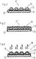
In
Ein Träger
Mit Linien sind Lichtkegel
Im in
In
Die erfindungsgemäßen Chip-On-Board-LED-Module
In
Die Füllhöhe des Silikons wird derart gewählt, dass der Träger
Das flüssige Silikon
In den
In
Die in
In
In
Alle genannten Merkmale, auch die den Zeichnungen allein zu entnehmenden sowie auch einzelne Merkmale, die in Kombination mit anderen Merkmalen offenbart sind, werden allein und in Kombination als erfindungswesentlich angesehen. Erfindungsgemäße Ausführungsformen können durch einzelne Merkmale oder eine Kombination mehrerer Merkmale erfüllt sein.All mentioned features, including the drawings alone to be taken as well as individual features that are disclosed in combination with other features are considered alone and in combination as essential to the invention. Embodiments of the invention may be accomplished by individual features or a combination of several features.
Bezugszeichenliste LIST OF REFERENCE NUMBERS
- 1, 1'1, 1 '
- unbeschichtetes Chip-On-Board-LED-Moduluncoated chip-on-board LED module
- 2, 2'2, 2 '
- Trägercarrier
- 3, 3'3, 3 '
- Leiterbahnconductor path
- 4, 4'4, 4 '
- LEDLED
- 5, 5'5, 5 '
- Lichtkegellight cone
- 66
- Stoßstellejoint
- 77
- Überlappungsbereichoverlap area
- 11–11'''11-11 '' '
- beschichtetes Chip-On-Board-LED-Modulcoated chip-on-board LED module
- 1212
- Silikonbeschichtungsilicone coating
- 1313
- Beschichtung der TrägerseitenflächenCoating of the carrier side surfaces
- 1515
- Linse aus SilikonSilicone lens
- 1616
- aufgeraute Oberflächenstrukturroughened surface texture
- 1717
- phosphoreszierendes Materialphosphorescent material
- 1818
- Licht verschiedener WellenlängenLight of different wavelengths
- 2020
- Gießformmold
- 2121
- flüssiges Silikonliquid silicone
- 2222
- Silikonvorratsilicone stock
ZITATE ENTHALTEN IN DER BESCHREIBUNG QUOTES INCLUDE IN THE DESCRIPTION
Diese Liste der vom Anmelder aufgeführten Dokumente wurde automatisiert erzeugt und ist ausschließlich zur besseren Information des Lesers aufgenommen. Die Liste ist nicht Bestandteil der deutschen Patent- bzw. Gebrauchsmusteranmeldung. Das DPMA übernimmt keinerlei Haftung für etwaige Fehler oder Auslassungen.This list of the documents listed by the applicant has been generated automatically and is included solely for the better information of the reader. The list is not part of the German patent or utility model application. The DPMA assumes no liability for any errors or omissions.
Zitierte PatentliteraturCited patent literature
- EP 1657758 A2[0012, 0017]EP 1657758 A2[0012, 0017]
Claims (13)
Translated fromGermanPriority Applications (11)
| Application Number | Priority Date | Filing Date | Title |
|---|---|---|---|
| DE102010044471ADE102010044471A1 (en) | 2010-09-06 | 2010-09-06 | Method for coating optoelectronic chip-on-board module for, e.g. high-power UV LED lamp, involves immersing optoelectronic component in carrier into silicone material, and curing and thermally cross-linking silicone material with carrier |
| CN201180042727.0ACN103109587B (en) | 2010-09-06 | 2011-08-29 | Coating method for optoelectronic chip-on-board modules |
| KR1020167008472AKR101660684B1 (en) | 2010-09-06 | 2011-08-29 | Coating method for an optoelectronic chip-on-board module |
| KR1020137005679AKR20130043685A (en) | 2010-09-06 | 2011-08-29 | Coating method for an optoelectronic chip-on-board module |
| EP11763584.7AEP2614694B1 (en) | 2010-09-06 | 2011-08-29 | Coating method for an optoelectronic chip-on-board module |
| JP2013527483AJP5882332B2 (en) | 2010-09-06 | 2011-08-29 | Coating methods for optoelectronic chip-on-board modules |
| PCT/EP2011/004326WO2012031703A1 (en) | 2010-09-06 | 2011-08-29 | Coating method for an optoelectronic chip-on-board module |
| US13/818,868US8956922B2 (en) | 2010-09-06 | 2011-08-29 | Coating method for an optoelectronic chip-on-board module |
| TW100132151ATWI518875B (en) | 2010-09-06 | 2011-09-06 | Photoelectric wafer direct package (CHIP-ON-BOARD) module coating method |
| US14/531,330US9269836B2 (en) | 2010-09-06 | 2014-11-03 | Optoelectronic chip-on-board module |
| JP2015214180AJP6279531B2 (en) | 2010-09-06 | 2015-10-30 | Coating methods for optoelectronic chip-on-board modules |
Applications Claiming Priority (1)
| Application Number | Priority Date | Filing Date | Title |
|---|---|---|---|
| DE102010044471ADE102010044471A1 (en) | 2010-09-06 | 2010-09-06 | Method for coating optoelectronic chip-on-board module for, e.g. high-power UV LED lamp, involves immersing optoelectronic component in carrier into silicone material, and curing and thermally cross-linking silicone material with carrier |
Publications (1)
| Publication Number | Publication Date |
|---|---|
| DE102010044471A1true DE102010044471A1 (en) | 2012-03-08 |
Family
ID=44719819
Family Applications (1)
| Application Number | Title | Priority Date | Filing Date |
|---|---|---|---|
| DE102010044471ACeasedDE102010044471A1 (en) | 2010-09-06 | 2010-09-06 | Method for coating optoelectronic chip-on-board module for, e.g. high-power UV LED lamp, involves immersing optoelectronic component in carrier into silicone material, and curing and thermally cross-linking silicone material with carrier |
Country Status (1)
| Country | Link |
|---|---|
| DE (1) | DE102010044471A1 (en) |
Cited By (7)
| Publication number | Priority date | Publication date | Assignee | Title |
|---|---|---|---|---|
| WO2013010634A1 (en) | 2011-07-18 | 2013-01-24 | Heraeus Noblelight Gmbh | Optoelectronic module with improved optical system |
| DE102011107895A1 (en) | 2011-07-18 | 2013-01-24 | Heraeus Noblelight Gmbh | Optoelectronic module with lens system |
| WO2013164052A1 (en)* | 2012-05-02 | 2013-11-07 | Heraeus Noblelight Gmbh | Method for producing an optical module having a silicone lens, optical module and use thereof |
| AT14904U1 (en)* | 2014-04-30 | 2016-08-15 | Tridonic Gmbh & Co Kg | Device for wrapping electrical components |
| EP3070396A1 (en)* | 2015-03-13 | 2016-09-21 | Hella KGaA Hueck & Co. | Light module |
| CN117621334A (en)* | 2023-11-28 | 2024-03-01 | 深圳视爵光旭电子有限公司 | A jig for display module production and its use method |
| EP4443526A4 (en)* | 2022-05-27 | 2025-03-19 | Boe Technology Group Co., Ltd. | Display substrate, mold assembly, tiled display module, and display device |
Citations (4)
| Publication number | Priority date | Publication date | Assignee | Title |
|---|---|---|---|---|
| EP1657758A2 (en) | 2004-11-15 | 2006-05-17 | LumiLeds Lighting U.S., LLC | Light emitting diode with molded lens and method of manufacturing the same |
| US20070045761A1 (en)* | 2005-08-26 | 2007-03-01 | Lumileds Lighting U.S, Llc | Color converted light emitting diode |
| US20080230797A1 (en)* | 2007-03-21 | 2008-09-25 | Hui-Hung Chang | LED module and manufacturing method thereof |
| US20100065983A1 (en)* | 2007-02-27 | 2010-03-18 | Towa Corporation | Method of compression-molding light-emitting elements |
- 2010
- 2010-09-06DEDE102010044471Apatent/DE102010044471A1/ennot_activeCeased
Patent Citations (4)
| Publication number | Priority date | Publication date | Assignee | Title |
|---|---|---|---|---|
| EP1657758A2 (en) | 2004-11-15 | 2006-05-17 | LumiLeds Lighting U.S., LLC | Light emitting diode with molded lens and method of manufacturing the same |
| US20070045761A1 (en)* | 2005-08-26 | 2007-03-01 | Lumileds Lighting U.S, Llc | Color converted light emitting diode |
| US20100065983A1 (en)* | 2007-02-27 | 2010-03-18 | Towa Corporation | Method of compression-molding light-emitting elements |
| US20080230797A1 (en)* | 2007-03-21 | 2008-09-25 | Hui-Hung Chang | LED module and manufacturing method thereof |
Cited By (11)
| Publication number | Priority date | Publication date | Assignee | Title |
|---|---|---|---|---|
| WO2013010634A1 (en) | 2011-07-18 | 2013-01-24 | Heraeus Noblelight Gmbh | Optoelectronic module with improved optical system |
| DE102011107895A1 (en) | 2011-07-18 | 2013-01-24 | Heraeus Noblelight Gmbh | Optoelectronic module with lens system |
| DE102011107893A1 (en) | 2011-07-18 | 2013-01-24 | Heraeus Noblelight Gmbh | Optoelectronic module with improved optics |
| WO2013010636A1 (en) | 2011-07-18 | 2013-01-24 | Heraeus Noblelight Gmbh | Optoelectronic module comprising a lens system |
| US9640579B2 (en) | 2011-07-18 | 2017-05-02 | Heraeus Noblelight Gmbh | Optoelectronic module comprising a lens system |
| WO2013164052A1 (en)* | 2012-05-02 | 2013-11-07 | Heraeus Noblelight Gmbh | Method for producing an optical module having a silicone lens, optical module and use thereof |
| AT14904U1 (en)* | 2014-04-30 | 2016-08-15 | Tridonic Gmbh & Co Kg | Device for wrapping electrical components |
| EP3070396A1 (en)* | 2015-03-13 | 2016-09-21 | Hella KGaA Hueck & Co. | Light module |
| WO2016146408A1 (en) | 2015-03-13 | 2016-09-22 | Hella Kgaa Hueck & Co. | Light module |
| EP4443526A4 (en)* | 2022-05-27 | 2025-03-19 | Boe Technology Group Co., Ltd. | Display substrate, mold assembly, tiled display module, and display device |
| CN117621334A (en)* | 2023-11-28 | 2024-03-01 | 深圳视爵光旭电子有限公司 | A jig for display module production and its use method |
Similar Documents
| Publication | Publication Date | Title |
|---|---|---|
| EP2614693B1 (en) | Method for coating an optoelectronic chip-on-board module and optoelectronic chip-on-board-module | |
| EP2614694B1 (en) | Coating method for an optoelectronic chip-on-board module | |
| DE102010044471A1 (en) | Method for coating optoelectronic chip-on-board module for, e.g. high-power UV LED lamp, involves immersing optoelectronic component in carrier into silicone material, and curing and thermally cross-linking silicone material with carrier | |
| EP2844447B1 (en) | Process for the manufacture of an optical module with silicone optics, optical module and its use | |
| EP2735025B1 (en) | Optoelectronic module comprising a lens system | |
| DE102011107893A1 (en) | Optoelectronic module with improved optics | |
| DE102012212963B4 (en) | Process for producing an optoelectronic semiconductor component | |
| DE102018128325B4 (en) | Optical device and light source module in which it is contained | |
| DE102009058006A1 (en) | Optoelectronic semiconductor device | |
| DE102006048592A1 (en) | Optoelectronic module and method for producing an optoelectronic module | |
| DE102011107892A1 (en) | Method for coating e.g. chip-on-board UV-LED module utilized in solar cell, involves curing and cross-linking liquid silicone with optoelectronic components and carriers, and removing carrier with hardened silicone coating from mold | |
| EP2308105B1 (en) | Optoelectronic semiconductor component | |
| DE102008048846B4 (en) | optoelectronic component | |
| EP2844448A1 (en) | Method for producing an optical module having a polymer lens, optical module and use thereof | |
| WO2020094442A1 (en) | Optoelectronic semiconductor component, and method for producing an optoelectronic semiconductor component | |
| DE102010044560A1 (en) | Method for producing an optoelectronic semiconductor component | |
| DE102007023583A1 (en) | Photovoltaic device with optical elements for deflecting incident solar radiation in a given spectral range on laterally mounted solar cells on the optical elements | |
| DE102010047156A1 (en) | Optoelectronic component and method for producing an optoelectronic component | |
| WO2017198547A1 (en) | Module for a video wall having a film | |
| DE102008044847A1 (en) | Optoelectronic component | |
| DE112022002009B4 (en) | METHOD FOR PRODUCING AN OPTOELECTRONIC COMPONENT | |
| DE112020000587T5 (en) | Spectroscope and spectroscope manufacturing process | |
| DE102018129191A1 (en) | METHOD FOR PRODUCING AN ILLUMINATOR | |
| DE102011100028A1 (en) | Component and method for manufacturing a device | |
| DE102015120855B4 (en) | Method for producing an optoelectronic component and optoelectronic component |
Legal Events
| Date | Code | Title | Description |
|---|---|---|---|
| R016 | Response to examination communication | ||
| R016 | Response to examination communication | ||
| R082 | Change of representative | Representative=s name:BRAND, NORMEN, DR. RER. NAT., DE Representative=s name:BRAND, NORMEN, DIPL.-CHEM. UNIV. DR. RER. NAT., DE Representative=s name:EULER, MATTHIAS, DR., DE | |
| R082 | Change of representative | Representative=s name:BRAND, NORMEN, DR. RER. NAT., DE Representative=s name:BRAND, NORMEN, DIPL.-CHEM. UNIV. DR. RER. NAT., DE | |
| R002 | Refusal decision in examination/registration proceedings | ||
| R003 | Refusal decision now final |