DE102010011517A1 - Laminate construction for a chip card and method for its production - Google Patents
Laminate construction for a chip card and method for its productionDownload PDFInfo
- Publication number
- DE102010011517A1 DE102010011517A1DE102010011517ADE102010011517ADE102010011517A1DE 102010011517 A1DE102010011517 A1DE 102010011517A1DE 102010011517 ADE102010011517 ADE 102010011517ADE 102010011517 ADE102010011517 ADE 102010011517ADE 102010011517 A1DE102010011517 A1DE 102010011517A1
- Authority
- DE
- Germany
- Prior art keywords
- layer
- chip module
- adhesive material
- base
- transponder
- Prior art date
- Legal status (The legal status is an assumption and is not a legal conclusion. Google has not performed a legal analysis and makes no representation as to the accuracy of the status listed.)
- Withdrawn
Links
Images

Classifications
- G—PHYSICS
- G06—COMPUTING OR CALCULATING; COUNTING
- G06K—GRAPHICAL DATA READING; PRESENTATION OF DATA; RECORD CARRIERS; HANDLING RECORD CARRIERS
- G06K19/00—Record carriers for use with machines and with at least a part designed to carry digital markings
- G06K19/06—Record carriers for use with machines and with at least a part designed to carry digital markings characterised by the kind of the digital marking, e.g. shape, nature, code
- G06K19/067—Record carriers with conductive marks, printed circuits or semiconductor circuit elements, e.g. credit or identity cards also with resonating or responding marks without active components
- G06K19/07—Record carriers with conductive marks, printed circuits or semiconductor circuit elements, e.g. credit or identity cards also with resonating or responding marks without active components with integrated circuit chips
- G06K19/077—Constructional details, e.g. mounting of circuits in the carrier
- G06K19/0772—Physical layout of the record carrier
- G06K19/07722—Physical layout of the record carrier the record carrier being multilayered, e.g. laminated sheets
- G—PHYSICS
- G06—COMPUTING OR CALCULATING; COUNTING
- G06K—GRAPHICAL DATA READING; PRESENTATION OF DATA; RECORD CARRIERS; HANDLING RECORD CARRIERS
- G06K19/00—Record carriers for use with machines and with at least a part designed to carry digital markings
- G06K19/06—Record carriers for use with machines and with at least a part designed to carry digital markings characterised by the kind of the digital marking, e.g. shape, nature, code
- G06K19/067—Record carriers with conductive marks, printed circuits or semiconductor circuit elements, e.g. credit or identity cards also with resonating or responding marks without active components
- G06K19/07—Record carriers with conductive marks, printed circuits or semiconductor circuit elements, e.g. credit or identity cards also with resonating or responding marks without active components with integrated circuit chips
- G06K19/077—Constructional details, e.g. mounting of circuits in the carrier
- G06K19/07745—Mounting details of integrated circuit chips
- H—ELECTRICITY
- H01—ELECTRIC ELEMENTS
- H01L—SEMICONDUCTOR DEVICES NOT COVERED BY CLASS H10
- H01L23/00—Details of semiconductor or other solid state devices
- H01L23/28—Encapsulations, e.g. encapsulating layers, coatings, e.g. for protection
- H—ELECTRICITY
- H01—ELECTRIC ELEMENTS
- H01Q—ANTENNAS, i.e. RADIO AERIALS
- H01Q1/00—Details of, or arrangements associated with, antennas
- H01Q1/12—Supports; Mounting means
- H—ELECTRICITY
- H01—ELECTRIC ELEMENTS
- H01L—SEMICONDUCTOR DEVICES NOT COVERED BY CLASS H10
- H01L2924/00—Indexing scheme for arrangements or methods for connecting or disconnecting semiconductor or solid-state bodies as covered by H01L24/00
- H01L2924/0001—Technical content checked by a classifier
- H01L2924/0002—Not covered by any one of groups H01L24/00, H01L24/00 and H01L2224/00
Landscapes
- Engineering & Computer Science (AREA)
- Computer Hardware Design (AREA)
- Microelectronics & Electronic Packaging (AREA)
- Physics & Mathematics (AREA)
- General Physics & Mathematics (AREA)
- Theoretical Computer Science (AREA)
- Condensed Matter Physics & Semiconductors (AREA)
- Power Engineering (AREA)
- Credit Cards Or The Like (AREA)
Abstract
Translated fromGermanDescription
Translated fromGermanDie vorliegende Erfindung betrifft einen Laminataufbau für eine Chipkarte mit einer Basislage, einem zumindest anteilig in der Basislage aufgenommenen Chipmodul und zumindest einer die Basislage abdeckenden Decklage, wobei ein zwischen dem Chipmodul und der Decklage sowie dem Chipmodul und der Basislage ausgebildeter Zwischenraum mit einem Klebermaterial verfüllt ist. Darüber hinaus betrifft die Erfindung ein Verfahren zur Herstellung eines derartigen Laminataufbaus.The present invention relates to a laminate structure for a chip card having a base layer, a chip module accommodated at least partially in the base layer and at least one cover layer covering the base layer, wherein a gap formed between the chip module and the cover layer and the chip module and the base layer is filled with an adhesive material , Moreover, the invention relates to a method for producing such a laminate structure.
Chipkarten unterliegen unabhängig von ihrer Ausbildung als Kontaktkarte oder kontaktlose Karte im Gebrauch einer wechselnden Biegebeanspruchung, die häufig dazu führt, dass es zu Rissbildungen und Delaminationen im Laminataufbau kommt. Als insbesondere gefährdet erweist sich dabei der Bereich der Chipkarte, der das Chipmodul aufnimmt, da es infolge einer dynamischen Biegebelastung zu einer Relativbewegung zwischen dem Chipmodul und den angrenzenden Lagen oder Schichten des Laminataufbaus kommen kann.Chip cards, regardless of their contact card or contactless card design, undergo alternating bending stress in use, which often results in cracking and delamination in the laminate build-up. In particular, the area of the chip card receiving the chip module proves to be particularly endangered because, as a result of a dynamic bending load, a relative movement can occur between the chip module and the adjacent layers or layers of the laminate structure.
Dieses bekannte Phänomen führt dazu, dass Chipkarten in der Regel nur eine sehr begrenzte Lebensdauer aufweisen, die zwar in vielen Fällen einem Gebrauch von Chipkarten nicht entgegensteht, insbesondere in den Fällen, in denen ohnehin nur eine zeitlich sehr begrenzte Verwendung der Chipkarten, wie es beispielsweise bei Kreditkarten oder Telefonkarten der Fall ist, beabsichtigt ist. Andere Anwendungsbereiche scheinen jedoch aufgrund dieser begrenzten Lebensdauer Chipkarten von einem Einsatz auszuschließen.This known phenomenon means that smart cards usually have only a very limited life, which in many cases does not preclude the use of smart cards, especially in cases where anyway only a very limited use of the chip cards, as it for example is the case with credit cards or phone cards, is intended. However, other applications appear to exclude smart cards from deployment due to this limited lifetime.
Insbesondere trifft dies für den Bereich der Ausweisdokumente zu, wenn man davon ausgeht, dass personalisierte Ausweisdokumente, wie beispielsweise Personalausweise, in der Regel für eine Dauer von zehn Jahren ausgestellt werden. Zwar hat man bereits festgestellt, dass sich bestimmte Materialien, wie beispielsweise Polycarbonat, in besonderer Weise als Lagenmaterial für die Herstellung eines Laminataufbaus eignen, da Polycarbonat unabhängig von einer dynamischen Beanspruchung bereits grundsätzlich eine höhere Alterungsbeständigkeit aufweist als PVC, das in der Regel bereits nach vier bis fünf Jahren alterungsbedingte Risse aufweist und sich daher grundsätzlich weniger zur Herstellung von Chipkarten eignet, die eine höhere Lebensdauer aufweisen müssen.In particular, this applies to the field of identity documents, assuming that personalized identity documents, such as identity cards, are usually issued for a period of ten years. Although it has already been found that certain materials, such as polycarbonate, are particularly suitable as a layer material for the production of a laminate structure, since polycarbonate regardless of a dynamic stress already has a higher resistance to aging than PVC, which usually already after four Age-related cracks up to five years and therefore less suitable for the production of smart cards, which must have a longer life.
Polycarbonat weist jedoch den Nachteil auf, dass es bei Verwendung als Lagenmaterial eines Laminataufbaus aufgrund der bereits vorstehend erwähnten Relativbewegungen zwischen dem Chipmodul und dem Laminataufbau zu einer Ausbildung von Rissen im Inneren des Laminataufbaus kommen kann, wobei sich derartige Risse nach ihrem Entstehen schnell durch den Laminataufbau ausbreiten und dann auch die Kartenoberfläche erreichen.However, polycarbonate has the disadvantage that, when used as a layer material of a laminate structure due to the above-mentioned relative movements between the chip module and the laminate structure can lead to the formation of cracks in the interior of the laminate structure, such cracks quickly after their emergence by the laminate structure spread out and then reach the map surface.
Bei der Herstellung von Chipkarten werden regelmäßig so genannte Füllermaterialien verwendet, die dazu dienen, ein in eine Fensteröffnung eines Laminataufbaus eingesetztes Chipmodul im Laminataufbau bzw. der Fensteröffnung definiert anzuordnen. Die hierzu verwendeten in der Regel auf Epoxy-Basis hergestellten Füllermaterialien ermöglichen es zwar, eine Ausfüllung von zwischen dem Chipmodul und der Fensteröffnung ausgebildeten Zwischenräumen herzustellen, so dass zumindest anfänglich eine Fixierung des Chipmoduls im Laminataufbau möglich ist. Durch dieses Ausfüllen der Zwischenräume wird zumindest zeitweise ein definierter Formschluss zwischen dem Chipmodul und der Fensteröffnung im Laminataufbau ermöglicht. Jedoch erweist sich dieser Formschluss als offensichtlich nicht ausreichend, um zwischen dem Chipmodul und dem umgebenden Laminataufbau einen Kraftschluss zu ermöglichen, der auch wechselnden Biegebeanspruchungen über einen ausreichend langen Zeitraum Stand hält.In the production of chip cards, so-called filler materials are used regularly, which serve to arrange a chip module inserted into a window opening of a laminate structure in the laminate structure or the window opening in a defined manner. Although the filler materials produced for this purpose, which are generally produced on the basis of epoxy, make it possible to fill in intermediate spaces formed between the chip module and the window opening, at least initially a fixation of the chip module in the laminate structure is possible. By filling in the intermediate spaces, a defined form fit between the chip module and the window opening in the laminate structure is made possible at least temporarily. However, this form fit proves to be obviously insufficient to allow between the chip module and the surrounding laminate structure a frictional connection, which also withstands alternating bending stresses over a sufficiently long period of time.
Aufgabe der vorliegenden Erfindung ist es daher, einen Laminataufbau für eine Chipkarte sowie ein Verfahren zu dessen Herstellung vorzuschlagen, die bzw. das die Herstellung von Chipkarten mit verbesserter Rissbeständigkeit und damit erhöhter Lebensdauer ermöglicht.Object of the present invention is therefore to propose a laminate structure for a smart card and a method for its production, which or the production of chip cards with improved crack resistance and thus increased life allows.
Zur Lösung dieser Aufgabe weist der erfindungsgemäße Laminataufbau die Merkmale des Anspruchs 1 auf. Das erfindungsgemäße Verfahren weist die Merkmale des Anspruchs 11 auf.To solve this problem, the laminate structure according to the invention has the features of claim 1. The inventive method has the features of claim 11.
Erfindungsgemäß wird für den Laminataufbau ein Klebermaterial verwendet, das sowohl Adhäsionskräfte gegenüber den Oberflächen der Basislage und der Decklage als auch Adhäsionskräfte gegenüber den Oberflächen des Chipmoduls ausbildet. Aufgrund der vorstehenden Eigenschaften ist das Klebermaterial in der Lage, zwischen dem Chipmodul und dem das Chipmodul umgebenden Laminataufbau einen Kraftschluss herzustellen, so dass im Unterschied zu den auf Epoxy-Basis hergestellten Füllermaterialien nicht nur eine Ausfüllung von Zwischenräumen zur Herstellung eines Formschlusses erreicht wird, sondern tatsächlich eine kraftschlüssige Verbindung, die auch wechselnden Biegebeanspruchungen zwischen dem Chipmodul und dem umgebenden Laminataufbau Stand hält. Somit sind Relativbewegungen des Chipmoduls gegenüber dem umgebenden Laminataufbau nicht möglich. Eine entsprechend induzierte Rissbildung wird somit wirksam vermieden.According to the invention, an adhesive material is used for the laminate structure, which forms both adhesion forces against the surfaces of the base layer and the cover layer as well as adhesion forces with respect to the surfaces of the chip module. Due to the above properties, the adhesive material is able to produce a frictional connection between the chip module and the laminate structure surrounding the chip module, so that, in contrast to the epoxy-based filler materials not only a filling of gaps for producing a positive connection is achieved, but actually a non-positive connection, which also withstands alternating bending stresses between the chip module and the surrounding laminate structure. Thus, relative movements of the chip module relative to the surrounding laminate structure are not possible. A correspondingly induced cracking is thus effectively avoided.
Insbesondere wird durch die einhüllende Anordnung des Chipmoduls in das Klebermaterial eine quasi monolithische Aufnahmestruktur für das Chipmodul geschaffen, so dass bei Biegebeanspruchung der Karte im Wesentlichen alle Biege- und Scherbelastungen durch diese sowohl kraftschlüssig mit dem Chipmodul als auch kraftschlüssig mit der Umgebung des Chipmoduls verbundene Struktur über den Umfang der Struktur aufgenommen werden.In particular, by the enveloping arrangement of the chip module in the adhesive material a created virtually monolithic receiving structure for the chip module, so that when bending stress of the card substantially all bending and shear loads are taken by these both non-positively connected to the chip module and non-positively connected to the environment of the chip module structure over the circumference of the structure.
Vorzugsweise wird das Klebermaterial so gewählt, dass das Verhältnis der gegenüber der Basislage und der Decklage ausgebildeten Adhäsionskräfte zu den gegenüber dem Chipmodul ausgebildeten Adhäsionskräften 0,5 bis 1,5 beträgt. Somit ist sichergestellt, dass die Adhäsionskräfte gegenüber der Decklage bzw. der Basislage und die Adhäsionskräfte gegenüber dem Chipmodul eine vergleichbare Größe aufweisen, so dass unabhängig von der Art des Materialübergangs, also unabhängig davon, ob es sich um einen Materialübergang vom Klebermaterial auf die Decklage bzw. Basislage oder vom Klebermaterial auf das Chipmodul handelt, für einen ausreichenden Kraftschluss gesorgt ist.Preferably, the adhesive material is selected such that the ratio of the adhesion forces formed with respect to the base layer and the cover layer to the adhesion forces formed with respect to the chip module is 0.5 to 1.5. This ensures that the adhesion forces with respect to the cover layer or the base layer and the adhesion forces have a comparable size to the chip module, so that regardless of the type of material transition, ie regardless of whether it is a material transfer from the adhesive material to the cover layer or Base layer or the adhesive material on the chip module is, is provided for a sufficient adhesion.
Besonders vorteilhaft ist es, wenn das Klebermaterial auf Acrylatbasis hergestellt ist.It is particularly advantageous if the adhesive material is produced on an acrylate basis.
Vorzugsweise weist das Klebermaterial mehr als 50 Gewichtsprozent Acrylat auf.Preferably, the adhesive material has greater than 50 weight percent acrylate.
Insbesondere hinsichtlich des Herstellungsverfahrens für den Laminataufbau erweist es sich als vorteilhaft, wenn das Klebermaterial aus einem beidseitig mit einer Acrylatbeschichtung versehenen Lagenmaterial hergestellt ist.In particular, with regard to the manufacturing process for the laminate structure, it proves to be advantageous if the adhesive material is made of a layer material provided on both sides with an acrylate coating.
Grundsätzlich ist festzustellen, dass sich der Laminataufbau unabhängig von der Art der Chipkarte als vorteilhaft erweist, wenn es darum geht, die Rissbildung im Kartenkörper zu vermeiden. Besonders vorteilhaft wirken sich jedoch die eingangs bereits geschilderten, positiven Eigenschaften aus, wenn die Basislage des Laminataufbaus als Transponderlage ausgebildet ist mit einer auf der Transponderlage ausgebildeten Antennenanordnung, deren Kontaktenden mit Anschlussflächen des Chips kontaktiert sind.Basically, it should be noted that the laminate structure, regardless of the type of chip card proves to be advantageous when it comes to avoid cracking in the card body. However, the positive properties already described at the outset have a particularly advantageous effect if the base layer of the laminate structure is designed as a transponder layer with an antenna arrangement formed on the transponder layer whose contact ends are in contact with connection surfaces of the chip.
Bei einem derartigen Laminataufbau, der die Herstellung einer kontaktlosen Chipkarte ermöglicht, ist ein belastbarer Kraftschluss zwischen dem Chipmodul und den umgebenden Lagen des Laminataufbaus besonders wichtig, da derartige als Ausweisdokumente, insbesondere Personalausweise, verwendete Chipkarten eine besonders hohe Lebensdauer und Zuverlässigkeit aufweisen müssen.In such a laminate structure, which allows the production of a contactless chip card, a strong adhesion between the chip module and the surrounding layers of the laminate structure is particularly important, since such as identity documents, in particular identity cards, used smart cards must have a particularly high durability and reliability.
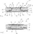
Vorzugsweise ist hierbei das Chipmodul auf seiner Oberseite von einer auf der Decklage angeordneten Oberlage und auf seiner Unterseite von einer auf der Transponderlage angeordneten Unterlage bedeckt, wobei zumindest eine in der Decklage ausgebildete Fensteröffnung und eine in der Transponderlage ausgebildete Fensteröffnung, die einen Aufnahmeraum zur Anordnung des Chipmoduls definieren, jeweils mit einem sich zwischen der Oberseite des Chipmoduls und der Oberlage sowie zwischen der Unterseite des Chipmoduls und der Unterlage erstreckenden Klebermaterialauftrag abgedeckt sind.Preferably, the chip module is covered on its upper side by a top layer arranged on the cover layer and on its underside by a substrate disposed on the transponder layer, at least one window opening formed in the cover layer and a window opening formed in the transponder layer having a receiving space for the arrangement of the Define chip module, each covered with an extending between the top of the chip module and the top layer and between the bottom of the chip module and the base adhesive material order.
Eine derartige zwischen Klebermaterialaufträgen ausgebildete „Sandwichlage” des Chipmoduls ermöglicht eine besonders sichere und dauerhaft haltbare Anordnung des Chipmoduls im Laminataufbau, bei der Relativbewegungen des Chipmoduls wirksam durch den beidseitigen Klebermaterialauftrag vermieden werden.Such a "sandwich layer" of the chip module formed between adhesive material applications makes possible a particularly secure and permanently durable arrangement of the chip module in the laminate structure, in which relative movements of the chip module are effectively prevented by the adhesive material application on both sides.
Dies gilt unabhängig davon, ob die Transponderlage und die Decklage im Ausgangszustand als voneinander unabhängige Lagen ausgebildet sind, oder ob stattdessen eine einstückig ausgebildete Inlaylage verwendet wird.This applies regardless of whether the transponder layer and the cover layer are formed in the initial state as mutually independent layers, or whether instead of an integrally formed inlay layer is used.
Eine kraftschlüssige Aufnahme des Chipmoduls im Laminataufbau mit gleichzeitig möglichst großflächig ausgebildeten Krafteinleitungen zwischen dem Klebermaterialauftrag und der Umgebung wird möglich, wenn der auf der Oberseite des Chipmoduls angeordnete Klebermaterialauftrag und der auf der Unterseite des Chipmoduls angeordnete Klebermaterialauftrag sich jeweils über den Rand der Fensteröffnung hinaus zwischen der Oberlage und der Decklage sowie zwischen der Unterlage und der Transponderlage erstrecken.A frictional recording of the chip module in the laminate structure with simultaneously formed as large as possible force applications between the Klebermaterialauftrag and the environment is possible if the arranged on the top of the chip module adhesive material application and arranged on the underside of the chip module adhesive material each time over the edge of the window opening between the Upper layer and the top layer and between the pad and the transponder position extend.
Besonders vorteilhaft treten die Vorzüge des erfindungsgemäßen Laminataufbaus in Erscheinung, wenn zumindest die Basislage und/oder die Decklage aus Polycarbonat gebildet sind.The advantages of the laminate structure according to the invention are particularly advantageous if at least the base layer and / or the cover layer are formed from polycarbonate.
Bei dem erfindungsgemäßen Verfahren zur Herstellung eines Laminataufbaus für eine Chipkarte mit einer Basislage, einem zumindest anteilig in der Basislage aufgenommenen Chipmodul und zumindest einer die Basislage abdeckenden Decklage, wird vor einem Laminiervorgang zur Herstellung eines Laminatverbunds zwischen der Decklage und dem Chipmodul sowie zwischen der Basislage und dem Chipmodul ein Klebermaterialdepot angeordnet, dessen Volumen derart bemessen ist, dass ein zwischen dem Chipmodul und der Decklage sowie zwischen dem Chipmodul und der Basislage ausgebildeter Zwischenraum während des Laminiervorgangs mit dem Klebermaterial verfüllt wird, wobei als Klebermaterial ein Klebermaterial verwendet wird, das sowohl Adhäsionskräfte zu den während des Laminiervorgangs benetzten Oberflächen der Basislage und der Decklage als auch Adhäsionskräfte zu den benetzten Oberflächen des Chipmoduls ausbildet.In the method according to the invention for producing a laminate structure for a chip card with a base layer, a chip module accommodated at least partially in the base layer and at least one cover layer covering the base layer, a laminating process is used to produce a laminate composite between the cover layer and the chip module and between the base layer and the chip module an adhesive material depot arranged whose volume is such that a space formed between the chip module and the cover layer and between the chip module and the base layer gap is filled during the lamination with the adhesive material, wherein an adhesive material is used as the adhesive material, the adhesive forces both forms the surfaces of the base layer and the cover layer which are wetted during the laminating process, as well as adhesion forces to the wetted surfaces of the chip module.
Bei dem erfindungsgemäßen Verfahren erfolgt bereits vor Durchführung des eigentlichen Laminiervorgangs eine Bereitstellung von Klebermaterialdepots an unterschiedlichen Stellen des Laminataufbaus, nämlich zum einen der Unterseite des Chipmoduls zugeordnet und zum anderen der Oberseite des Chipmoduls zugeordnet, so dass im nachfolgenden Laminiervorgang eine besonders gleichmäßige Verteilung des Klebermaterials erreicht wird, mit der Folge, dass die vorteilhaft vom Klebermaterial sowohl gegenüber den Lagen des Laminataufbaus als auch gegenüber dem Chipmodul ausgebildeten Adhäsionskräfte eine entsprechende Verteilung im Laminataufbau erreichen. In the method according to the invention, even before the actual lamination process is carried out, adhesive material deposits are made available at different points of the laminate structure, namely assigned to the lower side of the chip module and assigned to the upper side of the chip module, so that a particularly even distribution of the adhesive material is achieved in the subsequent lamination process becomes, with the result that the adhesion forces formed advantageously by the adhesive material both with respect to the layers of the laminate structure and with respect to the chip module achieve a corresponding distribution in the laminate structure.
Besonders vorteilhaft erweist es sich dabei, wenn das Klebermaterialdepot als Klebermateriallage ausgebildet ist, die in einem im Lagenaufbau zur Aufnahme des Chipmoduls ausgebildeten Aufnahmeraum eingelegt wird, derart, dass die Klebermateriallage die den Aufnahmeraum begrenzende Oberfläche bedeckt. Somit kann beispielsweise im Fall einer als Kontaktkarte ausgebildeten Chipkarte, bei der das Chipmodul in einer zur Außenseite des Kartenkörpers hin geöffneten Fensteröffnung aufgenommen ist, das Klebermaterialdepot als Auskleidung der Fensteröffnung vor Durchführung des Laminiervorgangs eingelegt werden, anschließend das Chipmodul in die durch die Klebermateriallage ausgekleidete Fensteröffnung eingesetzt werden und schließlich in dem nachfolgenden Laminiervorgang ein Laminatverbund zwischen der Decklage und der Basislage und dem Chipmodul über die Klebermateriallage hergestellt werden.In this case, it proves to be particularly advantageous if the adhesive material depot is designed as an adhesive material layer which is inserted in a receiving space formed in the layer structure for receiving the chip module, such that the adhesive material layer covers the surface delimiting the receiving space. Thus, for example, in the case of a chip card designed as a contact card, in which the chip module is received in a window opening opened to the outside of the card body, the adhesive material depot can be inserted as a lining of the window opening before the lamination process is carried out, then the chip module is inserted into the window opening lined by the adhesive material layer Finally, in the subsequent lamination process, a laminate composite is produced between the cover layer and the base layer and the chip module via the adhesive material layer.
Wenn dabei die Klebermateriallage derart in den Aufnahmeraum eingelegt wird, dass Ränder der Klebermateriallage die Oberfläche der Decklage überragen, ist sichergestellt, dass durch den nachfolgenden Laminiervorgang ein flächenbündiger und von Fehlstellen freier Übergang zwischen einer äußeren Kontaktoberfläche des Chipmoduls und der angrenzenden Decklage ausgebildet ist.In this case, if the adhesive material layer is inserted into the receiving space in such a way that edges of the adhesive material layer project beyond the surface of the cover layer, it is ensured that a flush and defect-free transition between an outer contact surface of the chip module and the adjacent cover layer is formed by the subsequent laminating process.
Wenn das Verfahren zur Herstellung einer kontaktlosen Chipkarte eingesetzt wird, ist es besonders vorteilhaft, wenn bei Ausbildung der Basislage als Transponderlage mit einer auf der Transponderlage ausgebildeten Antennenanordnung, deren Kontaktenden mit Anschlussflächen des Chipmoduls kontaktiert sind, das Klebermaterialdepot als eine Klebermateriallage ausgebildet ist, die zwischen einer Oberseite des Chipmoduls und einer die Decklage bedeckenden Oberlage sowie zwischen der Unterseite des Chipmoduls und einer die Transponderlage bedeckenden Unterlage angeordnet wird, wobei die Klebermateriallage mit ihren Rändern über eine in der Decklage und der Transponderlage jeweils ausgebildete Fensteröffnung hinausragt.When the method for producing a contactless chip card is used, it is particularly advantageous if, when the base layer is formed as a transponder layer with an antenna arrangement formed on the transponder layer, the contact ends of which are contacted with contact surfaces of the chip module, the adhesive material depot is formed as an adhesive material layer between an upper side of the chip module and a cover layer covering the top layer and between the underside of the chip module and a transponder layer covering the base is arranged, wherein the adhesive material layer protrudes with their edges on a respectively formed in the top layer and the transponder layer window opening.
Abgesehen davon, dass gemäß dieser bevorzugten Verfahrensvariante ein Laminataufbau für eine kontaktlose Chipkarte geschaffen wird, bei der sich das Chipmodul sandwichartig zwischen zwei Klebermateriallagen aufgenommen befindet, ermöglicht diese Verfahrensvariante es, wahlweise das als Klebermateriallage ausgebildete Klebermaterialdepot vor dem Laminiervorgang entweder auf die Oberseite und die Unterseite des Chipmoduls aufzutragen oder die Klebermateriallage auf die jeweils dem Chipmodul zugewandte Seite der Oberlage bzw. der Unterlage aufzubringen.Apart from the fact that according to this preferred variant of the method, a laminate structure is provided for a contactless chip card, in which the chip module is sandwiched between two layers of adhesive material, this method variant allows either the adhesive material deposit formed as an adhesive material layer to be applied to the top side and the bottom side before the lamination process of the chip module or to apply the adhesive material layer to the respective side of the top layer or the base facing the chip module.
Insbesondere die letztgenannte Verfahrensvariante, also die Aufbringung der Klebermateriallagen auf die Unterlage bzw. die Oberlage ermöglicht es, die jeweiligen Klebermateriallagen in einer Fertigungslinie, in der die verschiedenen Lagen des Laminataufbaus als linienförmig ausgebildete Endlos-Materiallagen zugefüllt werden, die Applikation der Klebermateriallagen auf die Unterlage und die Oberlage des Laminataufbaus vor einer Zusammenführung der Materiallagen durchzuführen, so dass beispielsweise die Applikation der Materiallagen synchron zur Herstellung der Fensteröffnungen in der Decklage erfolgen kann.In particular, the last-mentioned method variant, ie the application of the adhesive material layers to the substrate or the top layer, makes it possible to apply the adhesive material layers to the substrate in a production line in which the various layers of the laminate structure are filled as linearly formed endless material layers and perform the upper layer of the laminate structure before merging the layers of material, so that, for example, the application of the layers of material can be synchronized with the production of the window openings in the top layer.
Die Klebermateriallagen können als Kleberflecken (adhesive patch) – und damit unabhängig handhabbar – ausgebildet auf die Unterlage und die Oberlage aufgebracht werden oder alternativ auf eine Ober- und Unterseite des Chipmoduls aufgebracht werden.The adhesive material layers can be applied as adhesive dots (adhesive patch) - and thus independently handled - formed on the substrate and the top layer or alternatively applied to a top and bottom of the chip module.
Nachfolgend werden bevorzugte Ausführungsformen des Laminataufbaus anhand der Zeichnungen näher erläutert. Es zeigen:Hereinafter, preferred embodiments of the laminate structure are explained in more detail with reference to the drawings. Show it:
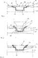
Wie
Wie weiter
Auf der Transponderlage
Wie ferner aus
Zwischen einer Unterseite
Die Klebermateriallagen
Wie
Nachfolgend dem Laminiervorgang erfolgt dann in an sich bekannter Art und Weise eine Vereinzelung der Chipkarten
Claims (16)
Translated fromGermanPriority Applications (11)
| Application Number | Priority Date | Filing Date | Title |
|---|---|---|---|
| DE102010011517ADE102010011517A1 (en) | 2010-03-15 | 2010-03-15 | Laminate construction for a chip card and method for its production |
| JP2012557425AJP2013522738A (en) | 2010-03-15 | 2011-02-17 | Laminated structure for chip card and manufacturing method thereof |
| AU2011229541AAU2011229541A1 (en) | 2010-03-15 | 2011-02-17 | Laminate structure for a chip card and method for the production thereof |
| CA2790932ACA2790932A1 (en) | 2010-03-15 | 2011-02-17 | Laminate structure for a chip card and method for the production thereof |
| EP11707081AEP2548158A1 (en) | 2010-03-15 | 2011-02-17 | Laminate structure for a chip card and method for the production thereof |
| US13/634,291US20130277432A1 (en) | 2010-03-15 | 2011-02-17 | Laminate Structure for a Chip Card and Method for the Production Thereof |
| KR1020127026166AKR20130012019A (en) | 2010-03-15 | 2011-02-17 | Laminate structure for a chip card and method for the production thereof |
| BR112012023155ABR112012023155A2 (en) | 2010-03-15 | 2011-02-17 | laminated structure for a chip card and method for producing it |
| MX2012010460AMX2012010460A (en) | 2010-03-15 | 2011-02-17 | Laminate structure for a chip card and method for the production thereof. |
| PCT/EP2011/000752WO2011113511A1 (en) | 2010-03-15 | 2011-02-17 | Laminate structure for a chip card and method for the production thereof |
| ZA2012/06797AZA201206797B (en) | 2010-03-15 | 2012-09-11 | Laminate structure for a chip card and method for the production thereof |
Applications Claiming Priority (1)
| Application Number | Priority Date | Filing Date | Title |
|---|---|---|---|
| DE102010011517ADE102010011517A1 (en) | 2010-03-15 | 2010-03-15 | Laminate construction for a chip card and method for its production |
Publications (1)
| Publication Number | Publication Date |
|---|---|
| DE102010011517A1true DE102010011517A1 (en) | 2011-09-15 |
Family
ID=44012473
Family Applications (1)
| Application Number | Title | Priority Date | Filing Date |
|---|---|---|---|
| DE102010011517AWithdrawnDE102010011517A1 (en) | 2010-03-15 | 2010-03-15 | Laminate construction for a chip card and method for its production |
Country Status (11)
| Country | Link |
|---|---|
| US (1) | US20130277432A1 (en) |
| EP (1) | EP2548158A1 (en) |
| JP (1) | JP2013522738A (en) |
| KR (1) | KR20130012019A (en) |
| AU (1) | AU2011229541A1 (en) |
| BR (1) | BR112012023155A2 (en) |
| CA (1) | CA2790932A1 (en) |
| DE (1) | DE102010011517A1 (en) |
| MX (1) | MX2012010460A (en) |
| WO (1) | WO2011113511A1 (en) |
| ZA (1) | ZA201206797B (en) |
Families Citing this family (11)
| Publication number | Priority date | Publication date | Assignee | Title |
|---|---|---|---|---|
| DE102015014408A1 (en) | 2015-11-06 | 2017-05-11 | Giesecke & Devrient Gmbh | Stable chip card, coil arrangement and method for providing a chip card |
| US11282357B2 (en) | 2018-05-22 | 2022-03-22 | Tyco Fire & Security Gmbh | Elongate flexible tag |
| JP7369339B2 (en)* | 2018-08-08 | 2023-10-26 | Toppanホールディングス株式会社 | personal identification medium |
| US12223814B2 (en) | 2019-09-16 | 2025-02-11 | Sensormatic Electronics, LLC | Security tag for textiles using conductive thread |
| US10783424B1 (en) | 2019-09-18 | 2020-09-22 | Sensormatic Electronics, LLC | Systems and methods for providing tags adapted to be incorporated with or in items |
| US11443160B2 (en) | 2019-09-18 | 2022-09-13 | Sensormatic Electronics, LLC | Systems and methods for laser tuning and attaching RFID tags to products |
| US11055588B2 (en) | 2019-11-27 | 2021-07-06 | Sensormatic Electronics, LLC | Flexible water-resistant sensor tag |
| US11755874B2 (en) | 2021-03-03 | 2023-09-12 | Sensormatic Electronics, LLC | Methods and systems for heat applied sensor tag |
| KR102391551B1 (en)* | 2021-07-09 | 2022-04-28 | 코나엠 주식회사 | A wireless communication card and its manufacturing method |
| US11869324B2 (en) | 2021-12-23 | 2024-01-09 | Sensormatic Electronics, LLC | Securing a security tag into an article |
| DE102023113879A1 (en)* | 2023-05-26 | 2024-11-28 | Giesecke+Devrient ePayments GmbH | Card-shaped data carrier and use of a card-shaped data carrier |
Citations (2)
| Publication number | Priority date | Publication date | Assignee | Title |
|---|---|---|---|---|
| EP1271398A1 (en)* | 2000-07-11 | 2003-01-02 | X-ident GmbH | Security label having a built-in RFID-transponder |
| DE19716912B4 (en)* | 1997-04-22 | 2006-06-08 | Assa Abloy Identification Technology Group Ab | Method for fixing a chip module in a chip card |
Family Cites Families (21)
| Publication number | Priority date | Publication date | Assignee | Title |
|---|---|---|---|---|
| DE3029939A1 (en)* | 1980-08-07 | 1982-03-25 | GAO Gesellschaft für Automation und Organisation mbH, 8000 München | ID CARD WITH IC COMPONENT AND METHOD FOR THEIR PRODUCTION |
| DE3122981A1 (en)* | 1981-06-10 | 1983-01-05 | GAO Gesellschaft für Automation und Organisation mbH, 8000 München | METHOD FOR INSTALLING IC COMPONENTS IN ID CARD |
| DE3151408C1 (en)* | 1981-12-24 | 1983-06-01 | GAO Gesellschaft für Automation und Organisation mbH, 8000 München | ID card with an IC module |
| FR2580416B1 (en)* | 1985-04-12 | 1987-06-05 | Radiotechnique Compelec | METHOD AND DEVICE FOR MANUFACTURING AN ELECTRONIC IDENTIFICATION CARD |
| DE3639630A1 (en)* | 1986-11-20 | 1988-06-01 | Gao Ges Automation Org | DATA CARRIER WITH INTEGRATED CIRCUIT AND METHOD FOR PRODUCING THE SAME |
| US5067008A (en)* | 1989-08-11 | 1991-11-19 | Hitachi Maxell, Ltd. | Ic package and ic card incorporating the same thereinto |
| DE4122049A1 (en)* | 1991-07-03 | 1993-01-07 | Gao Ges Automation Org | METHOD FOR INSTALLING A CARRIER ELEMENT |
| FR2684235B1 (en)* | 1991-11-25 | 1999-12-10 | Gemplus Card Int | INTEGRATED CIRCUIT CARD COMPRISING MEANS OF PROTECTING THE INTEGRATED CIRCUIT. |
| DE4421607A1 (en)* | 1994-06-21 | 1996-01-04 | Giesecke & Devrient Gmbh | Process for the production of data carriers |
| JP3883652B2 (en)* | 1997-06-23 | 2007-02-21 | 大日本印刷株式会社 | IC carrier with plate frame and manufacturing method thereof |
| EP0919950B1 (en)* | 1997-06-23 | 2007-04-04 | Rohm Co., Ltd. | Module for ic card, ic card, and method for manufacturing module for ic card |
| FR2769441A1 (en)* | 1997-10-07 | 1999-04-09 | Philips Electronics Nv | CONTACTLESS ELECTRONIC CARD AND MANUFACTURING METHOD THEREOF |
| US6404643B1 (en)* | 1998-10-15 | 2002-06-11 | Amerasia International Technology, Inc. | Article having an embedded electronic device, and method of making same |
| JP4588139B2 (en)* | 1999-08-31 | 2010-11-24 | リンテック株式会社 | IC card manufacturing method |
| JP3478281B2 (en)* | 2001-06-07 | 2003-12-15 | ソニー株式会社 | IC card |
| FR2833801B1 (en)* | 2001-12-19 | 2005-07-01 | Oberthur Card Syst Sa | METHOD FOR PRODUCING A MICROCIRCUIT CARD |
| PA8584401A1 (en)* | 2002-10-11 | 2005-02-04 | Nagraid Sa | ELECTRONIC MODULE THAT IMPLIES AN APPEARING ELEMENT ON A FACE AND MANUFACTURING METHOD OF SUCH MODULE |
| EP1658345B1 (en)* | 2003-08-22 | 2013-10-16 | Tesa Se | Adhesive film comprising at least two layers |
| US7785932B2 (en)* | 2005-02-01 | 2010-08-31 | Nagraid S.A. | Placement method of an electronic module on a substrate and device produced by said method |
| US7837120B1 (en)* | 2005-11-29 | 2010-11-23 | Amkor Technology, Inc. | Modular memory card and method of making same |
| DE102009012255A1 (en)* | 2009-03-07 | 2010-09-09 | Michalk, Manfred, Dr. | circuitry |
- 2010
- 2010-03-15DEDE102010011517Apatent/DE102010011517A1/ennot_activeWithdrawn
- 2011
- 2011-02-17JPJP2012557425Apatent/JP2013522738A/ennot_activeWithdrawn
- 2011-02-17USUS13/634,291patent/US20130277432A1/ennot_activeAbandoned
- 2011-02-17KRKR1020127026166Apatent/KR20130012019A/ennot_activeWithdrawn
- 2011-02-17EPEP11707081Apatent/EP2548158A1/ennot_activeCeased
- 2011-02-17CACA2790932Apatent/CA2790932A1/ennot_activeAbandoned
- 2011-02-17BRBR112012023155Apatent/BR112012023155A2/ennot_activeIP Right Cessation
- 2011-02-17WOPCT/EP2011/000752patent/WO2011113511A1/enactiveApplication Filing
- 2011-02-17AUAU2011229541Apatent/AU2011229541A1/ennot_activeAbandoned
- 2011-02-17MXMX2012010460Apatent/MX2012010460A/ennot_activeApplication Discontinuation
- 2012
- 2012-09-11ZAZA2012/06797Apatent/ZA201206797B/enunknown
Patent Citations (2)
| Publication number | Priority date | Publication date | Assignee | Title |
|---|---|---|---|---|
| DE19716912B4 (en)* | 1997-04-22 | 2006-06-08 | Assa Abloy Identification Technology Group Ab | Method for fixing a chip module in a chip card |
| EP1271398A1 (en)* | 2000-07-11 | 2003-01-02 | X-ident GmbH | Security label having a built-in RFID-transponder |
Also Published As
| Publication number | Publication date |
|---|---|
| WO2011113511A1 (en) | 2011-09-22 |
| KR20130012019A (en) | 2013-01-30 |
| EP2548158A1 (en) | 2013-01-23 |
| ZA201206797B (en) | 2015-04-29 |
| JP2013522738A (en) | 2013-06-13 |
| MX2012010460A (en) | 2012-10-09 |
| BR112012023155A2 (en) | 2016-05-31 |
| AU2011229541A1 (en) | 2012-09-27 |
| US20130277432A1 (en) | 2013-10-24 |
| CA2790932A1 (en) | 2011-09-22 |
Similar Documents
| Publication | Publication Date | Title |
|---|---|---|
| DE102010011517A1 (en) | Laminate construction for a chip card and method for its production | |
| DE102005058101B4 (en) | Chip card and method for producing a chip card | |
| DE10257111B4 (en) | Chip card and method for producing a chip card | |
| DE69905288T2 (en) | METHOD FOR PRODUCING A CONTACTLESS CHIP CARD | |
| DE102008019571A1 (en) | Chip card and method for its production | |
| EP2936397B1 (en) | Method for producing an inlay and inlay for a film composite for a valuable document or security document | |
| EP2695109B1 (en) | Semifinished product for producing a smart card module, method for producing the semifinished product and method for producing a smart card | |
| EP1709575B1 (en) | Security layer structure, and identification documents containing such a security layer structure | |
| EP4404101A2 (en) | Card-shaped data carrier, semi-finished product and contact layout for same, and method for producing same | |
| DE102012221988A1 (en) | Method for producing a sandwiched electronic component, electronic component, detector element and radiation detector | |
| EP3509867B1 (en) | Card-shaped data carrier with natural materials, method and device for the production thereof | |
| DE102016014994A1 (en) | Inlay for an electronic identification document | |
| EP1817176B1 (en) | Carrier material and method for producing a valuable document | |
| EP3645302B1 (en) | Security element comprising a printed image with a three-dimensional effect | |
| DE102006019925B4 (en) | Chip module, smart card and method of making this | |
| DE19929912A1 (en) | Carrier element for an IC chip | |
| WO2009012980A1 (en) | Method and device for producing a portable data carrier with a built-in element | |
| WO1996031841A1 (en) | Method and device for filling cavities | |
| EP2045763B1 (en) | Method for manufacturing data media, device for implementing the method and preliminary product for manufacturing data media | |
| DE102016014995A1 (en) | Envelope for a book-type value or security document | |
| EP1377933A1 (en) | Carrier foil for electronic components, for laminating inside chip cards | |
| DE20014560U1 (en) | Flat material, in particular for the production of credit cards, cash cards, telephone cards or the like. | |
| DE102022001344A1 (en) | Box-shaped data carrier and method for producing the same | |
| DE10006515C5 (en) | Method for installing chips in card bodies | |
| DE102012010561A1 (en) | Portable data carrier |
Legal Events
| Date | Code | Title | Description |
|---|---|---|---|
| R016 | Response to examination communication | ||
| R016 | Response to examination communication | ||
| R016 | Response to examination communication | ||
| R016 | Response to examination communication | ||
| R119 | Application deemed withdrawn, or ip right lapsed, due to non-payment of renewal fee |