DE102009056162B4 - Method for producing a low-defect crystalline silicon layer on a substrate by means of chemical or physical vapor deposition - Google Patents
Method for producing a low-defect crystalline silicon layer on a substrate by means of chemical or physical vapor depositionDownload PDFInfo
- Publication number
- DE102009056162B4 DE102009056162B4DE102009056162.5ADE102009056162ADE102009056162B4DE 102009056162 B4DE102009056162 B4DE 102009056162B4DE 102009056162 ADE102009056162 ADE 102009056162ADE 102009056162 B4DE102009056162 B4DE 102009056162B4
- Authority
- DE
- Germany
- Prior art keywords
- substrate
- nitrogen
- low
- layer
- silicon
- Prior art date
- Legal status (The legal status is an assumption and is not a legal conclusion. Google has not performed a legal analysis and makes no representation as to the accuracy of the status listed.)
- Expired - Fee Related
Links
- 239000000758substrateSubstances0.000titleclaimsabstractdescription29
- 229910021419crystalline siliconInorganic materials0.000titleclaimsabstractdescription13
- 238000004519manufacturing processMethods0.000titleclaimsabstractdescription8
- 238000005229chemical vapour depositionMethods0.000titleclaimsabstractdescription7
- 239000000126substanceSubstances0.000titleclaimsabstractdescription6
- 238000005240physical vapour depositionMethods0.000titleclaimsabstractdescription4
- IJGRMHOSHXDMSA-UHFFFAOYSA-NAtomic nitrogenChemical compoundN#NIJGRMHOSHXDMSA-UHFFFAOYSA-N0.000claimsabstractdescription70
- 229910052757nitrogenInorganic materials0.000claimsabstractdescription35
- XUIMIQQOPSSXEZ-UHFFFAOYSA-NSiliconChemical compound[Si]XUIMIQQOPSSXEZ-UHFFFAOYSA-N0.000claimsabstractdescription13
- 229910052710siliconInorganic materials0.000claimsabstractdescription13
- 239000010703siliconSubstances0.000claimsabstractdescription13
- 238000000576coating methodMethods0.000claimsabstractdescription7
- 238000006243chemical reactionMethods0.000claimsabstractdescription6
- 230000015572biosynthetic processEffects0.000claimsabstractdescription4
- UMVBXBACMIOFDO-UHFFFAOYSA-N[N].[Si]Chemical compound[N].[Si]UMVBXBACMIOFDO-UHFFFAOYSA-N0.000claimsabstractdescription3
- 239000011248coating agentSubstances0.000claimsabstractdescription3
- 150000004767nitridesChemical class0.000claimsabstractdescription3
- 238000000034methodMethods0.000claimsdescription23
- 239000000463materialSubstances0.000claimsdescription5
- 239000013078crystalSubstances0.000description10
- 230000007547defectEffects0.000description5
- 239000007789gasSubstances0.000description5
- 239000010409thin filmSubstances0.000description5
- 238000000151depositionMethods0.000description4
- 230000000694effectsEffects0.000description4
- 239000010408filmSubstances0.000description4
- QVGXLLKOCUKJST-UHFFFAOYSA-Natomic oxygenChemical compound[O]QVGXLLKOCUKJST-UHFFFAOYSA-N0.000description3
- 238000011109contaminationMethods0.000description3
- 230000008021depositionEffects0.000description3
- 238000001451molecular beam epitaxyMethods0.000description3
- 239000001301oxygenSubstances0.000description3
- 229910052760oxygenInorganic materials0.000description3
- QGZKDVFQNNGYKY-UHFFFAOYSA-NAmmoniaChemical compoundNQGZKDVFQNNGYKY-UHFFFAOYSA-N0.000description2
- ZOXJGFHDIHLPTG-UHFFFAOYSA-NBoronChemical compound[B]ZOXJGFHDIHLPTG-UHFFFAOYSA-N0.000description2
- 239000006096absorbing agentSubstances0.000description2
- 229910052796boronInorganic materials0.000description2
- UFHFLCQGNIYNRP-UHFFFAOYSA-NHydrogenChemical compound[H][H]UFHFLCQGNIYNRP-UHFFFAOYSA-N0.000description1
- 239000000370acceptorSubstances0.000description1
- 238000009825accumulationMethods0.000description1
- 239000002156adsorbateSubstances0.000description1
- 229910021529ammoniaInorganic materials0.000description1
- 230000009286beneficial effectEffects0.000description1
- 230000015556catabolic processEffects0.000description1
- 230000008094contradictory effectEffects0.000description1
- 238000006731degradation reactionMethods0.000description1
- 230000006866deteriorationEffects0.000description1
- 239000002019doping agentSubstances0.000description1
- 238000010894electron beam technologyMethods0.000description1
- 238000005516engineering processMethods0.000description1
- 238000001704evaporationMethods0.000description1
- 238000002474experimental methodMethods0.000description1
- 230000002349favourable effectEffects0.000description1
- 229910021478group 5 elementInorganic materials0.000description1
- 230000009931harmful effectEffects0.000description1
- 239000001257hydrogenSubstances0.000description1
- 229910052739hydrogenInorganic materials0.000description1
- 239000012535impuritySubstances0.000description1
- 238000013532laser treatmentMethods0.000description1
- 239000000155meltSubstances0.000description1
- 230000004048modificationEffects0.000description1
- 238000012986modificationMethods0.000description1
- 238000000053physical methodMethods0.000description1
- 239000004065semiconductorSubstances0.000description1
- 239000007787solidSubstances0.000description1
- 238000007740vapor depositionMethods0.000description1
- 238000005019vapor deposition processMethods0.000description1
Images

Classifications
- H—ELECTRICITY
- H01—ELECTRIC ELEMENTS
- H01L—SEMICONDUCTOR DEVICES NOT COVERED BY CLASS H10
- H01L21/00—Processes or apparatus adapted for the manufacture or treatment of semiconductor or solid state devices or of parts thereof
- H01L21/02—Manufacture or treatment of semiconductor devices or of parts thereof
- H01L21/02104—Forming layers
- H01L21/02365—Forming inorganic semiconducting materials on a substrate
- H01L21/02612—Formation types
- H01L21/02617—Deposition types
- H01L21/02631—Physical deposition at reduced pressure, e.g. MBE, sputtering, evaporation
- C—CHEMISTRY; METALLURGY
- C30—CRYSTAL GROWTH
- C30B—SINGLE-CRYSTAL GROWTH; UNIDIRECTIONAL SOLIDIFICATION OF EUTECTIC MATERIAL OR UNIDIRECTIONAL DEMIXING OF EUTECTOID MATERIAL; REFINING BY ZONE-MELTING OF MATERIAL; PRODUCTION OF A HOMOGENEOUS POLYCRYSTALLINE MATERIAL WITH DEFINED STRUCTURE; SINGLE CRYSTALS OR HOMOGENEOUS POLYCRYSTALLINE MATERIAL WITH DEFINED STRUCTURE; AFTER-TREATMENT OF SINGLE CRYSTALS OR A HOMOGENEOUS POLYCRYSTALLINE MATERIAL WITH DEFINED STRUCTURE; APPARATUS THEREFOR
- C30B23/00—Single-crystal growth by condensing evaporated or sublimed materials
- C30B23/02—Epitaxial-layer growth
- C—CHEMISTRY; METALLURGY
- C30—CRYSTAL GROWTH
- C30B—SINGLE-CRYSTAL GROWTH; UNIDIRECTIONAL SOLIDIFICATION OF EUTECTIC MATERIAL OR UNIDIRECTIONAL DEMIXING OF EUTECTOID MATERIAL; REFINING BY ZONE-MELTING OF MATERIAL; PRODUCTION OF A HOMOGENEOUS POLYCRYSTALLINE MATERIAL WITH DEFINED STRUCTURE; SINGLE CRYSTALS OR HOMOGENEOUS POLYCRYSTALLINE MATERIAL WITH DEFINED STRUCTURE; AFTER-TREATMENT OF SINGLE CRYSTALS OR A HOMOGENEOUS POLYCRYSTALLINE MATERIAL WITH DEFINED STRUCTURE; APPARATUS THEREFOR
- C30B25/00—Single-crystal growth by chemical reaction of reactive gases, e.g. chemical vapour-deposition growth
- C30B25/02—Epitaxial-layer growth
- C—CHEMISTRY; METALLURGY
- C30—CRYSTAL GROWTH
- C30B—SINGLE-CRYSTAL GROWTH; UNIDIRECTIONAL SOLIDIFICATION OF EUTECTIC MATERIAL OR UNIDIRECTIONAL DEMIXING OF EUTECTOID MATERIAL; REFINING BY ZONE-MELTING OF MATERIAL; PRODUCTION OF A HOMOGENEOUS POLYCRYSTALLINE MATERIAL WITH DEFINED STRUCTURE; SINGLE CRYSTALS OR HOMOGENEOUS POLYCRYSTALLINE MATERIAL WITH DEFINED STRUCTURE; AFTER-TREATMENT OF SINGLE CRYSTALS OR A HOMOGENEOUS POLYCRYSTALLINE MATERIAL WITH DEFINED STRUCTURE; APPARATUS THEREFOR
- C30B29/00—Single crystals or homogeneous polycrystalline material with defined structure characterised by the material or by their shape
- C30B29/02—Elements
- C30B29/06—Silicon
- H—ELECTRICITY
- H01—ELECTRIC ELEMENTS
- H01L—SEMICONDUCTOR DEVICES NOT COVERED BY CLASS H10
- H01L21/00—Processes or apparatus adapted for the manufacture or treatment of semiconductor or solid state devices or of parts thereof
- H01L21/02—Manufacture or treatment of semiconductor devices or of parts thereof
- H01L21/02104—Forming layers
- H01L21/02365—Forming inorganic semiconducting materials on a substrate
- H01L21/02367—Substrates
- H01L21/0237—Materials
- H01L21/02373—Group 14 semiconducting materials
- H01L21/02381—Silicon, silicon germanium, germanium
- H—ELECTRICITY
- H01—ELECTRIC ELEMENTS
- H01L—SEMICONDUCTOR DEVICES NOT COVERED BY CLASS H10
- H01L21/00—Processes or apparatus adapted for the manufacture or treatment of semiconductor or solid state devices or of parts thereof
- H01L21/02—Manufacture or treatment of semiconductor devices or of parts thereof
- H01L21/02104—Forming layers
- H01L21/02365—Forming inorganic semiconducting materials on a substrate
- H01L21/02518—Deposited layers
- H01L21/02521—Materials
- H01L21/02524—Group 14 semiconducting materials
- H01L21/02532—Silicon, silicon germanium, germanium
- H—ELECTRICITY
- H01—ELECTRIC ELEMENTS
- H01L—SEMICONDUCTOR DEVICES NOT COVERED BY CLASS H10
- H01L21/00—Processes or apparatus adapted for the manufacture or treatment of semiconductor or solid state devices or of parts thereof
- H01L21/02—Manufacture or treatment of semiconductor devices or of parts thereof
- H01L21/02104—Forming layers
- H01L21/02365—Forming inorganic semiconducting materials on a substrate
- H01L21/02518—Deposited layers
- H01L21/0257—Doping during depositing
- H01L21/02573—Conductivity type
- H01L21/02579—P-type
- H—ELECTRICITY
- H10—SEMICONDUCTOR DEVICES; ELECTRIC SOLID-STATE DEVICES NOT OTHERWISE PROVIDED FOR
- H10F—INORGANIC SEMICONDUCTOR DEVICES SENSITIVE TO INFRARED RADIATION, LIGHT, ELECTROMAGNETIC RADIATION OF SHORTER WAVELENGTH OR CORPUSCULAR RADIATION
- H10F10/00—Individual photovoltaic cells, e.g. solar cells
- H10F10/10—Individual photovoltaic cells, e.g. solar cells having potential barriers
- H10F10/16—Photovoltaic cells having only PN heterojunction potential barriers
- H—ELECTRICITY
- H10—SEMICONDUCTOR DEVICES; ELECTRIC SOLID-STATE DEVICES NOT OTHERWISE PROVIDED FOR
- H10F—INORGANIC SEMICONDUCTOR DEVICES SENSITIVE TO INFRARED RADIATION, LIGHT, ELECTROMAGNETIC RADIATION OF SHORTER WAVELENGTH OR CORPUSCULAR RADIATION
- H10F71/00—Manufacture or treatment of devices covered by this subclass
- H10F71/121—The active layers comprising only Group IV materials
- H10F71/1224—The active layers comprising only Group IV materials comprising microcrystalline silicon
- H—ELECTRICITY
- H10—SEMICONDUCTOR DEVICES; ELECTRIC SOLID-STATE DEVICES NOT OTHERWISE PROVIDED FOR
- H10F—INORGANIC SEMICONDUCTOR DEVICES SENSITIVE TO INFRARED RADIATION, LIGHT, ELECTROMAGNETIC RADIATION OF SHORTER WAVELENGTH OR CORPUSCULAR RADIATION
- H10F71/00—Manufacture or treatment of devices covered by this subclass
- H10F71/131—Recrystallisation; Crystallization of amorphous or microcrystalline semiconductors
- H—ELECTRICITY
- H10—SEMICONDUCTOR DEVICES; ELECTRIC SOLID-STATE DEVICES NOT OTHERWISE PROVIDED FOR
- H10F—INORGANIC SEMICONDUCTOR DEVICES SENSITIVE TO INFRARED RADIATION, LIGHT, ELECTROMAGNETIC RADIATION OF SHORTER WAVELENGTH OR CORPUSCULAR RADIATION
- H10F71/00—Manufacture or treatment of devices covered by this subclass
- H10F71/139—Manufacture or treatment of devices covered by this subclass using temporary substrates
- H10F71/1395—Manufacture or treatment of devices covered by this subclass using temporary substrates for thin-film devices
- H—ELECTRICITY
- H10—SEMICONDUCTOR DEVICES; ELECTRIC SOLID-STATE DEVICES NOT OTHERWISE PROVIDED FOR
- H10F—INORGANIC SEMICONDUCTOR DEVICES SENSITIVE TO INFRARED RADIATION, LIGHT, ELECTROMAGNETIC RADIATION OF SHORTER WAVELENGTH OR CORPUSCULAR RADIATION
- H10F77/00—Constructional details of devices covered by this subclass
- H10F77/10—Semiconductor bodies
- H10F77/12—Active materials
- H10F77/122—Active materials comprising only Group IV materials
- Y—GENERAL TAGGING OF NEW TECHNOLOGICAL DEVELOPMENTS; GENERAL TAGGING OF CROSS-SECTIONAL TECHNOLOGIES SPANNING OVER SEVERAL SECTIONS OF THE IPC; TECHNICAL SUBJECTS COVERED BY FORMER USPC CROSS-REFERENCE ART COLLECTIONS [XRACs] AND DIGESTS
- Y02—TECHNOLOGIES OR APPLICATIONS FOR MITIGATION OR ADAPTATION AGAINST CLIMATE CHANGE
- Y02E—REDUCTION OF GREENHOUSE GAS [GHG] EMISSIONS, RELATED TO ENERGY GENERATION, TRANSMISSION OR DISTRIBUTION
- Y02E10/00—Energy generation through renewable energy sources
- Y02E10/50—Photovoltaic [PV] energy
- Y—GENERAL TAGGING OF NEW TECHNOLOGICAL DEVELOPMENTS; GENERAL TAGGING OF CROSS-SECTIONAL TECHNOLOGIES SPANNING OVER SEVERAL SECTIONS OF THE IPC; TECHNICAL SUBJECTS COVERED BY FORMER USPC CROSS-REFERENCE ART COLLECTIONS [XRACs] AND DIGESTS
- Y02—TECHNOLOGIES OR APPLICATIONS FOR MITIGATION OR ADAPTATION AGAINST CLIMATE CHANGE
- Y02P—CLIMATE CHANGE MITIGATION TECHNOLOGIES IN THE PRODUCTION OR PROCESSING OF GOODS
- Y02P70/00—Climate change mitigation technologies in the production process for final industrial or consumer products
- Y02P70/50—Manufacturing or production processes characterised by the final manufactured product
Landscapes
- Engineering & Computer Science (AREA)
- Chemical & Material Sciences (AREA)
- Computer Hardware Design (AREA)
- General Physics & Mathematics (AREA)
- Power Engineering (AREA)
- Microelectronics & Electronic Packaging (AREA)
- Manufacturing & Machinery (AREA)
- Physics & Mathematics (AREA)
- Condensed Matter Physics & Semiconductors (AREA)
- Materials Engineering (AREA)
- Crystallography & Structural Chemistry (AREA)
- Organic Chemistry (AREA)
- Metallurgy (AREA)
- General Chemical & Material Sciences (AREA)
- Chemical Kinetics & Catalysis (AREA)
- Crystals, And After-Treatments Of Crystals (AREA)
Abstract
Translated fromGermanDescription
Translated fromGermanDie Erfindung betrifft ein Verfahren zur Herstellung einer defektarmen kristallinen Siliziumschicht auf einem Substrat mittels chemischer oder physikalischer Gasphasenabscheidung.The invention relates to a method for producing a low-defect crystalline silicon layer on a substrate by means of chemical or physical vapor deposition.
Dem Stand der Technik nach erfolgt die Herstellung qualitativ hochwertiger Si-Schichten ausschließlich durch epitaxiales Wachstum unter Reinstbedingungen. Reinstbedingungen bedeutet hierbei, dass nur die zur Herstellung unmittelbar benötigten Stoffe beteiligt sind. Als Depositionsverfahren sind für das Aufbringen einer solchen hochwertigen Si-Schicht als physikalisches Verfahren die Molekularstrahlepitaxie (MBE) bekannt und als chemisches Verfahren die chemische Gasphasenabscheidung (CVD). Die Molekularstrahlepitaxie erfordert hierfür Ultrahochvakuum mit einem Totaldruck < 10–9 mbar und Abscheidetemperaturen von etwa 500 bis 900°C; bei der chemischen Gasphasenabscheidung werden nur Reaktionsgase höchster Reinheit verwendet und die Substrattemperaturen liegen üblicherweise bei 850 bis 1250°C (s. beispielsweise Surface Science 500 (2002) 189–217). Auch in J. Appl. Phys. 74 (11) 1 December 1993 pp. 6615 wird durch die Beschreibung gasförmiger Kontamination von Adsorbaten wie Sauerstoff oder Wasserstoff auf die hohen Reinheitsanforderungen während des MBE-Prozesses hingewiesen. Denn diese Kontaminationen führen zu unerwünschten Kristallbaufehlern, die in der Regel Verschlechterungen in den elektrischen Bauelementeeigenschaften bewirken.According to the state of the art, the production of high-quality Si layers takes place exclusively by epitaxial growth under pure conditions. Pure conditions here mean that only the materials required for the production are involved. As the deposition method, molecular beam epitaxy (MBE) is known as a physical method for applying such a high-quality Si layer, and chemical vapor deposition (CVD) as a chemical method. For this purpose, molecular beam epitaxy requires ultrahigh vacuum with a total pressure <10-9 mbar and deposition temperatures of about 500 to 900 ° C .; in the chemical vapor deposition only reaction gases of the highest purity are used and the substrate temperatures are usually 850 to 1250 ° C (see, for example, Surface Science 500 (2002) 189-217). Also in J. Appl. Phys. 74 (11) 1 December 1993 pp. 6615 is referred to by the description of gaseous contamination of adsorbates such as oxygen or hydrogen to the high purity requirements during the MBE process. Because these contaminations lead to undesirable crystal defects, which usually cause deterioration in the electrical component properties.
Im Gegensatz zu den dünnen Schichten gab es in der jüngsten Vergangenheit Untersuchungen bezüglich einer Stickstoff-Dotierung während der Züchtung von Si-Einkristallen. Hierbei bezieht sich der Begriff Dotierung auf die geringe Konzentration des Stickstoffs und nicht auf die Modifizierung der Leitfähigkeit durch die Dotierung. Der Stickstoff wird bei der Züchtung von Volumenkristallen in der Schmelze gelöst und dann in geringer Konzentration in den wachsenden Kristall eingebaut. Die Kristallzüchtung erfolgt unter einer Ar-Athmosphäre (ca. 1,5 bar) bei einem zusätzlichen N2-Partialdruck von 3 bis 7 mbar (s. Materials Science and Engineering 636 (1996) 33–41). Die Ergebnisse über die Wirkung von Stickstoff waren zum Teil widersprüchlich. Es wurden vorteilhafte Resultate für Floatzone-Material gefunden, während für Kristalle, die nach der Czochralski-Methode gezogen wurden, eine Zunahme der Defektdichte beobachtet wurde. Das Wissen über die physikalischen und chemischen Eigenschaften von Stickstoff in kristallinem Silizium ist noch sehr unzureichend und die Ergebnisse sind auch nicht unmittelbar auf die Dünnschicht-Technik übertragbar.In contrast to the thin films, there have recently been studies on nitrogen doping during the growth of Si single crystals. Here, the term doping refers to the low concentration of nitrogen and not to the modification of the conductivity by the doping. The nitrogen is dissolved in the growth of bulk crystals in the melt and then incorporated in low concentration in the growing crystal. The crystal growth takes place under an Ar atmosphere (about 1.5 bar) at an additional N2 partial pressure of 3 to 7 mbar (see Materials Science and Engineering 636 (1996) 33-41). The results on the effects of nitrogen were partly contradictory. Favorable results were found for floatzone material, while for crystals grown by the Czochralski method an increase in defect density was observed. The knowledge about the physical and chemical properties of nitrogen in crystalline silicon is still very inadequate and the results are not directly transferable to the thin-film technique.
So wurde in Mat. Sci. Eng. B 36 (1996) 33 über die Möglichkeit des Stickstoffs als Gruppe V-Element bei der Beeinflussung von Defekten in gezogenen Si-Kristallen berichtet. Die N2-Konzentration war gering und lag zwischen 1014 und 1015 cm–3. In Jpn. J. Appl. Phys. 40 (2001) 1240 wurde über ein Ansteigen der mechanischen Festigkeit durch die Dotierung von Stickstoff berichtet. Dieser Effekt wurde als Fähigkeit interpretiert, Dislokationen zu arretieren. Das Hauptaugenmerk ist aber wohl auf die Rolle des Stickstoffs bei der Defektbildung/-ansammlung zu richten. Dabei ist der exakte Mechanismus bisher noch unklar. Bisher wurden verschiedene Komplexe diskutiert, die bei Anwesenheit von Stickstoff entstanden sind, wie beispielsweise mit intrinsischen Si-Gitterdefekten oder mit Fremdatomen, wie Sauerstoff (s. Mat. Sci. Eng. B 36 (1996) 33 und Mat. Sci. Semicond. Proc. 5 (2003) 397). Die Temperaturabhängigkeiten der Reaktionen werden zur Erzeugung defektarmer Zonen in gezogenen Kristallen genutzt, wie beispielsweise in Mat. Sci. Semicond. Proc. 5 (2003) 391 beschrieben. Die Degradation von Bauelementen durch unerwünschte metallische Kontamination in Volumenkristallen konnte durch den Einsatz von Stickstoff ebenfalls verringert werden, s. Mat. Sci. Semicond. Proc. 10 (2007) 222. Konkret wurde in NREL/CP-520-31057 (2001) der unterstützende Einfluss einer Stickstoffdotierung auf den Wafer-Solarzellenprozess beschrieben.So in Mat. Sci. Closely. B 36 (1996) 33 reported the possibility of nitrogen as a group V element in influencing defects in grown Si crystals. The N2 concentration was low and ranged between 1014 and 1015 cm-3 . In Jpn. J. Appl. Phys. 40 (2001) 1240 has reported an increase in mechanical strength due to the doping of nitrogen. This effect was interpreted as an ability to arrest dislocations. However, the main focus should be on the role of nitrogen in defect formation / accumulation. The exact mechanism is still unclear. So far, various complexes have been discussed which have been formed in the presence of nitrogen, such as Si intrinsic lattice defects or impurities such as oxygen (see Mat Sci Eng B 36 (1996) 33 and Mat Sci Semicond Proc 5 (2003) 397). The temperature dependencies of the reactions are used to generate low-defect zones in grown crystals, as in Mat. Sci. Semicond. Proc. 5 (2003) 391. The degradation of components due to unwanted metallic contamination in bulk crystals could also be reduced by the use of nitrogen, s. Mat Sci. Semicond. Proc. 10 (2007) 222. Concretely, NREL / CP-520-31057 (2001) described the supporting influence of nitrogen doping on the wafer solar cell process.
Die Wirkung von Stickstoff im Siliziumgitter eines Volumenkristalls bezüglich seiner elektrischen Dotiereffizienz ist wegen seiner geringen Stabiliät auf Gitteraustauschplätzen gering, wie in Appl. Phys. Lett. 45 (1984) 176 beschrieben. Stickstoff existiert in kristallinem Silizium in Form von N-N auf Zwischengitterplatz, wie in Appl. Phys. Lett. 45 (1984) 176 berichtet wird.The effect of nitrogen in the silicon lattice of a bulk crystal with respect to its electrical doping efficiency is low because of its low stability on lattice exchange sites, as in Appl. Phys. Lett. 45 (1984) 176. Nitrogen exists in crystalline silicon in the form of N-N on interstitial sites as in Appl. Phys. Lett. 45 (1984) 176.
Die Verwendung von Stickstoff in Dünnfilmprozessen ist bisher begrenzt auf reaktive Prozesse, um hohe Konzentrationen von Stickstoff in den wachsenden SiNx-Filmen zu erreichen. Eine große Reaktionswahrscheinlichkeit von Silizium mit Stickstoff wird dem Stand der Technik nach durch plasmaaktivierte Prozesse erreicht (”Semiconductor Materials and Process Technology Handbook”, Noyes Publication 1988, ed. by G. E. McGuire, S. 289 ff, 352, 394 ff) bzw. durch hochreaktive Gase wie Ammoniak (Thin Sol. Films 414 (2002) 13).The use of nitrogen in thin-film processes has hitherto been limited to reactive processes in order to achieve high concentrations of nitrogen in the growing SiNx films. A high probability of reaction of silicon with nitrogen is achieved in the state of the art by plasma-activated processes ("Semiconductor Materials and Process Technology Handbook", Noyes Publication 1988, ed. By GE McGuire, p. 289 et seq., 352, 394 et seq.) highly reactive gases such as ammonia (Thin Sol. Films 414 (2002) 13).
Die Herstellung von epitaktisch aufgewachsenen Siliziumschichten stellt hohe Anforderungen an die Reinheit der am Prozess beteiligten Komponenten. Deshalb ist eine unbestrittene Voraussetzung für das epitaktische Aufwachsen ein extrem niedriger Partialdruck aller Fremdgaskomponenten. Vermutlich aus diesem Grunde wurde der Einfluss von Stickstoff auf das epitaktische Wachstum eines Siliziumfilms bisher nicht untersucht.The production of epitaxially grown silicon layers places high demands on the purity of the components involved in the process. Therefore, an undisputed prerequisite for the epitaxial growth is an extremely low partial pressure of all foreign gas components. Presumably for this reason, the influence of nitrogen on the epitaxial growth of a silicon film has not been studied.
Aufgabe der Erfindung ist es nun, ein weiteres Verfahren zur Herstellung defektarmer kristalliner Siliziumschichten auf einem Substrat anzugeben. The object of the invention is now to provide a further method for producing low-defect crystalline silicon layers on a substrate.
Diese Aufgabe wird durch die Merkmale des Anspruchs 1 gelöst.This object is solved by the features of claim 1.
Es wurde nämlich überraschenderweise und zufällig festgestellt, als die Stickstoffzufuhr bei einem Experiment ungewollt nicht unterbrochen war, dass das Vorhandensein einer geringen Menge Stickstoff während der epitaktischen Abscheidung der Siliziumschicht eine vorteilhafte Wirkung auf die elektrischen Eigenschaften einer dünnen Si-Schicht hat.Namely, it has surprisingly and coincidentally been found, when the nitrogen supply in an experiment was unintentionally uninterrupted, that the presence of a small amount of nitrogen during the epitaxial deposition of the silicon layer has a beneficial effect on the electrical properties of a thin Si layer.
Erfindungsgemäß wird deshalb bei einem Verfahren der eingangs genannten Art während der Beschichtung des Substrats mit Silizium Stickstoff in einer solchen geringen Menge zugeführt wird, dass stets ein stark unterstöchiometrisches Verhältnis von Stickstoff zum deponierten Silizium besteht, oder die Substrattemperatur so gering gehalten wird, dass die energetischen Reaktionsbedingungen zur Nitridbildung nicht erfüllt sind. Diese Bedingungen des erfindungsgemäßen Verfahrens können erfüllt sein bei Zugabe geringer Mengen Stickstoff und hohen Substrattemperaturen oder einer relativ größeren Menge Stickstoff und geringen Substrattemperaturen. Die Siliziumschicht wächst dabei in Abhängigkeit der Struktur des Substrats und seiner Temperatur als einkristalline, polykristalline oder amorphe Schicht auf.According to the invention, therefore, in a method of the type mentioned during the coating of the substrate with silicon nitrogen is supplied in such a small amount that there is always a strong substoichiometric ratio of nitrogen to the deposited silicon, or the substrate temperature is kept so low that the energetic Reaction conditions for nitride formation are not met. These conditions of the method according to the invention can be fulfilled with the addition of small amounts of nitrogen and high substrate temperatures or a relatively larger amount of nitrogen and low substrate temperatures. Depending on the structure of the substrate and its temperature, the silicon layer grows as a monocrystalline, polycrystalline or amorphous layer.
Die Konzentration des der aufgebrachten Si-Schicht zugeführten Stickstoffs liegt hierbei im ppb- bis ppm-Bereich.The concentration of nitrogen supplied to the applied Si layer is in the ppb to ppm range.
In Ausführungsformen der Erfindung ist vorgesehen, dass ein kristallines Substrat, insbesondere ein Si-Wafer, oder ein mit einer polykristallinen Saatschicht versehener Träger verwendet wird.In embodiments of the invention it is provided that a crystalline substrate, in particular a Si wafer, or a carrier provided with a polycrystalline seed layer is used.
Es kann aber auch ein amorphes Substrat verwendet werden, wobei dann die auf dem amorphen Substrat abgeschiedene Si-Schicht rekristallisiert wird, beispielsweise durch eine Temperatur- bzw. Laserbehandlung.However, it is also possible to use an amorphous substrate, in which case the Si layer deposited on the amorphous substrate is recrystallised, for example by a temperature or laser treatment.
In einer anderen Ausführungsform der Erfindung wird die geringe Menge des zuzuführenden Stickstoffs aus dem am Beschichtungsprozess beteiligten Reinststickstoff (mindestens 99,999%) zur Verfügung gestellt.In another embodiment of the invention, the small amount of nitrogen to be supplied is provided from the highest purity nitrogen (at least 99.999%) involved in the coating process.
Soll auch noch die Leitfähigkeit der defektarmen kristallinen Siliziumschicht während des Beschichtungsprozesses eingestellt werden, so wird zusätzlich ein Dotierelement zugeführt, wobei der Dotand dann auf Gitterplatz im Silizium eingebaut wird.If the conductivity of the low-defect crystalline silicon layer during the coating process is also to be set, a doping element is additionally supplied, with the dopant then being installed on the lattice site in the silicon.
Die Erfindung wird nun an einem Ausführungsbeispiel näher erläutert. Die Figuren hierzu zeigen:The invention will now be explained in more detail using an exemplary embodiment. The figures show:
Ein kristallines Substrat, welches eine Information für kristallines Si-Wachstum enthält, hier ein Si-Wafer, wird in ein Vakuumsystem gebracht. Nach Evakuierung des Systems auf einen Totaldruck von < 5·10–8 mbar wird das Substrat auf eine Temperatur von 600°C geheizt. Gleichzeitig erfolgt der Einlass von Reinststickstoff (Qualität 6 N) bis zu einem Totaldruck von 1·10–5 mbar. Nach Erreichen der Substrattemperatur beginnt der Aufdampfprozess des Siliziums mittels eines Elektronenstrahlverdampfers mit einer Wachstumsrate von 3 bis 5 nm/s. Durch simultane Koverdampfung von Bor aus einer Effusionszelle mit einer entsprechenden Rate wird das Silizium mit Akzeptoren dotiert, um die gewünschte p-Leitfähigkeit zu erreichen. Im vorliegenden Beispiel betrug die Borkonzentration der gewachsenen Schicht 4·1016 cm–3. Der Prozess wird beendet nach Erreichen einer Gesamtschichtdicke von 1 bis 2 μm, hier bei 1,8 μm. Dies geschieht durch Unterbrechung der Si-Aufdampfung mittels einer Blende. Danach wird die Substrattemperatur heruntergeregelt. Die Entnahme der Substrate mit der aufgewachsenen kristallinen Siliziumschicht aus dem Vakuumsystem erfolgt, nachdem die Substrattemperatur Werte unter 50°C erreicht hat.A crystalline substrate containing information for crystalline Si growth, here an Si wafer, is placed in a vacuum system. After evacuation of the system to a total pressure of <5 × 10⁻⁸ mbar, the substrate is heated to a temperature of 600 ° C. At the same time, the inlet of pure nitrogen (quality 6 N) up to a total pressure of 1 · 10-5 mbar. After reaching the substrate temperature, the vapor deposition process of the silicon begins by means of an electron beam evaporator with a growth rate of 3 to 5 nm / s. By simultaneously co-evaporating boron from an effusion cell at an appropriate rate, the silicon is doped with acceptors to achieve the desired p-type conductivity. In the present example, the boron concentration of the grown layer was 4 × 1016 cm-3 . The process is terminated after reaching a total layer thickness of 1 to 2 microns, here at 1.8 microns. This is done by interrupting the Si vapor deposition by means of a diaphragm. Thereafter, the substrate temperature is lowered. The removal of the substrates with the grown crystalline silicon layer from the vacuum system takes place after the substrate temperature has reached values below 50 ° C.
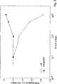
Es wurde in der – wie oben beschrieben – hergestellten Si-Schicht eine Stickstoffkonzentration über die Dicke von etwa 1 bis 4·1016 cm–3 gemessen, wie in
Eine mit dem Verfahren hergestellte Si-Schicht wird nun in einer kristallinen Si-Dünnschicht-Solarzelle eingesetzt, wie sie beispielsweise in Thin Solid Films 516 (2008) 6989–6993 beschrieben ist. Der Wirkungsgrad einer deratigen Solarzelle wurde gemessen.An Si layer produced by the method is now used in a crystalline Si thin-film solar cell, as described, for example, in Thin Solid Films 516 (2008) 6989-6993. The efficiency of a deratigen solar cell was measured.
Claims (8)
Translated fromGermanPriority Applications (1)
| Application Number | Priority Date | Filing Date | Title |
|---|---|---|---|
| DE102009056162.5ADE102009056162B4 (en) | 2009-11-27 | 2009-11-27 | Method for producing a low-defect crystalline silicon layer on a substrate by means of chemical or physical vapor deposition |
Applications Claiming Priority (1)
| Application Number | Priority Date | Filing Date | Title |
|---|---|---|---|
| DE102009056162.5ADE102009056162B4 (en) | 2009-11-27 | 2009-11-27 | Method for producing a low-defect crystalline silicon layer on a substrate by means of chemical or physical vapor deposition |
Publications (2)
| Publication Number | Publication Date |
|---|---|
| DE102009056162A1 DE102009056162A1 (en) | 2011-09-15 |
| DE102009056162B4true DE102009056162B4 (en) | 2015-12-24 |
Family
ID=44507639
Family Applications (1)
| Application Number | Title | Priority Date | Filing Date |
|---|---|---|---|
| DE102009056162.5AExpired - Fee RelatedDE102009056162B4 (en) | 2009-11-27 | 2009-11-27 | Method for producing a low-defect crystalline silicon layer on a substrate by means of chemical or physical vapor deposition |
Country Status (1)
| Country | Link |
|---|---|
| DE (1) | DE102009056162B4 (en) |
Citations (3)
| Publication number | Priority date | Publication date | Assignee | Title |
|---|---|---|---|---|
| US4670293A (en)* | 1983-07-29 | 1987-06-02 | Sanyo Electric Co., Ltd. | Method of making semiconductor film |
| EP1179620A1 (en)* | 2000-08-10 | 2002-02-13 | Hoya Corporation | Silicon carbide and method of manufacturing the same |
| WO2009128522A1 (en)* | 2008-04-18 | 2009-10-22 | Semiconductor Energy Laboratory Co., Ltd. | Thin film transistor and method for manufacturing the same |
Family Cites Families (1)
| Publication number | Priority date | Publication date | Assignee | Title |
|---|---|---|---|---|
| CN101436107B (en)* | 2007-11-15 | 2010-12-29 | 深圳富泰宏精密工业有限公司 | Writing pencil |
- 2009
- 2009-11-27DEDE102009056162.5Apatent/DE102009056162B4/ennot_activeExpired - Fee Related
Patent Citations (3)
| Publication number | Priority date | Publication date | Assignee | Title |
|---|---|---|---|---|
| US4670293A (en)* | 1983-07-29 | 1987-06-02 | Sanyo Electric Co., Ltd. | Method of making semiconductor film |
| EP1179620A1 (en)* | 2000-08-10 | 2002-02-13 | Hoya Corporation | Silicon carbide and method of manufacturing the same |
| WO2009128522A1 (en)* | 2008-04-18 | 2009-10-22 | Semiconductor Energy Laboratory Co., Ltd. | Thin film transistor and method for manufacturing the same |
Non-Patent Citations (6)
| Title |
|---|
| A. Karoui: Silicon Crystal Growth and Wafer Processing for High Efficiency Solar Cells and HighMechanical Yield. In: NREL/CP-520-31057, October 2001* |
| D.J. EAGLESHAM: Effect of H on Si molecular-beam epitaxy. In: J. Appl. Phys., 74 (11), Dezember 1992, S. 6615 - 6618* |
| J.R. ARTHUR: Molekular beam epitaxy. In: Surface Science, 500, 2002, S.189-217* |
| M. AKATSUKA: Pinning Effect on Punched-Out Dislocations in Carbon-, Nitrogen- or Boron-Doped Silicon Wafers, Vol. 40, 2001, S. 1240 - 1241* |
| P.DOGAN: Structural and electrical properties of epitaxial Si layers prepared by E-beam evaporation. In: Thin Solid Films, 516, 2008, S.6989-6993* |
| W.v. AMMON: Influence of ogygen and nitrogen on piont effect aggregation in silicon single crystals. In: Materials Science and Engeneering, B36, 1996, S.33-41* |
Also Published As
| Publication number | Publication date |
|---|---|
| DE102009056162A1 (en) | 2011-09-15 |
Similar Documents
| Publication | Publication Date | Title |
|---|---|---|
| DE102009022224B4 (en) | Process for producing epitaxial silicon wafers | |
| DE102014205466B4 (en) | Single crystal 4H-SiC substrate and process for its preparation | |
| DE10152707B4 (en) | Process for the production of a solar cell | |
| DE3415799A1 (en) | METHOD FOR PRODUCING A SINGLE-CRYSTAL SUBSTRATE FROM SILICON CARBIDE | |
| EP2815004B1 (en) | Method for producing iii-n single crystals, and iii-n single crystal | |
| DE102009004557B4 (en) | Epitaxial silicon wafer and process for producing epitaxially coated silicon wafers | |
| DE602005004280T2 (en) | METHOD FOR THE PULLING OF SIC-EINCROISTALLEN AND SIC-EINKRISTALL | |
| DE112009000328B4 (en) | Process for growing a silicon carbide single crystal | |
| DE102008022747B4 (en) | Silicon single crystal wafers and method of manufacture | |
| DE112019004549T5 (en) | Process for the effective elimination of graphene wrinkles by chemical vapor deposition (CVD) | |
| DE102018213437B4 (en) | Method of making gallium nitride substrate using hydride gas phase epitaxy | |
| DE4138121A1 (en) | SOLAR CELL AND METHOD FOR THE PRODUCTION THEREOF | |
| DE60125472T3 (en) | SiC material and process for its preparation | |
| DE112018002163T5 (en) | A method of manufacturing a silicon single crystal, a method of manufacturing an epitaxial silicon wafer, a silicon single crystal, and an epitaxial silicon wafer | |
| EP3662504A1 (en) | Semiconductor wafer made of monocrystalline silicon and method for producing the semiconductor wafer | |
| DE3751884T2 (en) | Method of manufacturing a deposited crystal layer | |
| DE102009056162B4 (en) | Method for producing a low-defect crystalline silicon layer on a substrate by means of chemical or physical vapor deposition | |
| DE68901735T2 (en) | METHOD FOR PRODUCING SEMI-CONDUCTING CRYSTALS. | |
| DE102015115961B4 (en) | Process for the production of a monocrystalline SiC wafer | |
| DE102015218218B4 (en) | Method for producing a bonded SiC wafer | |
| Yu et al. | The growth of GeSn layer on patterned Si substrate by MBE method | |
| Uesugi et al. | MOVPE growth of InGaAsN films on Ge (001) on‐axis and vicinal substrates | |
| Milanova et al. | Effect of growth temperature on nitrogen incorporation into GaAsN during liquid-phase epitaxy | |
| DE102020132900B4 (en) | Silicon-based wafers and methods for producing silicon-based wafers | |
| DE102009001379B4 (en) | Semiconductor composite epitaxial wafers and their method of manufacture |
Legal Events
| Date | Code | Title | Description |
|---|---|---|---|
| R016 | Response to examination communication | ||
| R018 | Grant decision by examination section/examining division | ||
| R020 | Patent grant now final | ||
| R084 | Declaration of willingness to licence | ||
| R119 | Application deemed withdrawn, or ip right lapsed, due to non-payment of renewal fee |