DE102009038633B4 - Photoactive component with organic double or multiple mixed layers - Google Patents
Photoactive component with organic double or multiple mixed layersDownload PDFInfo
- Publication number
- DE102009038633B4 DE102009038633B4DE102009038633.5ADE102009038633ADE102009038633B4DE 102009038633 B4DE102009038633 B4DE 102009038633B4DE 102009038633 ADE102009038633 ADE 102009038633ADE 102009038633 B4DE102009038633 B4DE 102009038633B4
- Authority
- DE
- Germany
- Prior art keywords
- mixed
- layers
- absorber
- photoactive component
- photoactive
- Prior art date
- Legal status (The legal status is an assumption and is not a legal conclusion. Google has not performed a legal analysis and makes no representation as to the accuracy of the status listed.)
- Active
Links
- 239000000463materialSubstances0.000claimsabstractdescription87
- 239000006096absorbing agentSubstances0.000claimsabstractdescription38
- 239000011368organic materialSubstances0.000claimsabstractdescription13
- 238000001704evaporationMethods0.000claimsabstractdescription3
- 230000008020evaporationEffects0.000claimsabstractdescription3
- 239000010410layerSubstances0.000claimsdescription161
- 238000010521absorption reactionMethods0.000claimsdescription12
- 239000000758substrateSubstances0.000claimsdescription11
- XMWRBQBLMFGWIX-UHFFFAOYSA-NC60 fullereneChemical classC12=C3C(C4=C56)=C7C8=C5C5=C9C%10=C6C6=C4C1=C1C4=C6C6=C%10C%10=C9C9=C%11C5=C8C5=C8C7=C3C3=C7C2=C1C1=C2C4=C6C4=C%10C6=C9C9=C%11C5=C5C8=C3C3=C7C1=C1C2=C4C6=C2C9=C5C3=C12XMWRBQBLMFGWIX-UHFFFAOYSA-N0.000claimsdescription10
- 230000003595spectral effectEffects0.000claimsdescription9
- 230000003287optical effectEffects0.000claimsdescription8
- 239000012044organic layerSubstances0.000claimsdescription7
- 238000000862absorption spectrumMethods0.000claimsdescription6
- 238000009826distributionMethods0.000claimsdescription6
- 238000004768lowest unoccupied molecular orbitalMethods0.000claimsdescription6
- 230000005684electric fieldEffects0.000claimsdescription5
- 229910052751metalInorganic materials0.000claimsdescription5
- 239000002184metalSubstances0.000claimsdescription5
- 239000000203mixtureSubstances0.000claimsdescription5
- 150000003384small moleculesChemical class0.000claimsdescription5
- 229910003472fullereneInorganic materials0.000claimsdescription4
- 229920001940conductive polymerPolymers0.000claimsdescription3
- 229920000767polyanilinePolymers0.000claimsdescription3
- 229920000144PEDOT:PSSPolymers0.000claimsdescription2
- 125000002080perylenyl groupChemical classC1(=CC=C2C=CC=C3C4=CC=CC5=CC=CC(C1=C23)=C45)*0.000claimsdescription2
- 238000004770highest occupied molecular orbitalMethods0.000claims1
- 239000002800charge carrierSubstances0.000description9
- 229920000642polymerPolymers0.000description4
- 238000009792diffusion processMethods0.000description3
- 230000005525hole transportEffects0.000description3
- 239000011248coating agentSubstances0.000description2
- 238000000576coating methodMethods0.000description2
- 230000000295complement effectEffects0.000description2
- 230000031700light absorptionEffects0.000description2
- 238000004519manufacturing processMethods0.000description2
- 239000004065semiconductorSubstances0.000description2
- 238000000926separation methodMethods0.000description2
- 239000000243solutionSubstances0.000description2
- JBRZTFJDHDCESZ-UHFFFAOYSA-NAsGaChemical compound[As]#[Ga]JBRZTFJDHDCESZ-UHFFFAOYSA-N0.000description1
- 229910001218Gallium arsenideInorganic materials0.000description1
- 238000013459approachMethods0.000description1
- 229920001400block copolymerPolymers0.000description1
- 238000006243chemical reactionMethods0.000description1
- 238000010276constructionMethods0.000description1
- 239000013078crystalSubstances0.000description1
- 239000002019doping agentSubstances0.000description1
- 230000005284excitationEffects0.000description1
- 239000003574free electronSubstances0.000description1
- 239000011521glassSubstances0.000description1
- PCHJSUWPFVWCPO-UHFFFAOYSA-NgoldChemical compound[Au]PCHJSUWPFVWCPO-UHFFFAOYSA-N0.000description1
- 239000010931goldSubstances0.000description1
- 229910052737goldInorganic materials0.000description1
- 238000003306harvestingMethods0.000description1
- 238000010348incorporationMethods0.000description1
- 238000002347injectionMethods0.000description1
- 239000007924injectionSubstances0.000description1
- 238000000034methodMethods0.000description1
- 230000007935neutral effectEffects0.000description1
- 238000005457optimizationMethods0.000description1
- 230000005693optoelectronicsEffects0.000description1
- 230000035515penetrationEffects0.000description1
- 238000005325percolationMethods0.000description1
- 230000000737periodic effectEffects0.000description1
- 230000001443photoexcitationEffects0.000description1
- 239000002985plastic filmSubstances0.000description1
- 229920006255plastic filmPolymers0.000description1
- 238000005215recombinationMethods0.000description1
- 229910052710siliconInorganic materials0.000description1
- 239000010703siliconSubstances0.000description1
- 239000002356single layerSubstances0.000description1
- 239000007787solidSubstances0.000description1
- 239000007790solid phaseSubstances0.000description1
- 239000002904solventSubstances0.000description1
- 238000001228spectrumMethods0.000description1
- 239000000126substanceSubstances0.000description1
- 239000010409thin filmSubstances0.000description1
- 230000007704transitionEffects0.000description1
- 239000012780transparent materialSubstances0.000description1
Images


Classifications
- B—PERFORMING OPERATIONS; TRANSPORTING
- B82—NANOTECHNOLOGY
- B82Y—SPECIFIC USES OR APPLICATIONS OF NANOSTRUCTURES; MEASUREMENT OR ANALYSIS OF NANOSTRUCTURES; MANUFACTURE OR TREATMENT OF NANOSTRUCTURES
- B82Y10/00—Nanotechnology for information processing, storage or transmission, e.g. quantum computing or single electron logic
- H—ELECTRICITY
- H10—SEMICONDUCTOR DEVICES; ELECTRIC SOLID-STATE DEVICES NOT OTHERWISE PROVIDED FOR
- H10K—ORGANIC ELECTRIC SOLID-STATE DEVICES
- H10K30/00—Organic devices sensitive to infrared radiation, light, electromagnetic radiation of shorter wavelength or corpuscular radiation
- H10K30/20—Organic devices sensitive to infrared radiation, light, electromagnetic radiation of shorter wavelength or corpuscular radiation comprising organic-organic junctions, e.g. donor-acceptor junctions
- H10K30/211—Organic devices sensitive to infrared radiation, light, electromagnetic radiation of shorter wavelength or corpuscular radiation comprising organic-organic junctions, e.g. donor-acceptor junctions comprising multiple junctions, e.g. double heterojunctions
- H—ELECTRICITY
- H10—SEMICONDUCTOR DEVICES; ELECTRIC SOLID-STATE DEVICES NOT OTHERWISE PROVIDED FOR
- H10K—ORGANIC ELECTRIC SOLID-STATE DEVICES
- H10K30/00—Organic devices sensitive to infrared radiation, light, electromagnetic radiation of shorter wavelength or corpuscular radiation
- H10K30/30—Organic devices sensitive to infrared radiation, light, electromagnetic radiation of shorter wavelength or corpuscular radiation comprising bulk heterojunctions, e.g. interpenetrating networks of donor and acceptor material domains
- H—ELECTRICITY
- H10—SEMICONDUCTOR DEVICES; ELECTRIC SOLID-STATE DEVICES NOT OTHERWISE PROVIDED FOR
- H10K—ORGANIC ELECTRIC SOLID-STATE DEVICES
- H10K30/00—Organic devices sensitive to infrared radiation, light, electromagnetic radiation of shorter wavelength or corpuscular radiation
- H10K30/40—Organic devices sensitive to infrared radiation, light, electromagnetic radiation of shorter wavelength or corpuscular radiation comprising a p-i-n structure, e.g. having a perovskite absorber between p-type and n-type charge transport layers
- H—ELECTRICITY
- H10—SEMICONDUCTOR DEVICES; ELECTRIC SOLID-STATE DEVICES NOT OTHERWISE PROVIDED FOR
- H10K—ORGANIC ELECTRIC SOLID-STATE DEVICES
- H10K30/00—Organic devices sensitive to infrared radiation, light, electromagnetic radiation of shorter wavelength or corpuscular radiation
- H10K30/50—Photovoltaic [PV] devices
- H10K30/57—Photovoltaic [PV] devices comprising multiple junctions, e.g. tandem PV cells
- H—ELECTRICITY
- H10—SEMICONDUCTOR DEVICES; ELECTRIC SOLID-STATE DEVICES NOT OTHERWISE PROVIDED FOR
- H10K—ORGANIC ELECTRIC SOLID-STATE DEVICES
- H10K85/00—Organic materials used in the body or electrodes of devices covered by this subclass
- H10K85/20—Carbon compounds, e.g. carbon nanotubes or fullerenes
- H10K85/211—Fullerenes, e.g. C60
- H—ELECTRICITY
- H10—SEMICONDUCTOR DEVICES; ELECTRIC SOLID-STATE DEVICES NOT OTHERWISE PROVIDED FOR
- H10K—ORGANIC ELECTRIC SOLID-STATE DEVICES
- H10K85/00—Organic materials used in the body or electrodes of devices covered by this subclass
- H10K85/60—Organic compounds having low molecular weight
- H10K85/631—Amine compounds having at least two aryl rest on at least one amine-nitrogen atom, e.g. triphenylamine
- H—ELECTRICITY
- H10—SEMICONDUCTOR DEVICES; ELECTRIC SOLID-STATE DEVICES NOT OTHERWISE PROVIDED FOR
- H10K—ORGANIC ELECTRIC SOLID-STATE DEVICES
- H10K85/00—Organic materials used in the body or electrodes of devices covered by this subclass
- H10K85/60—Organic compounds having low molecular weight
- H10K85/649—Aromatic compounds comprising a hetero atom
- H10K85/655—Aromatic compounds comprising a hetero atom comprising only sulfur as heteroatom
- Y—GENERAL TAGGING OF NEW TECHNOLOGICAL DEVELOPMENTS; GENERAL TAGGING OF CROSS-SECTIONAL TECHNOLOGIES SPANNING OVER SEVERAL SECTIONS OF THE IPC; TECHNICAL SUBJECTS COVERED BY FORMER USPC CROSS-REFERENCE ART COLLECTIONS [XRACs] AND DIGESTS
- Y02—TECHNOLOGIES OR APPLICATIONS FOR MITIGATION OR ADAPTATION AGAINST CLIMATE CHANGE
- Y02E—REDUCTION OF GREENHOUSE GAS [GHG] EMISSIONS, RELATED TO ENERGY GENERATION, TRANSMISSION OR DISTRIBUTION
- Y02E10/00—Energy generation through renewable energy sources
- Y02E10/50—Photovoltaic [PV] energy
- Y02E10/549—Organic PV cells
- Y—GENERAL TAGGING OF NEW TECHNOLOGICAL DEVELOPMENTS; GENERAL TAGGING OF CROSS-SECTIONAL TECHNOLOGIES SPANNING OVER SEVERAL SECTIONS OF THE IPC; TECHNICAL SUBJECTS COVERED BY FORMER USPC CROSS-REFERENCE ART COLLECTIONS [XRACs] AND DIGESTS
- Y02—TECHNOLOGIES OR APPLICATIONS FOR MITIGATION OR ADAPTATION AGAINST CLIMATE CHANGE
- Y02P—CLIMATE CHANGE MITIGATION TECHNOLOGIES IN THE PRODUCTION OR PROCESSING OF GOODS
- Y02P70/00—Climate change mitigation technologies in the production process for final industrial or consumer products
- Y02P70/50—Manufacturing or production processes characterised by the final manufactured product
Landscapes
- Engineering & Computer Science (AREA)
- Physics & Mathematics (AREA)
- Chemical & Material Sciences (AREA)
- Electromagnetism (AREA)
- Nanotechnology (AREA)
- Materials Engineering (AREA)
- Mathematical Physics (AREA)
- Theoretical Computer Science (AREA)
- Crystallography & Structural Chemistry (AREA)
- Photovoltaic Devices (AREA)
Abstract
Translated fromGerman
Description
Translated fromGermanDie Erfindung betrifft ein photoaktives Bauelement mit organischen Schichten, insbesondere eine Solarzelle nach dem Oberbegriff des Anspruchs 1.The invention relates to a photoactive component with organic layers, in particular a solar cell according to the preamble of
Seit der Demonstration der ersten organischen Solarzelle mit einem Wirkungsgrad im Prozentbereich durch
Organische Solarzellen bestehen aus einer Folge dünner Schichten (typischerweise 1 nm bis 1 µm) aus organischen Materialien, welche bevorzugt im Vakuum aufgedampft oder aus einer Lösung aufgeschleudert werden. Die elektrische Kontaktierung kann durch Metallschichten, transparente leitfähige Oxide (TCOs) und/oder transparente leitfähige Polymere (PEDOT-PSS, PANI) erfolgen.Organic solar cells consist of a sequence of thin layers (typically 1 nm to 1 μm) of organic materials, which are preferably vapor-deposited in vacuum or spin-coated from a solution. The electrical contacting can be effected by metal layers, transparent conductive oxides (TCOs) and / or transparent conductive polymers (PEDOT-PSS, PANI).
Eine Solarzelle wandelt Lichtenergie in elektrische Energie um. In diesem Sinne wird hier der Begriff „photoaktiv“ verstanden, nämlich der Umwandlung von Lichtenergie in elektrische Energie. Im Gegensatz zu anorganischen Solarzellen werden bei organischen Solarzellen durch das Licht nicht direkt freie Ladungsträger erzeugt, sondern es bilden sich zunächst Exzitonen, also elektrisch neutrale Anregungszustände (gebundene Elektron-Loch-Paare). Erst in einem zweiten Schritt werden diese Exzitonen in freie Ladungsträger getrennt, die dann zum elektrischen Stromfluß beitragen.A solar cell converts light energy into electrical energy. In this sense, the term "photoactive" is understood here, namely the conversion of light energy into electrical energy. In contrast to inorganic solar cells, solar cells do not directly generate free charge carriers by light, but excitons are first formed, ie electrically neutral excitation states (bound electron-hole pairs). Only in a second step, these excitons are separated into free charge carriers, which then contribute to the electric current flow.
Der Vorteil solcher Bauelemente auf organischer Basis gegenüber den konventionellen Bauelementen auf anorganischer Basis (Halbleiter wie Silizium, Galliumarsenid) sind die teilweise extrem hohen optischen Absorptionskoeffizienten (bis zu 2 × 105 cm-1), die es erlauben, effiziente Absorberschichten von nur wenigen Nanometern Dicke herzustellen, so dass sich die Möglichkeit bietet, mit geringem Material- und Energieaufwand sehr dünne Solarzellen herzustellen. Weitere technologische Aspekte sind die niedrigen Kosten, wobei die verwendeten organischen Halbleitermaterialien bei Herstellung in größeren Mengen sehr kostengünstig sind, die Möglichkeit, flexible großflächige Bauteile auf Plastikfolien herzustellen, die nahezu unbegrenzten Variationsmöglichkeiten und die unbegrenzte Verfügbarkeit der organischen Chemie.The advantage of such organic-based devices over conventional inorganic-based devices (semiconductors such as silicon, gallium arsenide) is the sometimes extremely high optical absorption coefficients (up to 2 × 105 cm-1 ) that allow efficient absorber layers of only a few nanometers Thickness produce, so that offers the opportunity to produce very thin solar cells with low material and energy costs. Further technological aspects are the low costs, with the organic semiconductor materials used being very cost-effective when produced in large quantities, the possibility of producing flexible large-area components on plastic films, the almost unlimited possibilities of variation and the unlimited availability of organic chemistry.
Eine in der Literatur bereits vorgeschlagene Realisierungsmöglichkeit einer organischen Solarzelle besteht in einer pin-Diode [Martin Pfeiffer, „Controlled doping of organic vacuum deposited dye layers: basics and applications“, PhD thesis TU-Dresden, 1999.] mit folgendem Schichtaufbau:
- 0. Träger, Substrat,
- 1. Grundkontakt, meist transparent,
- 2. p-Schicht(en),
- 3. i-Schicht(en),
- 4. n-Schicht(en),
- 5. Deckkontakt.
- 0. carrier, substrate,
- 1. basic contact, mostly transparent,
- 2nd p-layer (s),
- 3rd i-layer (s),
- 4th n-layer (s),
- 5. Deck contact.
Hierbei bedeutet n bzw. p eine n- bzw. p-Dotierung, die zu einer Erhöhung der Dichte freier Elektronen bzw. Löcher im thermischen Gleichgewichtszustand führt. In diesem Sinne sind derartige Schichten primär als Transportschichten zu verstehen. Die Bezeichnung i-Schicht bezeichnet demgegenüber eine undotierte Schicht (intrinsische Schicht). Eine oder mehrere i-Schicht(en) können hierbei Schichten sowohl aus einem Material, als auch eine Mischung aus zwei Materialien (sogenannte interpenetrierende Netzwerke) bestehen. Das durch den transparenten Grundkontakt einfallende Licht erzeugt in der i-Schicht bzw. in der n-/p-Schicht Exzitonen. Diese Exzitonen können nur durch sehr hohe elektrische Felder oder an geeigneten Grenzflächen getrennt werden. In organischen Solarzellen stehen ausreichend hohe Felder nicht zur Verfügung, so dass alle Erfolg versprechenden Konzepte für organische Solarzellen auf der Exzitonentrennung an photoaktiven Grenzflächen beruhen. Die Exzitonen gelangen durch Diffusion an eine derartige aktive Grenzfläche, wo Elektronen und Löcher voneinander getrennt werden. Diese kann zwischen der p- (n-)Schicht und der i-Schicht bzw. zwischen zwei i-Schichten liegen. Im eingebauten elektrischen Feld der Solarzelle werden die Elektronen nun zum n-Gebiet und die Löcher zum p-Gebiet abtransportiert. Vorzugsweise handelt es sich bei den Transportschichten um transparente oder weitgehend transparente Materialien mit großer Bandlücke (wide-gap). Als wide-gap Materialien werden hierbei Materialien bezeichnet, deren Absorptionsmaximum im Wellenlängenbereich < 450 nm liegt, bevorzugt bei < 400 nm.Here, n or p denotes an n- or p-type doping, which leads to an increase in the density of free electrons or holes in the thermal equilibrium state. In this sense, such layers are primarily to be understood as transport layers. In contrast, the term i-layer designates an undoped layer (intrinsic layer). One or more i-layer (s) may in this case consist of layers of a material as well as a mixture of two materials (so-called interpenetrating networks). The light incident through the transparent base contact generates excitons in the i-layer or in the n- / p-layer. These excitons can only be separated by very high electric fields or at suitable interfaces. In organic solar cells, sufficiently high fields are not available, so that all promising concepts for organic solar cells based on the exciton separation at photoactive interfaces. The excitons pass through diffusion to such an active interface, where electrons and holes are separated. This can lie between the p (n) layer and the i-layer or between two i-layers. In the built-in electric field of the solar cell, the electrons are now transported to the n-area and the holes to the p-area. Preferably, the transport layers are transparent or largely transparent materials with a wide band gap (wide-gap). As wide-gap materials in this case materials are referred to, the absorption maximum in the wavelength range <450 nm, preferably at <400 nm.
Da durch das Licht immer erst Exzitonen erzeugt werden und noch keine freien Ladungsträger, spielt die rekombinationsarme Diffusion von Exzitonen an die aktive Grenzfläche eine kritische Rolle bei organischen Solarzellen. Um einen Beitrag zum Photostrom zu leisten, muss daher in einer guten organischen Solarzelle die Exzitonendiffusionslänge die typische Eindringtiefe des Lichts deutlich übersteigen, damit der überwiegende Teil des Lichts genutzt werden kann. Strukturell und bezüglich der chemischen Reinheit perfekte organische Kristalle oder Dünnschichten erfüllen durchaus dieses Kriterium. Für großflächige Anwendungen ist allerdings die Verwendung von monokristallinen organischen Materialien nicht möglich und die Herstellung von Mehrfachschichten mit ausreichender struktureller Perfektion ist bis jetzt noch sehr schwierig.Since excitons are always generated by the light and no free charge carriers, the low-recombination diffusion of excitons to the active interface plays a critical role in organic solar cells. In order to make a contribution to the photocurrent, therefore, in a good organic solar cell, the exciton diffusion length must significantly exceed the typical penetration depth of the light, so that the greater part of the light can be used. Structurally and with regard to chemical purity, perfect organic crystals or thin films definitely fulfill this criterion. For large area applications, however, the use of monocrystalline organic materials is not possible and the production of multiple layers with sufficient structural perfection is still very difficult.
Falls es sich bei der i-Schicht um eine Mischschicht handelt, so übernimmt die Aufgabe der Lichtabsorption entweder nur eine der Komponenten oder auch beide. Der Vorteil von Mischschichten ist, dass die erzeugten Exzitonen nur einen sehr kurzen Weg zurücklegen müssen bis sie an eine Domänengrenze gelangen, wo sie getrennt werden. Der Abtransport der Elektronen bzw. Löcher erfolgt getrennt in den jeweiligen Materialien. Da in der Mischschicht die Materialien überall miteinander im Kontakt sind, ist bei diesem Konzept entscheidend, dass die getrennten Ladungen eine lange Lebensdauer auf dem jeweiligen Material besitzen und von jedem Ort aus geschlossene Perkolationspfade für beide Ladungsträgersorten zum jeweiligen Kontakt hin vorhanden sind. If the i-layer is a mixed layer, the task of absorbing light either takes on only one of the components or both. The advantage of mixed layers is that the generated excitons only travel a very short distance until they reach a domain boundary where they are separated. The removal of the electrons or holes is carried out separately in the respective materials. Since in the mixed layer the materials are in contact with each other everywhere, it is crucial in this concept that the separate charges have a long service life on the respective material and that there are closed percolation paths for each type of charge to the respective contact from each location.
Aus der Literatur sind verschiedene Realisierungsmöglichkeiten für die photoaktive i-Schicht bekannt: So kann es sich hierbei um eine Doppelschicht (
Weiterhin sind Tandem- bzw. Mehrfachsolarzellen aus der Literatur bekannt (Hiramoto, Chem. Lett., 1990, 327 (1990);
Das Problem von organischen Solarzellen besteht darin, dass aus elektrischen Gründen (nur eingeschränkt guter Transport für die Ladungsträger) die i-Schicht(en) nur sehr dünn gemacht werden kann (können). Dies hat zur Folge, dass nur ein Teil des Lichts im Bauelement absorbiert wird. Weiterhin sind die Absorptionsbanden von organischen Materialien begrenzt breit und haben für die meisten effizienten in Solarzellen eingesetzten Materialien typischerweise eine spektrale Breite von ca. 200 nm. Dies hat zur Folge, dass die beiden Materialien, die den photoaktiven Übergang bilden (Doppelschicht oder Mischschicht) nur einen spektralen Bereich von ca. 400 nm abdecken können. Eine Solarzelle mit einem sehr hohen Wirkungsgrad muss aber möglichst über den kompletten Spektralbereich von ca. 350 nm bis ca. 1000 nm über eine sehr hohe Absorption verfügen.The problem with organic solar cells is that, for electrical reasons (limited transportability for the charge carriers), the i-layer (s) can only be made very thin. As a result, only part of the light is absorbed in the device. Furthermore, the absorption bands of organic materials are limited in width and typically have a spectral width of about 200 nm for most efficient materials used in solar cells. As a result, the two materials that form the photoactive transition (bilayer or mixed layer) only can cover a spectral range of about 400 nm. However, a solar cell with a very high efficiency must have a very high absorption over the entire spectral range of about 350 nm to about 1000 nm.
Der Erfindung liegt somit die Aufgabe zugrunde, dass die photoaktiven Schichten des Bauelementes möglichst viel Licht absorbieren sollen. Insbesondere soll der Spektralbereich, in dem das Bauelement Licht absorbiert, möglichst breit gestaltet werden können.The invention is thus based on the object that the photoactive layers of the device should absorb as much light as possible. In particular, the spectral range in which the component absorbs light should be as wide as possible.
Die Aufgabe wird durch ein photoaktives Bauelement gemäß dem Hauptanspruch gelöst. Vorteilhafte Ausgestaltungen sind in den Unteransprüchen angegeben.The object is achieved by a photoactive component according to the main claim. Advantageous embodiments are specified in the subclaims.
Erfindungsgemäß besteht das i-Schichtsystem des photoaktiven Bauelementes mindestens aus zwei Mischschichten, die direkt aneinandergrenzen und mindestens eine der beiden Hauptmaterialien einer Mischschicht ein anderes organisches Material ist als die beiden Hauptmaterialien einer anderen Mischschicht. Jede Mischschicht besteht aus mindestens zwei Hauptmaterialien, wobei diese ein photoaktives Donor-Akzeptor-System bilden. Das Donor-Akzeptor-System zeichnet sich dadurch aus, dass zumindest für die Photoanregung der Donor-Komponente gilt, dass die gebildeten Exzitonen an der Grenzfläche zum Akzeptor bevorzugt in ein Loch auf dem Donor und ein Elektron auf dem Akzeptor getrennt werden. Als Hauptmaterial wird ein Material bezeichnet, dessen Volumen- oder Massen-Anteil in der Schicht größer als 16% ist. Weitere Materialien können technisch bedingt oder aber zur Einstellung von Schichteigenschaften beigemischt sein.According to the invention, the i-layer system of the photoactive component consists of at least two mixed layers which adjoin one another directly and at least one of the two main materials of a mixed layer is an organic material other than the two main materials of another mixed layer. Each mixed layer consists of at least two main materials forming a photoactive donor-acceptor system. The donor-acceptor system is characterized in that, at least for the photoexcitation of the donor component, the excitons formed at the interface to the acceptor are preferably separated into a hole on the donor and an electron on the acceptor. The main material is a material whose volume or mass fraction in the layer is greater than 16%. Other materials can be mixed for technical reasons or to adjust layer properties.
Solch ein Bauelement ist noch nicht aus Veröffentlichungen bekannt. Bereits bei einer Doppelmischschicht enthält das Bauelement drei bzw. vier verschiedene Absorbermaterialien, kann damit einen Spektralbereich von ca. 600 nm bzw. ca. 800 nm abdecken und somit die gestellte Aufgabe erfüllen.Such a device is not yet known from publications. Already in the case of a double-mixed layer, the component contains three or four different absorber materials, so that it can cover a spectral range of approximately 600 nm or approximately 800 nm and thus fulfill the stated task.
In einer weiteren Ausführung der Erfindung kann die Doppelmischschicht auch dazu benutzt werden, für einen bestimmten Spektralbereich deutlich höhere Photoströme zu erzielen, indem Materialien gemischt werden, die bevorzugt in demselben Spektralbereich absorbieren. Dies kann dann im Weiteren benutzt werden, um in einer Tandemsolarzelle oder Mehrfachsolarzelle eine Stromanpassung zwischen den verschiedenen Teilzellen zu erreichen. In a further embodiment of the invention, the double-mixed layer can also be used to achieve significantly higher photocurrents for a specific spectral range by mixing materials which preferentially absorb in the same spectral range. This can then be used subsequently to achieve a current matching between the various subcells in a tandem solar cell or multiple solar cell.
In einer weiteren Ausführungsform der Erfindung können zur Verbesserung der Ladungsträgertransporteigenschaften der Mischschichten die Mischungsverhältnisse in den verschiedenen Mischschichten gleich oder auch unterschiedlich sein.In a further embodiment of the invention, in order to improve the charge carrier transport properties of the mixed layers, the mixing ratios in the different mixed layers may be the same or different.
In einer weiteren Ausführungsform der Erfindung bestehen die Mischschichten bevorzugt aus jeweils zwei Hauptmaterialien.In a further embodiment of the invention, the mixed layers preferably consist of two main materials each.
In einer weiteren Ausführungsform der Erfindung kann in den einzelnen Mischschichten ein Gradient des Mischungsverhältnisses vorhanden sein.In a further embodiment of the invention, a gradient of the mixing ratio may be present in the individual mixed layers.
In einer weiteren Ausführungsform der Erfindung ist das Bauelement als organische pin-Solarzelle bzw. organische pin-Tandemsolarzelle ausgeführt. Als Tandemsolarzelle wird dabei eine Solarzelle bezeichnet, die aus einem vertikalen Stapel zweier in Serie verschalteter Solarzellen besteht.In a further embodiment of the invention, the component is designed as an organic pin solar cell or organic pin tandem solar cell. As a tandem solar cell while a solar cell is referred to, which consists of a vertical stack of two series-connected solar cells.
In einer bevorzugten Ausgestaltung der Erfindung ist das photoaktive Bauelement als Tandemzellen ausgeführt und es besteht durch die Verwendung von Doppel- bzw. Mehrfachmischschichten der weitere Vorteil, dass die Strom-Angleichung (current matching) zwischen den Teilzellen durch die Wahl der Absorbermaterialien in den Mischschichten optimiert und damit der Wirkungsgrad weiter erhöht werden kann.In a preferred embodiment of the invention, the photoactive component is designed as tandem cells and there is the further advantage through the use of double or multiple mixed layers, that the current matching between the sub-cells optimized by the choice of absorber materials in the mixed layers and thus the efficiency can be further increased.
In einer weiteren Ausführungsform der Erfindung können die einzelnen Materialien dabei in unterschiedlichen Maxima der Lichtverteilung der charakteristischen Wellenlängen, die dieses Material absorbiert, positioniert sein. So kann beispielsweise ein Material in einer Mischschicht im 2. Maximum seiner charakteristischen Wellenlänge liegen und das andere Material im 3. Maximum.In a further embodiment of the invention, the individual materials may be positioned in different maxima of the light distribution of the characteristic wavelengths which this material absorbs. For example, one material in a mixed layer may be in the 2nd maximum of its characteristic wavelength and the other material in the 3rd maximum.
In einer weiteren Ausführungsform der Erfindung besteht das photoaktive Bauelement, insbesondere eine organische Solarzelle, aus einer Elektrode und einer Gegenelektrode und zwischen den Elektroden wenigstens zwei organischen photoaktiven Mischschichten, wobei die Mischschichten jeweils im wesentlichen aus zwei Materialien bestehen und die beiden Hauptmaterialien jeweils einer Mischschicht ein Donator-Akzeptor-System bilden sowie die beiden Mischschichten direkt aneinandergrenzen und wenigstens eine der beiden Hauptmaterialien der einen Mischschicht ein anderes organisches Material ist als die beiden Hauptmaterialien einer anderen Mischschicht.In a further embodiment of the invention, the photoactive component, in particular an organic solar cell, consists of an electrode and a counterelectrode and at least two organic photoactive mixed layers between the electrodes, the mixed layers each consisting essentially of two materials and the two main materials each of a mixed layer Form donor-acceptor system and the two mixed layers directly adjacent to each other and at least one of the two main materials of a mixed layer is a different organic material than the two main materials of another mixed layer.
In einer Weiterbildung der vorbeschriebenen Ausführungsform sind mehrere oder alle Hauptmaterialien der Mischschichten voneinander verschieden.In a development of the above-described embodiment, several or all of the main materials of the mixed layers are different from one another.
In einer weiteren Ausführungsform der Erfindung handelt es sich um drei oder mehr Mischschichten, welche zwischen der Elektrode und Gegenelektrode angeordnet sind.In a further embodiment of the invention, there are three or more mixed layers, which are arranged between the electrode and counter electrode.
In einer weiteren Ausführungsform der Erfindung sind zusätzlich zu den genannten Mischschichten noch weitere photoaktive Einzel- oder Mischschichten vorhanden.In a further embodiment of the invention, further photoactive single or mixed layers are present in addition to the said mixed layers.
In einer weiteren Ausführungsform der Erfindung ist zwischen dem Mischschichtsystem und der einen Elektrode noch wenigstens eine weitere organische Schicht vorhanden.In a further embodiment of the invention, at least one further organic layer is present between the mixed-layer system and the one electrode.
In einer weiteren Ausführungsform der Erfindung ist zwischen dem Mischschichtsystem und der Gegenelektrode noch wenigstens eine weitere organische Schicht vorhanden.In a further embodiment of the invention, at least one further organic layer is present between the mixed-layer system and the counterelectrode.
In einer weiteren Ausführungsform der Erfindung sind eine oder mehrere der weiteren organischen Schichten dotierte wide-gap Schichten, wobei das Maximum der Absorption bei < 450 nm liegt.In a further embodiment of the invention, one or more of the further organic layers are doped wide-gap layers, wherein the maximum of the absorption is <450 nm.
In einer weiteren Ausführungsform der Erfindung beinhaltet das Bauelement eine pi-, ni-, ip-, in-, pin- oder nip-Struktur.In a further embodiment of the invention, the component includes a pi, ni, ip, in, pin or nip structure.
In einer weiteren Ausführungsform der Erfindung wird durch Verwendung von Lichtfallen der optische Weg des einfallenden Lichtes im aktiven System vergrößert.In a further embodiment of the invention, by using light traps, the optical path of the incident light in the active system is increased.
In einer weiteren Ausführungsform der Erfindung wird die Lichtfalle dadurch realisiert, dass das Bauelement auf einem periodisch mikrostrukturierten Substrat aufgebaut wird und die homogene Funktion des Bauelementes, dessen kurzschlussfreie Kontaktierung und eine homogene Verteilung des elektrischen Feldes über die gesamte Fläche durch die Verwendung einer dotierten wide-gap-Schicht gewährleistet wird. Besonders vorteilhaft ist dabei, dass das Licht die Absorberschicht mindestens zweimal durchläuft, was zu einer erhöhten Lichtabsorption und dadurch zu einem verbesserten Wirkungsgrad der Solarzelle führen kann. Dies lässt sich beispielsweise dadurch erreichen, dass das Substrat pyramidenartige Strukturen auf der Oberfläche aufweist mit Höhen (h) und Breiten (d) jeweils im Bereich von einem bis zu mehreren hundert Mikrometern. Höhe und Breite können gleich oder unterschiedlich gewählt werden. Ebenfalls können die Pyramiden symmetrisch oder asymmetrisch aufgebaut sein.In a further embodiment of the invention, the light trap is realized by constructing the device on a periodically microstructured substrate, and the homogeneous function of the device, its short-circuit free contacting and a homogeneous distribution of the electric field over the entire surface through the use of a doped wide- gap layer is ensured. It is particularly advantageous that the light passes through the absorber layer at least twice, which can lead to increased light absorption and thereby to improved efficiency of the solar cell. This can be achieved, for example, by the substrate having pyramid-like structures on the surface with heights (h) and widths (d) in the range from one to several hundred micrometers in each case. Height and width can be chosen the same or different. Likewise, the pyramids can be constructed symmetrically or asymmetrically.
In einer weiteren Ausführungsform der Erfindung wird die Lichtfalle dadurch realisiert, dass eine dotierte wide-gap-Schicht eine glatte Grenzfläche zur i-Schicht und eine rauhe Grenzfläche zum reflektierenden Kontakt hat. Die rauhe Grenzfläche kann beispielsweise durch eine periodische Mikrostrukturierung erreicht werden. Besonders vorteilhaft ist die rauhe Grenzfläche, wenn sie das Licht diffus. reflektiert, was zu einer Verlängerung des Lichtweges innerhalb der photoaktiven Schicht führt.In a further embodiment of the invention, the light trap is realized by having a doped wide-gap layer having a smooth interface with the i-layer and a rough interface with the reflective contact. The rough interface can be achieved for example by a periodic microstructuring. Particularly advantageous is the rough interface when they diffuse the light. reflected, which leads to an extension of the light path within the photoactive layer.
In einer weiteren Ausführungsform wird die Lichtfalle dadurch realisiert, dass das Bauelement auf einem periodisch mikrostrukturierten Substrat aufgebaut wird und eine dotierte wide-gap-Schicht eine glatte Grenzfläche zur i-Schicht und eine rauhe Grenzfläche zum reflektierenden Kontakt hat.In another embodiment, the light trap is realized by constructing the device on a periodically microstructured substrate and having a doped wide-gap layer having a smooth interface with the i-layer and a rough interface with the reflective contact.
In einer weiteren Ausführungsform der Erfindung weisen mindestens zwei Hauptmaterialien der Mischschichten verschiedene optische Absorptionsspektren auf.In a further embodiment of the invention, at least two main materials of the mixed layers have different optical absorption spectra.
In einer weiteren Ausführungsform der Erfindung weisen die Hauptmaterialien der Mischschichten verschiedene optische Absorptionsspektren auf, die sich gegenseitig ergänzen, um einen möglichst breiten Spektralbereich abzudecken.In a further embodiment of the invention, the main materials of the mixed layers have different optical absorption spectra, which complement each other to cover the widest possible spectral range.
In einer weiteren Ausführungsform der Erfindung erstreckt sich der Absorptionsbereich zumindest eines der Hauptmaterialien der Mischschichten in den Infrarot-Bereich.In a further embodiment of the invention, the absorption region of at least one of the main materials of the mixed layers extends into the infrared region.
In einer weiteren Ausführungsform der Erfindung erstreckt sich der Absorptionsbereich zumindest eines der Hauptmaterialien der Mischschichten in den Infrarot-Bereich im Wellenlängenbereich von > 700 nm bis 1500 nm.In a further embodiment of the invention, the absorption region of at least one of the main materials of the mixed layers extends into the infrared region in the wavelength range of> 700 nm to 1500 nm.
In einer weiteren Ausführungsform der Erfindung sind die HOMO- und LUMO-Niveaus der Hauptmaterialien so angepasst, dass das System eine maximale Leerlaufspannung, einen maximalen Kurzschlussstrom und einen maximalen Füllfaktor ermöglicht.In another embodiment of the invention, the HOMO and LUMO levels of the main materials are adjusted to allow the system to have a maximum open circuit voltage, a maximum short circuit current, and a maximum fill factor.
In einer weiteren Ausführungsform der Erfindung handelt es sich bei dem Bauelement um eine Tandem- oder Mehrfachstruktur.In a further embodiment of the invention, the component is a tandem or multiple structure.
In einer weiteren Ausführungsform der Erfindung handelt es sich bei den verwendeten organischen Materialien um kleine Moleküle. Unter kleinen Molekülen werden im Sinne der vorliegenden Erfindung nicht-polymere organische Moleküle mit monodispersen Molmassen zwischen 100 und 2000 verstanden, die unter Normaldruck (Luftdruck der uns umgebenden Atmosphäre) und bei Raumtemperatur in fester Phase vorliegen. Insbesondere können diese kleinen Moleküle auch photoaktiv sein, wobei unter photoaktiv verstanden wird, dass die Moleküle unter Lichteinfall ihren Ladungszustand ändern.In a further embodiment of the invention, the organic materials used are small molecules. For the purposes of the present invention, small molecules are understood as meaning non-polymeric organic molecules having monodisperse molecular weights between 100 and 2000, which are present under atmospheric pressure (atmospheric pressure of the atmosphere surrounding us) and in solid phase at room temperature. In particular, these small molecules can also be photoactive, which is understood to mean photoactively that the molecules change their charge state upon incidence of light.
In einer weiteren Ausführungsform der Erfindung handelt es sich bei den verwendeten organischen Materialien zumindest teilweise um Polymere.In a further embodiment of the invention, the organic materials used are at least partially polymers.
In einer weiteren Ausführungsform der Erfindung enthält mindestens eine der photoaktiven Mischschichten als Akzeptor ein Material aus der Gruppe der Fullerene bzw. Fullerenderivate (
In einer weiteren Ausführungsform der Erfindung enthalten alle photoaktiven Mischschichten als Akzeptor ein Material aus der Gruppe der Fullerene bzw. Fullerenderivate (
In einer weiteren Ausführungsform der Erfindung enthält mindestens eine der photoaktiven Mischschichten als Donator ein Material aus der Klasse der Phthalocyanine, Perylenderivate, TPD-Derivate, Oligothiophene oder ein Material wie es in
In einer weiteren Ausführungsform der Erfindung enthält mindestens eine der photoaktiven Mischschichten als Akzeptor das Material Fulleren
In einer weiteren Ausführungsform der Erfindung ist die Gesamtstruktur mit transparentem Grund- und Deckkontakt versehen.In a further embodiment of the invention, the entire structure is provided with a transparent base and cover contact.
In einer weiteren Ausführungsform der Erfindung bestehen die Kontakte aus Metall, einem leitfähigen Oxid, insbesondere ITO, ZnO:Al oder anderen TCOs oder einem leitfähigen Polymer, insbesondere PEDOT:PSS oder PANI.In a further embodiment of the invention, the contacts are made of metal, a conductive oxide, in particular ITO, ZnO: Al or other TCOs or a conductive polymer, in particular PEDOT: PSS or PANI.
Polymersolarzellen, die zwei oder mehrere photoaktive Mischschichten beinhalten, wobei die Mischschichten direkt aneinandergrenzen, sind nicht Bestandteil der Erfindung. Bei Polymersolarzellen besteht das Problem das die Materialien aus Lösung aufgebracht werden und somit eine weitere aufgebrachte Schicht sehr leicht dazu führt, dass die darunter liegenden Schichten angelöst, aufgelöst oder in ihrer Morphologie verändert werden. Bei Polymersolarzellen können daher nur sehr eingeschränkt Mehrfachmischschichten hergestellt werden und auch nur dadurch, dass verschiedene Material- und Lösungsmittelsysteme verwendet werden, die sich bei der Herstellung gegenseitig nicht oder kaum beeinflussen. Solarzellen aus kleinen Molekülen haben hier einen ganz klaren Vorteil, da durch den Aufdampfprozess im Vakuum beliebige Systeme und Schichten aufeinander gebracht werden können und somit der Vorteil der Mehrfachmischschichtstruktur sehr breit genutzt und mit beliebigen Materialkombinationen realisiert werden kann. Weiterhin ist der Einbau der Mehrfachmischschichten in pin-Strukturen (oder nip) mit kontrollierter n- und p-Dotierung sehr vorteilhaft. Unter kleinen Molekülen werden im Sinne der vorliegenden Erfindung nicht-polymere organische, photoaktive Moleküle verstanden.Polymer solar cells which contain two or more photoactive mixed layers, wherein the mixed layers are directly adjacent, are not part of the invention. Polymer solar cells have the problem that the materials are applied from solution and thus a further applied layer very easily causes the underlying layers to be dissolved, dissolved or changed in their morphology. In the case of polymer solar cells, therefore, only very limited multiple mixed layers can be produced and only in that different material and solvent systems are used, which do not influence one another or hardly influence each other during production. Small cell solar cells are here a very clear advantage, since the evaporation process in vacuum any systems and layers can be brought to each other and thus the advantage of the multiple mixed layer structure can be used very widely and can be realized with any combination of materials. Furthermore, the incorporation of the multiple mixed layers in pin structures (or nip) with controlled n and p doping is very advantageous. Within the meaning of the present invention, small molecules are understood as meaning non-polymeric organic, photoactive molecules.
In Mehrfachmischschichtsystemen treten vermehrt Transportprobleme für die Ladungsträger auf. Dieser Abtransport wird durch das eingebaute Feld der pin-Struktur deutlich erleichtert. Weiterhin können die Mehrfachmischschichten innerhalb einer pin-Struktur mit dotierten wide-gap Transportschichten verschoben werden, um eine optimale Absorption zu erzielen. Hierfür kann es auch sehr vorteilhaft sein, die pin-Struktur in eine nip-Struktur zu verändern. Speziell wenn die verschiedenen Materialien in den Mehrfachmischschichten in verschiedenen Wellenlängenbereichen absorbieren, können durch eine geeignete Wahl der Struktur (pin oder nip) bzw. eine geeignete Wahl der Schichtdicken der Transportschichten die verschiedenen Materialien jeweils an die optimale Position hinsichtlich der Intensitätsverteilung des Lichtes innerhalb des Bauelementes positioniert werden. Speziell bei Tandemzellen ist diese Optimierung sehr wichtig um einen Ausgleich der Photoströme der Einzelzellen zu erreichen und somit einen maximalen Wirkungsgrad zu erreichen.In multiple mixed-layer systems, transport problems increasingly occur for the charge carriers. This removal is greatly facilitated by the built-in field of the pin structure. Furthermore, the multiple mixed layers can be shifted within a pin structure with doped wide-gap transport layers in order to achieve optimum absorption. For this purpose, it can also be very advantageous to change the pin structure into a nip structure. Specifically, when the different materials in the multiple blend layers absorb in different wavelength ranges, by a suitable choice of structure (pin or nip) or a suitable choice of the layer thicknesses of the transport layers, the different materials can each reach the optimum position with respect to the intensity distribution of the light within the device be positioned. Especially with tandem cells, this optimization is very important to achieve a balance of the photocurrents of the individual cells and thus to achieve maximum efficiency.
Nachfolgend soll die Erfindung anhand einiger Ausführungsbeispiele und Figuren eingehend erläutert werden. Es zeigen
1 eine schematische Darstellung einer Struktur einer erfindungsgemäßen organischen Solarzelle,2 ein Energieniveau-Schema einer solchen Struktur,3 die Absorptionsspektren (k-Werte)der Materialien 4P-TPD, C60 und DCV6T4 die Strom-Spannungskennlinie von zwei erfindungsgemäßen organischen Solarzellen,5 dieStrukturformeln der Materialien 4P-TPD, C60 und DCV6T,6 die schematische Darstellung einer Struktur eines erfindungsgemäßen photoaktiven Bauelements auf mikrostrukturiertem Substrat, sowie7 die schematische Darstellung einer Struktur eines erfindungsgemäßen photoaktiven Bauelements auf mikrostrukturiertem Substrat.
1 a schematic representation of a structure of an organic solar cell according to the invention,2 an energy level scheme of such a structure,3 the absorption spectra (k-values) of thematerials 4P-TPD, C60 and DCV6T4 the current-voltage characteristic of two organic solar cells according to the invention,5 the structural formulas of thematerials 4P-TPD, C60 and DCV6T,6 the schematic representation of a structure of a photoactive device according to the invention on a microstructured substrate, and7 the schematic representation of a structure of a photoactive device according to the invention on a microstructured substrate.
Eine vorteilhafte Ausführung einer Struktur einer erfindungsgemäßen organischen Solarzelle beinhaltet folgende Schichten:
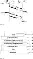
In
- HOMO (Höchstes besetztes Molekül-Orbital)
- LUMO (niedrigstes unbesetztes Molekül-Orbital)
- EF (Ferminiveau)
- p (Löchertransportschicht (HTL, hole transport layer))
- n (Elektronentransportschicht (ETL, electron transport layer))
- i1 (Mischschicht
1 ) - i2 (Mischschicht
2 )
In
- HOMO (Highest Occupied Molecule Orbital)
- LUMO (lowest unoccupied molecular orbital)
- EF (Fermi level)
- p (hole transport layer (HTL))
- n (electron transport layer (ETL))
- i1 (mixed layer
1 ) - i2 (mixed layer
2 )
Die in
- - durchgezogene Linien: Energieniveau des einen Hauptmaterials (Akzeptor
1 ) in i1 - - gestrichelte Linien: Energieniveau des anderen Hauptmaterials (Donator
1 ) in i1 - - gepunktete Linien: Energieniveau des einen Hauptmaterials (Akzeptor
2 ) in i2 - - langgestrichelte Linien: Energieniveau des anderen Hauptmaterials (Donator
2 ) in i2
- solid lines: energy level of the one main material (acceptor
1 ) in i1 - - dashed lines: energy level of the other main material (donator
1 ) in i1 - - dotted lines: energy level of the one main material (acceptor
2 ) in i2 - - long dashed lines: energy level of the other main material (donator
2 ) in i2
Vorzugsweise sind die HOMO und LUMO-Niveaus der verschiedenen Absorbermaterialien so angepasst, wie in
In einem weiteren Ausführungsbeispiel weist das erfindungsgemäße photoaktive Bauelement in
- 1.) Glas-
Substrat 1 , - 2.)
ITO Grundkontakt 2 , - 3.) Elektronentransportschicht (ETL)
3 , - 4.) aktives i-Doppel-
Schichtsystem 4P-TPD:C60/DCV6T:C60 - 5.) p-dotierte Löchertransportschicht (HTL)
6 , - 6.) Deckkontakt (z. B. Gold)
7 .
- 1.)
glass substrate 1 . - 2.)
ITO ground contact 2 . - 3.) Electron transport layer (ETL)
3 . - 4.) active i-double-
layer system 4P-TPD: C60 / DCV6T:C60 - 5.) p-doped hole transport layer (HTL)
6 . - 6.) cover contact (eg gold)
7 ,
In
Die
Die Solarzelle
Die
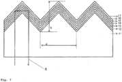
In einem weiteren Ausführungsbeispiel der Erfindung wird in
Dabei wird die Lichtfalle dadurch realisiert, dass das Bauelement auf einem periodisch mikrostrukturierten Substrat aufgebaut wird und die homogene Funktion des Bauelementes, dessen kurzschlussfreie Kontaktierung und eine homogene Verteilung des elektrischen Feldes über die gesamte Fläche durch die Verwendung einer dotierten wide-gap-Schicht gewährleistet wird. Besonders vorteilhaft ist dabei, dass das Licht die Absorberschicht mindestens zweimal durchläuft, was zu einer erhöhten Lichtabsorption und dadurch zu einem verbesserten Wirkungsgrad der Solarzelle führen kann. Dies lässt sich beispielsweise wie in
Das in
- 11:
- Substrat
- 12:
- Elektrode; z. B. ITO oder Metall (10-200 nm)
- 13:
- HTL oder ETL-Schichtsystem (10-200 nm)
- 14:
- Absorbermischschicht
1 (10-200 nm) - 15:
- Absorbermischschicht
2 (10-200 nm) - 16:
- HTL oder ETL-Schichtsystem (10-200 nm)
- 17:
- Elektrode; z. B. ITO oder Metall (10-200 nm)
- 11:
- substratum
- 12:
- Electrode; z. B. ITO or metal (10-200 nm)
- 13:
- HTL or ETL layer system (10-200 nm)
- 14:
- Absorber mixed layer
1 (10-200 nm) - 15:
- Absorber mixed layer
2 (10-200 nm) - 16:
- HTL or ETL layer system (10-200 nm)
- 17:
- Electrode; z. B. ITO or metal (10-200 nm)
BezugszeichenlisteLIST OF REFERENCE NUMBERS
- 11
- Träger, SubstratCarrier, substrate
- 22
- Grundkontakt (z. B. ITO)Basic contact (eg ITO)
- 33
- Ladungsträgertransportschicht (wide-gap), p- bzw. n-dotiertCharge carrier transport layer (wide-gap), p- or n-doped
- 44
- i2 (2. Mischschicht, 2. Absorbermischschicht)i2 (2nd mixed layer, 2nd mixed absorber layer)
- 55
- i1 (1. Mischschicht, 1. Absorber-Mischschicht)i1 (1st mixed layer, 1st mixed absorber layer)
- 66
- Ladungsträgertransportschicht (wide-gap), n- bzw. p-dotiertCharge carrier transport layer (wide-gap), n- or p-doped
- 77
- Deckkontaktdeck Contact
- 88th
- Weg des Lichts im BauelementPath of light in the component
- 1111
- Substratsubstratum
- 1212
- Elektrodeelectrode
- 1313
- HTL oder ETL-SchichtsystemHTL or ETL coating system
- 1414
- Absorbermischschicht
1 Absorbermixed layer 1 - 1515
- Absorbermischschicht
2 Absorbermixed layer 2 - 1616
- HTL oder ETL-SchichtsystemHTL or ETL coating system
- 1717
- Elektrodeelectrode
Claims (25)
Translated fromGermanPriority Applications (2)
| Application Number | Priority Date | Filing Date | Title |
|---|---|---|---|
| DE102009038633.5ADE102009038633B4 (en) | 2009-06-05 | 2009-08-26 | Photoactive component with organic double or multiple mixed layers |
| PCT/EP2010/057892WO2010139804A1 (en) | 2009-06-05 | 2010-06-07 | Photoactive component comprising double or multiple mixed layers |
Applications Claiming Priority (3)
| Application Number | Priority Date | Filing Date | Title |
|---|---|---|---|
| DE102009024295 | 2009-06-05 | ||
| DE102009024295.3 | 2009-06-05 | ||
| DE102009038633.5ADE102009038633B4 (en) | 2009-06-05 | 2009-08-26 | Photoactive component with organic double or multiple mixed layers |
Publications (2)
| Publication Number | Publication Date |
|---|---|
| DE102009038633A1 DE102009038633A1 (en) | 2010-12-16 |
| DE102009038633B4true DE102009038633B4 (en) | 2019-07-04 |
Family
ID=43069945
Family Applications (1)
| Application Number | Title | Priority Date | Filing Date |
|---|---|---|---|
| DE102009038633.5AActiveDE102009038633B4 (en) | 2009-06-05 | 2009-08-26 | Photoactive component with organic double or multiple mixed layers |
Country Status (2)
| Country | Link |
|---|---|
| DE (1) | DE102009038633B4 (en) |
| WO (1) | WO2010139804A1 (en) |
Families Citing this family (6)
| Publication number | Priority date | Publication date | Assignee | Title |
|---|---|---|---|---|
| DE102012106607B4 (en) | 2012-07-20 | 2024-04-04 | Heliatek Gmbh | Method for sealing modules with optoelectronic components |
| DE102012106815A1 (en) | 2012-07-26 | 2014-01-30 | Heliatek Gmbh | Method for contacting of optoelectronic components involves closing aperture in contact region according to electrical contact of electrical contact region and optoelectronic components |
| DE102013111164B4 (en) | 2013-10-09 | 2024-10-24 | Heliatek Gmbh | process for producing contact holes |
| DE112015004366A5 (en) | 2014-09-26 | 2017-06-08 | Heliatek Gmbh | PROCESS FOR APPLYING A PROTECTION LAYER, PROTECTION LAYER ITSELF AND SEMI-FINISHED MATERIAL WITH A PROTECTIVE LAYER |
| DE102020123252A1 (en) | 2019-12-12 | 2021-06-17 | Heliatek Gmbh | Coating for an optoelectronic component, method for producing such a coating, optoelectronic component with such a coating |
| DE102022100149A1 (en) | 2022-01-04 | 2023-07-06 | Heliatek Gmbh | Process for producing a photoactive layer in a layer system of an organic electronic component |
Citations (9)
| Publication number | Priority date | Publication date | Assignee | Title |
|---|---|---|---|---|
| EP0000829A1 (en) | 1977-08-02 | 1979-02-21 | EASTMAN KODAK COMPANY (a New Jersey corporation) | Photovoltaic elements |
| US5093698A (en) | 1991-02-12 | 1992-03-03 | Kabushiki Kaisha Toshiba | Organic electroluminescent device |
| DE19854938A1 (en) | 1998-11-27 | 2000-06-08 | Forschungszentrum Juelich Gmbh | Component used as a solar cell or LED, has layers separated by an interlayer containing one or both layer materials and a different conductivity material colloid |
| US6559375B1 (en) | 1998-11-27 | 2003-05-06 | Dieter Meissner | Organic solar cell or light-emitting diode |
| DE10209789A1 (en) | 2002-02-28 | 2003-09-25 | Univ Dresden Tech | Solar cell comprising organic, inorganic and mixed layers, the mixed layer being doped with strong acceptor or donor affecting only one main constituent |
| DE102004014046A1 (en) | 2003-03-19 | 2004-09-30 | Technische Universität Dresden | Photoactive device with organic layers |
| US20050110005A1 (en) | 2003-11-26 | 2005-05-26 | Forrest Stephen R. | Bipolar organic devices |
| DE102005010978A1 (en) | 2005-03-04 | 2006-09-07 | Technische Universität Dresden | Photoactive component with organic layers |
| DE102005010979A1 (en) | 2005-03-04 | 2006-09-21 | Technische Universität Dresden | Photoactive component with organic layers |
- 2009
- 2009-08-26DEDE102009038633.5Apatent/DE102009038633B4/enactiveActive
- 2010
- 2010-06-07WOPCT/EP2010/057892patent/WO2010139804A1/enactiveApplication Filing
Patent Citations (10)
| Publication number | Priority date | Publication date | Assignee | Title |
|---|---|---|---|---|
| EP0000829A1 (en) | 1977-08-02 | 1979-02-21 | EASTMAN KODAK COMPANY (a New Jersey corporation) | Photovoltaic elements |
| US5093698A (en) | 1991-02-12 | 1992-03-03 | Kabushiki Kaisha Toshiba | Organic electroluminescent device |
| DE19854938A1 (en) | 1998-11-27 | 2000-06-08 | Forschungszentrum Juelich Gmbh | Component used as a solar cell or LED, has layers separated by an interlayer containing one or both layer materials and a different conductivity material colloid |
| US6559375B1 (en) | 1998-11-27 | 2003-05-06 | Dieter Meissner | Organic solar cell or light-emitting diode |
| DE10209789A1 (en) | 2002-02-28 | 2003-09-25 | Univ Dresden Tech | Solar cell comprising organic, inorganic and mixed layers, the mixed layer being doped with strong acceptor or donor affecting only one main constituent |
| DE102004014046A1 (en) | 2003-03-19 | 2004-09-30 | Technische Universität Dresden | Photoactive device with organic layers |
| US20050110005A1 (en) | 2003-11-26 | 2005-05-26 | Forrest Stephen R. | Bipolar organic devices |
| DE102005010978A1 (en) | 2005-03-04 | 2006-09-07 | Technische Universität Dresden | Photoactive component with organic layers |
| WO2006092134A1 (en) | 2005-03-04 | 2006-09-08 | Heliatek Gmbh | Organic photoactive component |
| DE102005010979A1 (en) | 2005-03-04 | 2006-09-21 | Technische Universität Dresden | Photoactive component with organic layers |
Non-Patent Citations (1)
| Title |
|---|
| Tang et al. 1986 [C. W. Tang et al. Appl. Phys. Lett. 48, 183 (1986) |
Also Published As
| Publication number | Publication date |
|---|---|
| DE102009038633A1 (en) | 2010-12-16 |
| WO2010139804A1 (en) | 2010-12-09 |
Similar Documents
| Publication | Publication Date | Title |
|---|---|---|
| DE102004014046B4 (en) | Photoactive component with organic layers | |
| EP2398056B1 (en) | Organic solar cell with several transport layer systems | |
| EP2385556B1 (en) | Photoactive device with organic layers | |
| EP2513995B1 (en) | Photoactive component having organic layers | |
| DE102009051142B4 (en) | Photoactive component with inverted layer sequence and method for its production | |
| EP2400575B1 (en) | Optoelectronic construction element with organic layers | |
| EP2959520B1 (en) | Optoelectronic component | |
| DE10209789A1 (en) | Solar cell comprising organic, inorganic and mixed layers, the mixed layer being doped with strong acceptor or donor affecting only one main constituent | |
| WO2014206860A1 (en) | Organic semiconductive component | |
| DE102009038633B4 (en) | Photoactive component with organic double or multiple mixed layers | |
| WO2014006565A2 (en) | Transparent electrode for optoelectronic components | |
| WO2011064330A1 (en) | Organic photoactive component having cavity layer system | |
| WO2014006566A1 (en) | Electrode arrangement for optoelectronic components | |
| WO2021223814A1 (en) | Layer system for an organic electronic component | |
| DE102012105809B4 (en) | Organic optoelectronic component with transparent counterelectrode and transparent electrode device | |
| DE102012105810B4 (en) | Transparent electrode for optoelectronic components | |
| DE102012103448B4 (en) | Method of optimizing serially connected photoactive devices on curved surfaces | |
| DE102013110373B4 (en) | optoelectronic component | |
| DE102013101714A1 (en) | Optoelectronic component i.e. organic solar cell, has photoactive layer system including intrinsic layer of intrinsic photoactive material, where intrinsic layer is formed as non-closed layer or non-planar layer | |
| DE102012106275A1 (en) | Thin-film photovoltaic module e.g.organic thin-film photovoltaic module has bus bar that includes vertical region which is inclined to horizontal region, and arranged in area of vertical region of partition layer | |
| WO2012093180A1 (en) | Electronic or optoelectronic component comprising organic layers | |
| DE102010007403A1 (en) | Vapor deposition parameters for organic solar cells |
Legal Events
| Date | Code | Title | Description |
|---|---|---|---|
| OP8 | Request for examination as to paragraph 44 patent law | ||
| R082 | Change of representative | Representative=s name:EPPING HERMANN FISCHER, PATENTANWALTSGESELLSCH, DE | |
| R079 | Amendment of ipc main class | Free format text:PREVIOUS MAIN CLASS: H01L0051440000 Ipc:H01L0051000000 | |
| R079 | Amendment of ipc main class | Free format text:PREVIOUS MAIN CLASS: H01L0051440000 Ipc:H01L0051000000 Effective date:20141120 | |
| R082 | Change of representative | ||
| R018 | Grant decision by examination section/examining division | ||
| R020 | Patent grant now final | ||
| R079 | Amendment of ipc main class | Free format text:PREVIOUS MAIN CLASS: H01L0051000000 Ipc:H10K0099000000 |