DE102004002446B4 - Display device and method for its production - Google Patents
Display device and method for its productionDownload PDFInfo
- Publication number
- DE102004002446B4 DE102004002446B4DE102004002446ADE102004002446ADE102004002446B4DE 102004002446 B4DE102004002446 B4DE 102004002446B4DE 102004002446 ADE102004002446 ADE 102004002446ADE 102004002446 ADE102004002446 ADE 102004002446ADE 102004002446 B4DE102004002446 B4DE 102004002446B4
- Authority
- DE
- Germany
- Prior art keywords
- display device
- display elements
- semiconductor material
- transistors
- drive transistors
- Prior art date
- Legal status (The legal status is an assumption and is not a legal conclusion. Google has not performed a legal analysis and makes no representation as to the accuracy of the status listed.)
- Expired - Fee Related
Links
Images
Classifications
- H—ELECTRICITY
- H10—SEMICONDUCTOR DEVICES; ELECTRIC SOLID-STATE DEVICES NOT OTHERWISE PROVIDED FOR
- H10D—INORGANIC ELECTRIC SEMICONDUCTOR DEVICES
- H10D30/00—Field-effect transistors [FET]
- H10D30/60—Insulated-gate field-effect transistors [IGFET]
- H10D30/67—Thin-film transistors [TFT]
- H10D30/674—Thin-film transistors [TFT] characterised by the active materials
- H10D30/6741—Group IV materials, e.g. germanium or silicon carbide
- H—ELECTRICITY
- H10—SEMICONDUCTOR DEVICES; ELECTRIC SOLID-STATE DEVICES NOT OTHERWISE PROVIDED FOR
- H10K—ORGANIC ELECTRIC SOLID-STATE DEVICES
- H10K59/00—Integrated devices, or assemblies of multiple devices, comprising at least one organic light-emitting element covered by group H10K50/00
- H10K59/10—OLED displays
- H10K59/12—Active-matrix OLED [AMOLED] displays
- H—ELECTRICITY
- H10—SEMICONDUCTOR DEVICES; ELECTRIC SOLID-STATE DEVICES NOT OTHERWISE PROVIDED FOR
- H10K—ORGANIC ELECTRIC SOLID-STATE DEVICES
- H10K2102/00—Constructional details relating to the organic devices covered by this subclass
- H10K2102/301—Details of OLEDs
- H10K2102/302—Details of OLEDs of OLED structures
- H10K2102/3023—Direction of light emission
- H10K2102/3031—Two-side emission, e.g. transparent OLEDs [TOLED]
- H—ELECTRICITY
- H10—SEMICONDUCTOR DEVICES; ELECTRIC SOLID-STATE DEVICES NOT OTHERWISE PROVIDED FOR
- H10K—ORGANIC ELECTRIC SOLID-STATE DEVICES
- H10K59/00—Integrated devices, or assemblies of multiple devices, comprising at least one organic light-emitting element covered by group H10K50/00
- H10K59/30—Devices specially adapted for multicolour light emission
- H10K59/32—Stacked devices having two or more layers, each emitting at different wavelengths
- H—ELECTRICITY
- H10—SEMICONDUCTOR DEVICES; ELECTRIC SOLID-STATE DEVICES NOT OTHERWISE PROVIDED FOR
- H10K—ORGANIC ELECTRIC SOLID-STATE DEVICES
- H10K59/00—Integrated devices, or assemblies of multiple devices, comprising at least one organic light-emitting element covered by group H10K50/00
- H10K59/30—Devices specially adapted for multicolour light emission
- H10K59/35—Devices specially adapted for multicolour light emission comprising red-green-blue [RGB] subpixels
Landscapes
- Engineering & Computer Science (AREA)
- Microelectronics & Electronic Packaging (AREA)
- Electroluminescent Light Sources (AREA)
- Devices For Indicating Variable Information By Combining Individual Elements (AREA)
- Liquid Crystal (AREA)
Abstract
Translated fromGerman
Description
Translated fromGermanDie Erfindung betrifft eine Anzeigevorrichtung mit einem ersten Array von einzelnen Anzeigeelementen und einem zweiten Array von Ansteuertransistoren für die Anzeigeelemente. Die Erfindung betrifft ferner ein Herstellungsverfahren für eine derartige Anzeigevorrichtung.The invention relates to a display device having a first array of individual display elements and a second array of drive transistors for the display elements. The invention further relates to a manufacturing method for such a display device.
Für die Ansteuerung von Flüssigkristallanzeigevorrichtungen (LCD, liquid crystal display) sind zwei Verfahren bekannt; die Passiv-Matrix-Steuerung und die Aktiv-Matrix-Steuereung.For the control of liquid crystal display (LCD) devices, two methods are known; the passive matrix control and the active matrix control.
Wie beispielsweise in der Druckschrift
Die Druckschrift
Die Druckschrift
Die Druckschrift
Die Druckschrift Hoffmann, R. L. et al: „Zno-based transparent thin-film transistors”, Appl. Phys. Lett., Vol. 82, No. 5; 3 February 2003; pp. 733–735 offenbart auf ZnO-basierende transparente Dünnfilmtransistoren.Hoffmann, R.L. et al., "Zno-based transparent thin-film transistor", Appl. Phys. Lett., Vol. 82, no. 5; 3 February 2003; pp. 733-735 discloses ZnO based transparent thin film transistors.
Die Druckschrift
Bei höherwertigen Anwendungen kommt die sogenannte Aktiv-Matrix-Steuerung zum Einsatz, bei der eine Dünnfilmtransistor-Elektronik (TFT, thin film transistor) unter Verwendung von amorphem oder polykristallinem Silizium auf einem Glasträger zum Einsatz kommt.For higher value applications, so-called active matrix control is used, which uses thin film transistor (TFT) electronics using amorphous or polycrystalline silicon on a glass slide.
Bei Anzeigevorrichtungen mit organischen Licht-Emittern (OLEDs, organic light emitting diode) können ebenfalls Dünnfilm-Transistoren zur direkten Ansteuerung der einzelnen, die Pixel bildenden Anzeigeelemente eingesetzt werden.In the case of display devices with organic light emitters (OLEDs, organic light-emitting diode), it is also possible to use thin-film transistors for direct activation of the individual pixel-forming display elements.
Durch die Verwendung von Siliziumtransistoren treten in beiden Fällen bei der Erzeugung von sichtbarem Licht durch Photoabsorption Fehlströme auf, da die Photonenenergie des erzeugten Lichts größer als die Bandlücke von Silizium ist. Gegenwärtig werden die Transistoren daher nur unter den Strukturen eingesetzt oder verursachen teils erhebliche Absorptionsverluste.In both cases, the use of silicon transistors in the generation of visible light by photoabsorption error currents, since the photon energy of the light generated is greater than the band gap of silicon. At present, the transistors are therefore used only under the structures or cause partly considerable absorption losses.
Der vorliegenden Erfindung liegt die Aufgabe zugrunde, eine Anzeigevorrichtung mit einer verbesserten Ansteuerelektronik bereitzustellen. Insbesondere sollen bei dieser Absorptionsverluste in der Ansteuerelektronik verringert oder möglichst vollständig vermieden sein.The present invention has for its object to provide a display device with an improved control electronics. In particular, should be reduced or completely avoided in this absorption losses in the control electronics.
Diese Aufgabe wird durch eine Anzeigevorrichtung mit den Merkmalen des Anspruches 1 und durch ein Herstellungsverfahren mit den Merkmalen des Anspruches 13 oder des Anspruches 14 gelöst. Vorteilhafte Ausgestaltungen und Weiterbildungender Anzeigevorrichtung bzw. des Herstellungsverfahrens gehen aus den Unteransprüchen 2 bis 12 und 15 sowie 16 hervor.This object is achieved by a display device having the features of claim 1 and by a manufacturing method having the features of claim 13 or claim 14. Advantageous embodiments and refinements of the display device or of the production method are evident from the subclaims 2 to 12 and 15 and 16.
Bei einer Anzeigevorrichtung gemäß der Erfindung ist vorgesehen, daß die Ansteuertransistoren aus einem Halbleitermaterial großer Bandlücke gebildet sind und im sichtbaren Spektralbereich transparent sind.In a display device according to the invention it is provided that the drive transistors are formed from a semiconductor material of large band gap and are transparent in the visible spectral range.
Die Erfindung beruht also auf dem Gedanken, transparente Halbleiterstrukturen für die Ansteuertransistor-Arrays einzusetzen, bei denen aufgrund der großen Bandlücke deutlich verringerte oder im Wesentlichen gar keine Photoabsorption im Transistorsystem stattfindet. Das Problem der Fehlströme wird damit vermieden.The invention is therefore based on the idea of using transparent semiconductor structures for the drive transistor arrays, in which due to the large band gap significantly reduced or substantially no photoabsorption takes place in the transistor system. The problem of fault currents is thus avoided.
In der Anzeigevorrichtung sind die Anzeigeelemente durch organische lichtemittierende Elemente gebildet.In the display device, the display elements are formed by organic light-emitting elements.
Insbesondere sind die organischen lichtemittierenden Elemente mit Vorteil aus einer Schichtenfolge mit einer Kathode, einer Elektronentransportschicht, einer organischen lichtemittierenden Schicht, einer Löchertransportschicht und einer Anode gebildet.In particular, the organic light-emitting elements are advantageously formed from a layer sequence comprising a cathode, an electron transport layer, an organic light-emitting layer, a hole transport layer and an anode.
Die Handlücke des Halbleitermaterials der Ansteuertransistoren ist vorteilhaft großer als 3 eV.The hand gap of the semiconductor material of the drive transistors is advantageously greater than 3 eV.
Bei einer weiteren bevorzugten Ausführungsform der Anzeigevorrichtung ist vorgesehen, daß das Halbleitermaterial der Ansteuertransistoren BN oder Diamant umfaßt. Dabei liegen auch Heterostrukturen aus den genannten Halbleitermaterialien im Rahmen der Erfindung.In a further preferred embodiment of the display device is provided that the semiconductor material of the drive transistors BN or diamond comprises. In this case, heterostructures of the mentioned semiconductor materials are within the scope of the invention.
Die Ansteuertransistoren sind bevorzugt in einer oder mehreren dünnen Schichten des Halbleitermaterials ausgebildet. Die dünne(n) Schicht(en) des Halbleitermaterials weisen dabei mit Vorteil eine Schichtdicke von etwa 0,5 μm bis etwa 20 μm auf und können nach an sich bekannten Verfahren, etwa dem ”SMART-cut”-Verfahren (vgl.
Nach einer vorteilhaften Weiterbildung der erfindungsgemäßen Anzeigevorrichtung enthält ein Array von Anzeigeelementen mehrere Teilarrays, deren jeweilige Anzeigeelemente für die Darstellung unterschiedlicher Farben ausgelegt und eingerichtet sind. Dadurch läßt sich ein mehrfarbiges Display realisieren. Insbesondere kann das Array von Anzeigeelementen zweckmäßig drei Teilarrays enthalten, deren Anzeigeelemente jeweils für die Darstellung von Rot, Grün und Blau ausgelegt und eingerichtet sind. Durch Kombinationen dieser drei Grundfarben sind die Farben des Farbraums in bekannter Weise weitgehend darstellbar.According to an advantageous development of the display device according to the invention, an array of display elements contains a plurality of sub-arrays, the respective display elements of which are designed and set up to display different colors. As a result, a multi-colored display can be realized. In particular, the array of display elements can expediently contain three subarrays whose display elements are each designed and set up for displaying red, green and blue. By combinations of these three primary colors, the colors of the color space in a known manner can be largely represented.
Die große Bandlücke der verwendeten Ansteuertransistoren stellt sicher, dass die Strahlung der Anzeigeelemente durch die Ansteuerelektronik nur in vernachlässigbarem Umfang oder im Wesentlichen überhaupt nicht absorbiert wird, Photoabsorption und Fehlströme somit im Wesentlichen nicht auftreten.The large band gap of the drive transistors used ensures that the radiation of the display elements is absorbed only to a negligible extent or essentially not at all by the control electronics, and therefore photoabsorption and fault currents essentially do not occur.
Nach einer ersten bevorzugten Ausgestaltung der Anzeigevorrichtung sind dabei die mehreren Teilarrays in derselben Ebene auf einem Trägersubstrat angeordnet.According to a first preferred embodiment of the display device, the plurality of sub-arrays are arranged in the same plane on a carrier substrate.
Alternativ sind nach einer zweiten bevorzugten Ausgestaltung die mehreren Teilarrays in mehreren Ebenen übereinander geschichtet angeordnet. Dabei können die mehreren Teilarrays jeweils auf einem eigenen Trägersubstrat, vorzugsweise eine Glasplatte, angeordnet sein, oder die Anzeigeelemente der Teilarrays sind direkt vertikal übereinander auf dem transparenten Träger angeordnet.Alternatively, according to a second preferred embodiment, the plurality of sub-arrays are stacked in several planes one above the other. In this case, the plurality of sub-arrays can each be arranged on a separate carrier substrate, preferably a glass plate, or the display elements of the sub-arrays are arranged directly vertically above one another on the transparent carrier.
Bei einem Verfahren zur Herstellung einer derartigen Anzeigevorrichtung wird eine dünne Schicht eines Halbleitermaterial großer Bandlücke hergestellt und die dünne Schicht auf einen transparenten Träger wie einen Glasträger gebracht. Dann werden in der dünnen Schicht auf dem transparenten Träger die Strukturen für die Ansteuertransistoren prozessiert, und ein amorphes lichtemittierendes Material, insbesondere ein organisches Material für OLEDs, wird auf den Transistoren aufgebracht, um die Anzeigeelemente zu bilden.In a method of making such a display device, a thin layer of large bandgap semiconductor material is prepared and the thin layer is placed on a transparent support such as a glass slide. Then, in the thin layer on the transparent support, the structures for the driving transistors are processed, and an amorphous light-emitting material, in particular an organic material for OLEDs, is deposited on the transistors to form the display elements.
Bei einem anderen Verfahren zur Herstellung einer derartigen Anzeigevorrichtung wird zunächst eine dünne Schicht eines Halbleitermaterials großer Bandlücke hergestellt und in der dünnen Schicht werden die Strukturen für die Ansteuertransistoren prozessiert. Die prozessierte dünne Schicht wird dann auf einen transparenten Träger wie einen Glasträger gebracht, und ein amorphes lichtemittierendes Material, insbesondere ein organisches Material für OLEDs, wird auf den Transistoren aufgebracht, um die Anzeigeelemente zu bilden.In another method for producing such a display device, first a thin layer of a semiconductor material of large bandgap is produced, and in the thin layer the structures for the drive transistors are processed. The processed thin film is then placed on a transparent support such as a glass slide, and an amorphous light emitting material, particularly an organic material for OLEDs, is deposited on the transistors to form the display elements.
Bei beiden Herstellungsvarianten können zur Herstellung einer Farbanzeigevorrichtung die Anzeigeelemente für verschiedene Farben, insbesondere für Rot, Grün und Blau mit zugehörigen Ansteuertransistoren jeweils auf einem transparenten Träger, wie einem Glasträger, erzeugt werden, und die transparenten Träger mit den Anzeigeelementen dann übereinander justiert werden.In both production variants, to produce a color display device, the display elements for different colors, in particular red, green and blue with associated drive transistors can each be produced on a transparent carrier, such as a glass carrier, and the transparent carriers with the display elements can then be adjusted one above the other.
Alternativ können zur Herstellung einer Farbanzeigevorrichtung bei beiden Varianten die Anzeigeelemente für verschiedene Farben, insbesondere für Rot, Grün und Blau mit zugehörigen Ansteuertransistoren mittels einer Planarisierungstechnik direkt vertikal übereinander auf einem gemeinsamen transparenten Träger, wie einem Glasträger erzeugt werden.Alternatively, in order to produce a color display device in both variants, the display elements for different colors, in particular red, green and blue with associated drive transistors, can be generated directly vertically above one another on a common transparent carrier, such as a glass carrier, by means of a planarization technique.
Bei der erfindungsgemäßen Anzeigevorrichtung besteht bevorzugt eine eineindeutige Zuordnung zwischen den einzelnen Anzeigeelementen und den Ansteuertransistoren. In einer anderen Ausgestaltung steuert ein Ansteuertransistor jeweils mehrere der einzelnen Anzeigeelemente an.In the case of the display device according to the invention, there is preferably a one-to-one correspondence between the individual display elements and the drive transistors. In another embodiment, a drive transistor in each case controls a plurality of the individual display elements.
Weitere vorteilhafte Ausgestaltungen, Merkmale und Details der Erfindung ergeben sich aus den abhängigen Ansprüchen, der Beschreibung der Ausführungsbeispiele und den Zeichnungen.Further advantageous embodiments, features and details of the invention will become apparent from the dependent claims, the description of the embodiments and the drawings.
Die Erfindung soll nachfolgend anhand von Ausführungsbeispielen im Zusammenhang mit den Zeichnungen näher erläutert werden. Es sind jeweils nur die für das Verständnis der Erfindung wesentlichen Elemente dargestellt. Dabei zeigtThe invention will be explained in more detail with reference to embodiments in conjunction with the drawings. In each case only the essential elements for understanding the invention are shown. It shows
In den Ausführungsbeispielen sind gleiche oder gleichwirkende Bestandteile jeweils mit den gleichen Bezugszeichen versehen.In the embodiments, the same or equivalent components are each provided with the same reference numerals.
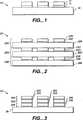
Das monochrome Display
Die TFT-Transistoren
Die Anordnung der
Das Farbdisplay
Die TFT-Transistoren
Zur Herstellung des Farbdisplays
Eine andere Variante eines Farbdisplays ist in der
Die Beschreibung der Erfindung anhand der Ausführungsbeispiele ist selbstverständlich nicht als Beschränkung der Erfindung auf diese zu verstehen. Es versteht sich, daß die in der Beschreibung, in den Zeichnungen sowie in den Ansprüchen offenbarten Merkmale der Erfindung sowohl einzeln als auch in jeder möglichen Kombination für die Verwirklichung der Erfindung wesentlich sein können.The description of the invention with reference to the embodiments is of course not to be construed as limiting the invention thereto. It should be understood that the features of the invention disclosed in the specification, drawings, and claims, both individually and in any possible combination, may be essential to the practice of the invention.
Claims (16)
Translated fromGermanApplications Claiming Priority (4)
| Application Number | Priority Date | Filing Date | Title |
|---|---|---|---|
| US45006803P | 2003-02-24 | 2003-02-24 | |
| US60/450068 | 2003-02-24 | ||
| US10/670,917US7235920B2 (en) | 2003-02-24 | 2003-09-24 | Display device and method of its manufacture |
| US10/670917 | 2003-09-24 |
Publications (2)
| Publication Number | Publication Date |
|---|---|
| DE102004002446A1 DE102004002446A1 (en) | 2004-09-09 |
| DE102004002446B4true DE102004002446B4 (en) | 2012-12-13 |
Family
ID=32853612
Family Applications (1)
| Application Number | Title | Priority Date | Filing Date |
|---|---|---|---|
| DE102004002446AExpired - Fee RelatedDE102004002446B4 (en) | 2003-02-24 | 2004-01-16 | Display device and method for its production |
Country Status (3)
| Country | Link |
|---|---|
| US (1) | US7235920B2 (en) |
| JP (1) | JP2004258656A (en) |
| DE (1) | DE102004002446B4 (en) |
Families Citing this family (5)
| Publication number | Priority date | Publication date | Assignee | Title |
|---|---|---|---|---|
| JP2007080604A (en)* | 2005-09-13 | 2007-03-29 | Seiko Epson Corp | Light emitting device and image forming apparatus using the same |
| US7692610B2 (en)* | 2005-11-30 | 2010-04-06 | Semiconductor Energy Laboratory Co., Ltd. | Display device |
| JP5522991B2 (en)* | 2008-07-11 | 2014-06-18 | キヤノン株式会社 | Organic EL display device |
| DE102012112302A1 (en)* | 2012-12-14 | 2014-06-18 | Osram Opto Semiconductors Gmbh | Display device and method for producing a display device |
| TWI793318B (en)* | 2019-05-03 | 2023-02-21 | 優顯科技股份有限公司 | Micro-semiconductor stack structure, and electronic device thereof |
Citations (4)
| Publication number | Priority date | Publication date | Assignee | Title |
|---|---|---|---|---|
| JPH0667187A (en)* | 1992-08-19 | 1994-03-11 | Seiko Epson Corp | Active matrix liquid crystal display device |
| WO1997006554A2 (en)* | 1995-08-03 | 1997-02-20 | Philips Electronics N.V. | Semiconductor device provided with transparent switching element |
| EP1134811A1 (en)* | 1998-11-17 | 2001-09-19 | Japan Science and Technology Corporation | Transistor and semiconductor device |
| EP1450587A1 (en)* | 2001-12-18 | 2004-08-25 | Seiko Epson Corporation | Light-emitting device, its manufacturing method, electro-optical device, and electronic device |
Family Cites Families (14)
| Publication number | Priority date | Publication date | Assignee | Title |
|---|---|---|---|---|
| FR2681472B1 (en) | 1991-09-18 | 1993-10-29 | Commissariat Energie Atomique | PROCESS FOR PRODUCING THIN FILMS OF SEMICONDUCTOR MATERIAL. |
| US6548956B2 (en)* | 1994-12-13 | 2003-04-15 | The Trustees Of Princeton University | Transparent contacts for organic devices |
| US5989752A (en)* | 1996-05-29 | 1999-11-23 | Chiu; Tzu-Yin | Reconfigurable mask |
| US5886368A (en)* | 1997-07-29 | 1999-03-23 | Micron Technology, Inc. | Transistor with silicon oxycarbide gate and methods of fabrication and use |
| TW439387B (en)* | 1998-12-01 | 2001-06-07 | Sanyo Electric Co | Display device |
| TWI232595B (en)* | 1999-06-04 | 2005-05-11 | Semiconductor Energy Lab | Electroluminescence display device and electronic device |
| JP4472073B2 (en)* | 1999-09-03 | 2010-06-02 | 株式会社半導体エネルギー研究所 | Display device and manufacturing method thereof |
| DE19950839A1 (en) | 1999-10-21 | 2001-05-23 | Fraunhofer Ges Forschung | Device for controlling display elements in a display element array e.g. LCD arrays, comprises separate control circuit to handle each one of multiple display element subarrays |
| JP4727029B2 (en)* | 1999-11-29 | 2011-07-20 | 株式会社半導体エネルギー研究所 | EL display device, electric appliance, and semiconductor element substrate for EL display device |
| TW493282B (en)* | 2000-04-17 | 2002-07-01 | Semiconductor Energy Lab | Self-luminous device and electric machine using the same |
| WO2002016679A1 (en)* | 2000-08-18 | 2002-02-28 | Tohoku Techno Arch Co., Ltd. | Polycrystalline semiconductor material and method of manufacture thereof |
| JP4553470B2 (en)* | 2000-09-13 | 2010-09-29 | 独立行政法人産業技術総合研究所 | Method for growing p-type ZnO-based oxide semiconductor layer and method for manufacturing semiconductor light-emitting device using the same |
| JP4090716B2 (en)* | 2001-09-10 | 2008-05-28 | 雅司 川崎 | Thin film transistor and matrix display device |
| US6975067B2 (en)* | 2002-12-19 | 2005-12-13 | 3M Innovative Properties Company | Organic electroluminescent device and encapsulation method |
- 2003
- 2003-09-24USUS10/670,917patent/US7235920B2/ennot_activeExpired - Lifetime
- 2004
- 2004-01-16DEDE102004002446Apatent/DE102004002446B4/ennot_activeExpired - Fee Related
- 2004-02-24JPJP2004047879Apatent/JP2004258656A/enactivePending
Patent Citations (4)
| Publication number | Priority date | Publication date | Assignee | Title |
|---|---|---|---|---|
| JPH0667187A (en)* | 1992-08-19 | 1994-03-11 | Seiko Epson Corp | Active matrix liquid crystal display device |
| WO1997006554A2 (en)* | 1995-08-03 | 1997-02-20 | Philips Electronics N.V. | Semiconductor device provided with transparent switching element |
| EP1134811A1 (en)* | 1998-11-17 | 2001-09-19 | Japan Science and Technology Corporation | Transistor and semiconductor device |
| EP1450587A1 (en)* | 2001-12-18 | 2004-08-25 | Seiko Epson Corporation | Light-emitting device, its manufacturing method, electro-optical device, and electronic device |
Non-Patent Citations (1)
| Title |
|---|
| Hoffmann, R.L. et al.: "ZnO-based transparent thin-film transistors". In: Appl. Phys. Lett., Vol. 82, No. 5, 3. Feb. 2003, pp. 733-735* |
Also Published As
| Publication number | Publication date |
|---|---|
| JP2004258656A (en) | 2004-09-16 |
| DE102004002446A1 (en) | 2004-09-09 |
| US20050073248A1 (en) | 2005-04-07 |
| US7235920B2 (en) | 2007-06-26 |
Similar Documents
| Publication | Publication Date | Title |
|---|---|---|
| DE102018127655B4 (en) | Organic electroluminescent display device and method for producing the same | |
| DE69838304T2 (en) | Method for producing current-controlled contact hole-emitting light-emitting displays | |
| DE3348002C2 (en) | ||
| DE102016125920B4 (en) | Organic light emitting display device and method of manufacturing the same | |
| DE102016111982B4 (en) | Organic light emitting diode display device | |
| DE10307504B4 (en) | Method for producing an organic electroluminescent component and component produced in this way | |
| DE102006059509B4 (en) | Organic light-emitting element | |
| EP1683210B1 (en) | Full colour organic display with colour filter technology with suitable white emitter material and applications thereof | |
| DE10357472B4 (en) | Organic double panel electroluminescent display and method of making the same | |
| DE102006024448B4 (en) | Organic electroluminescent device and method for its production | |
| DE102013113462A1 (en) | ORGANIC LIGHT DIODE DEVICE AND METHOD FOR MANUFACTURING THE SAME | |
| DE102019134179B4 (en) | DISPLAY DEVICE | |
| DE102015103124B4 (en) | Bi-directional organic display devices and methods for producing double-sided organic display devices | |
| DE102011056448B4 (en) | Organic white light emitting device and display device using the same | |
| DE102016125867B4 (en) | Display device | |
| DE102019128731A1 (en) | Electroluminescent display device | |
| DE112019006327T5 (en) | Display device using semiconductor light emitting device and method of manufacturing the same | |
| DE102017100812B4 (en) | Method for producing an optoelectronic semiconductor component and optoelectronic semiconductor component | |
| DE102014107500B4 (en) | AMOLED DISPLAY PANEL, METHOD FOR PRODUCING A FILM LAYER AND DISPLAY DEVICE | |
| DE102014114778B4 (en) | PIXEL ELEMENT STRUCTURE, ARRAY STRUCTURE AND DISPLAY DEVICE | |
| DE102018129464B4 (en) | LIGHT-EMITTING DISPLAY DEVICE | |
| DE102019132172A1 (en) | ORGANIC LIGHT-EMITTING DISPLAY DEVICE | |
| DE102016125851A1 (en) | Organic light-emitting diode display device | |
| WO2019238394A1 (en) | Arrangement for a display and method | |
| DE112009002522T5 (en) | Display driver units |
Legal Events
| Date | Code | Title | Description |
|---|---|---|---|
| OP8 | Request for examination as to paragraph 44 patent law | ||
| R018 | Grant decision by examination section/examining division | ||
| R020 | Patent grant now final | Effective date:20130314 | |
| R081 | Change of applicant/patentee | Owner name:OSRAM OLED GMBH, DE Free format text:FORMER OWNER: OSRAM OPTO SEMICONDUCTORS GESELLSCHAFT MIT BESCHRAENKTER HAFTUNG, 93055 REGENSBURG, DE Owner name:PICTIVA DISPLAYS INTERNATIONAL LIMITED, IE Free format text:FORMER OWNER: OSRAM OPTO SEMICONDUCTORS GESELLSCHAFT MIT BESCHRAENKTER HAFTUNG, 93055 REGENSBURG, DE | |
| R082 | Change of representative | Representative=s name:EPPING HERMANN FISCHER PATENTANWALTSGESELLSCHA, DE | |
| R081 | Change of applicant/patentee | Owner name:PICTIVA DISPLAYS INTERNATIONAL LIMITED, IE Free format text:FORMER OWNER: OSRAM OLED GMBH, 93049 REGENSBURG, DE | |
| R082 | Change of representative | Representative=s name:EPPING HERMANN FISCHER PATENTANWALTSGESELLSCHA, DE | |
| R079 | Amendment of ipc main class | Free format text:PREVIOUS MAIN CLASS: H01L0051500000 Ipc:H10K0050000000 | |
| R119 | Application deemed withdrawn, or ip right lapsed, due to non-payment of renewal fee |