DE10043600B4 - Device for depositing in particular crystalline layers on one or more, in particular also crystalline substrates - Google Patents
Device for depositing in particular crystalline layers on one or more, in particular also crystalline substratesDownload PDFInfo
- Publication number
- DE10043600B4 DE10043600B4DE10043600ADE10043600ADE10043600B4DE 10043600 B4DE10043600 B4DE 10043600B4DE 10043600 ADE10043600 ADE 10043600ADE 10043600 ADE10043600 ADE 10043600ADE 10043600 B4DE10043600 B4DE 10043600B4
- Authority
- DE
- Germany
- Prior art keywords
- plate
- substrate holder
- process chamber
- crystalline
- cover plate
- Prior art date
- Legal status (The legal status is an assumption and is not a legal conclusion. Google has not performed a legal analysis and makes no representation as to the accuracy of the status listed.)
- Expired - Fee Related
Links
- 239000000758substrateSubstances0.000titleclaimsabstractdescription36
- 238000000151depositionMethods0.000titleclaimsdescription4
- 239000007789gasSubstances0.000claimsabstractdescription28
- 238000000034methodMethods0.000claimsabstractdescription20
- 238000006243chemical reactionMethods0.000claimsabstractdescription5
- 239000000463materialSubstances0.000claimsabstractdescription3
- OKTJSMMVPCPJKN-UHFFFAOYSA-NCarbonChemical compound[C]OKTJSMMVPCPJKN-UHFFFAOYSA-N0.000claimsdescription10
- 229910002804graphiteInorganic materials0.000claimsdescription10
- 239000010439graphiteSubstances0.000claimsdescription10
- VNWKTOKETHGBQD-UHFFFAOYSA-NmethaneChemical compoundCVNWKTOKETHGBQD-UHFFFAOYSA-N0.000description5
- ATUOYWHBWRKTHZ-UHFFFAOYSA-NPropaneChemical compoundCCCATUOYWHBWRKTHZ-UHFFFAOYSA-N0.000description4
- BLRPTPMANUNPDV-UHFFFAOYSA-NSilaneChemical compound[SiH4]BLRPTPMANUNPDV-UHFFFAOYSA-N0.000description3
- 239000000498cooling waterSubstances0.000description3
- 229910000077silaneInorganic materials0.000description3
- 230000000694effectsEffects0.000description2
- 210000000056organAnatomy0.000description2
- 239000001294propaneSubstances0.000description2
- 239000007787solidSubstances0.000description2
- UFHFLCQGNIYNRP-UHFFFAOYSA-NHydrogenChemical compound[H][H]UFHFLCQGNIYNRP-UHFFFAOYSA-N0.000description1
- 230000015572biosynthetic processEffects0.000description1
- 239000011248coating agentSubstances0.000description1
- 238000000576coating methodMethods0.000description1
- 230000000295complement effectEffects0.000description1
- 238000000354decomposition reactionMethods0.000description1
- 230000008021depositionEffects0.000description1
- 238000000407epitaxyMethods0.000description1
- 238000010438heat treatmentMethods0.000description1
- 239000001257hydrogenSubstances0.000description1
- 229910052739hydrogenInorganic materials0.000description1
- 238000009413insulationMethods0.000description1
- 229910021421monocrystalline siliconInorganic materials0.000description1
- 230000000284resting effectEffects0.000description1
Images


Classifications
- C—CHEMISTRY; METALLURGY
- C30—CRYSTAL GROWTH
- C30B—SINGLE-CRYSTAL GROWTH; UNIDIRECTIONAL SOLIDIFICATION OF EUTECTIC MATERIAL OR UNIDIRECTIONAL DEMIXING OF EUTECTOID MATERIAL; REFINING BY ZONE-MELTING OF MATERIAL; PRODUCTION OF A HOMOGENEOUS POLYCRYSTALLINE MATERIAL WITH DEFINED STRUCTURE; SINGLE CRYSTALS OR HOMOGENEOUS POLYCRYSTALLINE MATERIAL WITH DEFINED STRUCTURE; AFTER-TREATMENT OF SINGLE CRYSTALS OR A HOMOGENEOUS POLYCRYSTALLINE MATERIAL WITH DEFINED STRUCTURE; APPARATUS THEREFOR
- C30B25/00—Single-crystal growth by chemical reaction of reactive gases, e.g. chemical vapour-deposition growth
- C30B25/02—Epitaxial-layer growth
- C30B25/12—Substrate holders or susceptors
- C—CHEMISTRY; METALLURGY
- C23—COATING METALLIC MATERIAL; COATING MATERIAL WITH METALLIC MATERIAL; CHEMICAL SURFACE TREATMENT; DIFFUSION TREATMENT OF METALLIC MATERIAL; COATING BY VACUUM EVAPORATION, BY SPUTTERING, BY ION IMPLANTATION OR BY CHEMICAL VAPOUR DEPOSITION, IN GENERAL; INHIBITING CORROSION OF METALLIC MATERIAL OR INCRUSTATION IN GENERAL
- C23C—COATING METALLIC MATERIAL; COATING MATERIAL WITH METALLIC MATERIAL; SURFACE TREATMENT OF METALLIC MATERIAL BY DIFFUSION INTO THE SURFACE, BY CHEMICAL CONVERSION OR SUBSTITUTION; COATING BY VACUUM EVAPORATION, BY SPUTTERING, BY ION IMPLANTATION OR BY CHEMICAL VAPOUR DEPOSITION, IN GENERAL
- C23C16/00—Chemical coating by decomposition of gaseous compounds, without leaving reaction products of surface material in the coating, i.e. chemical vapour deposition [CVD] processes
- C23C16/44—Chemical coating by decomposition of gaseous compounds, without leaving reaction products of surface material in the coating, i.e. chemical vapour deposition [CVD] processes characterised by the method of coating
- C23C16/458—Chemical coating by decomposition of gaseous compounds, without leaving reaction products of surface material in the coating, i.e. chemical vapour deposition [CVD] processes characterised by the method of coating characterised by the method used for supporting substrates in the reaction chamber
- C23C16/4582—Rigid and flat substrates, e.g. plates or discs
- C23C16/4583—Rigid and flat substrates, e.g. plates or discs the substrate being supported substantially horizontally
- C23C16/4584—Rigid and flat substrates, e.g. plates or discs the substrate being supported substantially horizontally the substrate being rotated
Landscapes
- Chemical & Material Sciences (AREA)
- General Chemical & Material Sciences (AREA)
- Chemical Kinetics & Catalysis (AREA)
- Engineering & Computer Science (AREA)
- Materials Engineering (AREA)
- Metallurgy (AREA)
- Organic Chemistry (AREA)
- Mechanical Engineering (AREA)
- Crystallography & Structural Chemistry (AREA)
- Chemical Vapour Deposition (AREA)
- Crystals, And After-Treatments Of Crystals (AREA)
Abstract
Translated fromGermanDescription
Translated fromGermanDie Erfindung betrifft eine Vorrichtung gemäß Gattungsbegriff des Anspruchs 1.The invention relates to a device according to the preamble of
Vorrichtungen zum Abscheiden insbesondere kristalliner Schichten auf einem oder mehreren, insbesondere ebenfalls kristallinen Substraten sind bekannt aus den Patentschriften
Die
Die
Die Erfindung betrifft eine gebrauchsvorteilhafte Weiterbildung des aus der
Vom Anspruch 1 wird hierzu vorgeschlagen, dass die Deckplatte auf ihrer auf dem Substrathalter weisenden Seite mit inert beschichteten oder aus inertem Material bestehenden Platten verkleidet ist.From
Bei der Epitaxie von SiC mit den Reaktionsgasen Silan und Methan/Propan sind die aus Grafit bestehende Trägerplatte und eine ebenfalls aus Grafit bestehende Deckplatte intert beschichtet. Die Beschichtung kann aus TaC oder SiC bestehen. Derartig beschichtete Deck- oder Trägerplatten unterliegen einem Verschleiß, da die Reaktionsgase eine ätzende Wirkung entfalten. Erfindungsgemäß wird die Deckplatte mit austauschbaren Verkleidungsringen verkleidet, welche aus TaC bestehen können. Die Verkleidungsringe halten sich durch gegenseitigen Untergriff. Der innenliegende Ring kann mit seinem Rand auf der Tragschulter eines Trägers liegen, der an einem Gaseinlassorgan sitzt. In einer Variante der Erfindung ist vorgesehen, dass die Verkleidungsringe aus Grafit bestehen und mit TaC oder SiC beschichtet sind.During the epitaxy of SiC with the reaction gases silane and methane / propane, the graphite carrier plate and a cover plate also made of graphite are intert coated. The coating may consist of TaC or SiC. Such coated cover or support plates are subject to wear, since the reaction gases develop a corrosive effect. According to the invention the cover plate is covered with exchangeable lining rings, which may consist of TaC. The fairing rings hold each other by mutual undercut. The inner ring may lie with its edge on the support shoulder of a wearer sitting on a gas inlet member. In a variant of the invention it is provided that the lining rings are made of graphite and coated with TaC or SiC.
Eine derartige Vorrichtung weist vorzugsweise eine auf der Trägerplatte liegende, an den Substrathalter angrenzende Kompensationsplatte auf. Der Rand der Kompensationsplatte folgt dabei der Kontur des Substrathalters. Der Substrathalter ist von ein oder mehreren Kompensationsplatten umschlossen. Es ist bevorzugt eine Vielzahl von Substrathaltern vorgesehen, die planetenartig auf der insbesondere auch drehangetriebenen Trägerplatte angeordnet sind. Die Kompensationsplatten liegen dann segmentartig auf der ringförmigen Trägerplatte. Die Kompensationsplatten können aus TaC oder aus mit TaC- oder SiC-beschichtetem Grafit bestehen. Sie können als Verbrauchsteile ausgetauscht werden. Zur randseitigen Lagerung der kreisscheibenförmigen Substrathalter sind Zentrierringe vorgesehen. Diese Zentrierringe liegen ebenfalls in den Aussparungen der Trägerplatte. An diese Zentrierringe stoßen die runden Randkanten der Kompensationsplatten. Auf den Zentrierringen liegen Abdeckringe, die auch einen gestuften Randabschnitt des Substrathalters überdecken. Die Trägerplatte wird von unten mittels einer zentralen Stützplatte getragen. Dies erfolgt durch Randuntergriff. Oberhalb der Stützplatte kann eine Zugplatte liegen, die sich ebenfalls auf dem Rand der Trägerplatte abstützt. In der Mitte der Zugplatte kann eine Zugstange angreifen, so dass der Rand der Trägerplatte gleichsam eingespannt ist. Die äußere Begrenzung der Prozesskammer wird von einem Gasauslassring ausgebildet, der eine Vielzahl von radialen Gasaustrittsöffnungen besitzt. Dieser soll ebenso wie eine zur Trägerplatte sich parallel und beabstandet erstreckende, ebenfalls rückwärtig beheizte Deckenplatte aus massivem Grafit bestehen. Zufolge dieser Ausgestaltung hat der Gasauslassring eine erhöhte Wärmekapazität und gleichzeitig eine gute Wärmeleitung, so dass von Deckplatte zu Trägerplatte ein stetiger Temperaturverlauf vorliegt.Such a device preferably has a compensation plate lying on the carrier plate and adjacent to the substrate holder. The edge of the compensation plate follows the contour of the substrate holder. The substrate holder is enclosed by one or more compensation plates. It is preferably provided a plurality of substrate holders, which are arranged like a planet on the particular rotation-driven support plate. The compensation plates are then segmented on the annular support plate. The compensation plates can be made of TaC or of TaC- or SiC-coated graphite. They can be exchanged as consumables. For marginal storage of the circular disk-shaped substrate holder centering rings are provided. These centering rings are also in the recesses of the support plate. These centering rings encounter the round marginal edges of the compensation plates. On the centering are cover rings, which also cover a stepped edge portion of the substrate holder. The support plate is supported from below by means of a central support plate. This is done by Randuntergriff. Above the support plate may be a tension plate, which is also supported on the edge of the support plate. In the middle of the tension plate, a pull rod can attack, so that the edge of the support plate is clamped as it were. The outer boundary of the process chamber is formed by a gas outlet ring having a plurality of radial gas outlet openings. This is as well as a parallel to the support plate and spaced extending, also back heated ceiling plate made of solid graphite. According to this embodiment, the gas outlet ring has an increased heat capacity and at the same time a good heat conduction, so that there is a continuous temperature profile from the cover plate to the carrier plate.
Ein Ausführungsbeispiel der Erfindung wird nachfolgend anhand beigefügter Zeichnungen erläutert. Es zeigen:An embodiment of the invention will be explained below with reference to accompanying drawings. Show it:
Die im Ausführungsbeispiel dargestellte Vorrichtung dient zum monokristallinen Abscheiden von SiC-Schichten auf monokristallinen Si-Substraten, diese Substrate können einen Durchmesser von 101,6 mm (= 4 Zoll) besitzen.The apparatus shown in the embodiment is used for monocrystalline deposition of SiC layers on monocrystalline Si substrates, these substrates may have a diameter of 101.6 mm (= 4 inches).
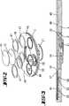
In einem Reaktorgehäuse
Die Trägerplatte
Die Deckplatte
Das Gaseinlassorgan
Die Zuführung des Silans erfolgt durch die Zuleitung
Die Basisfläche
Um die beim Betrieb der Vorrichtung etwa bis auf 1.600°C aufgeheizte Deckplatte
Die Trägerplatte
Wird die Trägerplatte
Am Ausführungsbeispiel sind insgesamt fünf Substrathalter
Claims (4)
Translated fromGermanPriority Applications (9)
| Application Number | Priority Date | Filing Date | Title |
|---|---|---|---|
| DE10043600ADE10043600B4 (en) | 2000-09-01 | 2000-09-01 | Device for depositing in particular crystalline layers on one or more, in particular also crystalline substrates |
| AU2001291797AAU2001291797A1 (en) | 2000-09-01 | 2001-08-24 | Cvd coating device |
| JP2002522573AJP4637450B2 (en) | 2000-09-01 | 2001-08-24 | CVD coating equipment |
| PCT/EP2001/009795WO2002018672A1 (en) | 2000-09-01 | 2001-08-24 | Cvd coating device |
| EP01971962AEP1313891B1 (en) | 2000-09-01 | 2001-08-24 | Cvd coating device |
| DE50114744TDE50114744D1 (en) | 2000-09-01 | 2001-08-24 | CVD COATING DEVICE |
| TW90121443ATW574411B (en) | 2000-09-01 | 2001-08-30 | Device for depositing a coating, particularly a crystal coating, on one or more crystal substrate |
| US10/378,494US7067012B2 (en) | 2000-09-01 | 2003-03-03 | CVD coating device |
| US11/430,725US20060201427A1 (en) | 2000-09-01 | 2006-05-09 | CVD coating device |
Applications Claiming Priority (1)
| Application Number | Priority Date | Filing Date | Title |
|---|---|---|---|
| DE10043600ADE10043600B4 (en) | 2000-09-01 | 2000-09-01 | Device for depositing in particular crystalline layers on one or more, in particular also crystalline substrates |
Publications (2)
| Publication Number | Publication Date |
|---|---|
| DE10043600A1 DE10043600A1 (en) | 2002-03-14 |
| DE10043600B4true DE10043600B4 (en) | 2013-12-05 |
Family
ID=7654974
Family Applications (2)
| Application Number | Title | Priority Date | Filing Date |
|---|---|---|---|
| DE10043600AExpired - Fee RelatedDE10043600B4 (en) | 2000-09-01 | 2000-09-01 | Device for depositing in particular crystalline layers on one or more, in particular also crystalline substrates |
| DE50114744TExpired - LifetimeDE50114744D1 (en) | 2000-09-01 | 2001-08-24 | CVD COATING DEVICE |
Family Applications After (1)
| Application Number | Title | Priority Date | Filing Date |
|---|---|---|---|
| DE50114744TExpired - LifetimeDE50114744D1 (en) | 2000-09-01 | 2001-08-24 | CVD COATING DEVICE |
Country Status (7)
| Country | Link |
|---|---|
| US (2) | US7067012B2 (en) |
| EP (1) | EP1313891B1 (en) |
| JP (1) | JP4637450B2 (en) |
| AU (1) | AU2001291797A1 (en) |
| DE (2) | DE10043600B4 (en) |
| TW (1) | TW574411B (en) |
| WO (1) | WO2002018672A1 (en) |
Cited By (1)
| Publication number | Priority date | Publication date | Assignee | Title |
|---|---|---|---|---|
| WO2021104932A1 (en) | 2019-11-25 | 2021-06-03 | Aixtron Se | Wall-cooled gas-inlet element for a cvd reactor |
Families Citing this family (44)
| Publication number | Priority date | Publication date | Assignee | Title |
|---|---|---|---|---|
| US7574875B2 (en)* | 1999-09-29 | 2009-08-18 | Fibre Ottiche Sud - F.O.S. S.P.A. | Method for vapour deposition on an elongated substrate |
| DE10043599A1 (en)* | 2000-09-01 | 2002-03-14 | Aixtron Ag | Device for depositing, in particular, crystalline layers on one or more, in particular likewise, crystalline substrates |
| DE10043601A1 (en)* | 2000-09-01 | 2002-03-14 | Aixtron Ag | Device and method for depositing, in particular, crystalline layers on, in particular, crystalline substrates |
| US7122844B2 (en) | 2002-05-13 | 2006-10-17 | Cree, Inc. | Susceptor for MOCVD reactor |
| US8366830B2 (en) | 2003-03-04 | 2013-02-05 | Cree, Inc. | Susceptor apparatus for inverted type MOCVD reactor |
| DE10323085A1 (en)* | 2003-05-22 | 2004-12-09 | Aixtron Ag | CVD coater |
| US20050011459A1 (en)* | 2003-07-15 | 2005-01-20 | Heng Liu | Chemical vapor deposition reactor |
| US20050178336A1 (en) | 2003-07-15 | 2005-08-18 | Heng Liu | Chemical vapor deposition reactor having multiple inlets |
| JP2006028625A (en)* | 2004-07-21 | 2006-02-02 | Denso Corp | Cvd apparatus |
| EP1790757B1 (en)* | 2004-07-22 | 2013-08-14 | Toyo Tanso Co., Ltd. | Susceptor |
| JP2006173560A (en)* | 2004-11-16 | 2006-06-29 | Sumitomo Electric Ind Ltd | Wafer guide, metal organic chemical vapor deposition apparatus, and method for depositing nitride-based semiconductor |
| DE102004058521A1 (en)* | 2004-12-04 | 2006-06-14 | Aixtron Ag | Method and apparatus for depositing thick gallium nitrite layers on a sapphire substrate and associated substrate holder |
| DE102005055252A1 (en)* | 2005-11-19 | 2007-05-24 | Aixtron Ag | CVD reactor with slide-mounted susceptor holder |
| US8216419B2 (en) | 2008-03-28 | 2012-07-10 | Bridgelux, Inc. | Drilled CVD shower head |
| US20090096349A1 (en) | 2007-04-26 | 2009-04-16 | Moshtagh Vahid S | Cross flow cvd reactor |
| DE102007023970A1 (en) | 2007-05-23 | 2008-12-04 | Aixtron Ag | Apparatus for coating a plurality of densely packed substrates on a susceptor |
| DE102007026348A1 (en)* | 2007-06-06 | 2008-12-11 | Aixtron Ag | Method and device for temperature control of the surface temperatures of substrates in a CVD reactor |
| US8668775B2 (en) | 2007-10-31 | 2014-03-11 | Toshiba Techno Center Inc. | Machine CVD shower head |
| JP5292963B2 (en)* | 2008-07-16 | 2013-09-18 | 株式会社デンソー | Film forming apparatus and manufacturing method using the same |
| DE102009043848A1 (en) | 2009-08-25 | 2011-03-03 | Aixtron Ag | CVD method and CVD reactor |
| US20110049779A1 (en)* | 2009-08-28 | 2011-03-03 | Applied Materials, Inc. | Substrate carrier design for improved photoluminescence uniformity |
| JP5409413B2 (en)* | 2010-01-26 | 2014-02-05 | 日本パイオニクス株式会社 | III-nitride semiconductor vapor phase growth system |
| US10808319B1 (en)* | 2010-02-26 | 2020-10-20 | Quantum Innovations, Inc. | System and method for vapor deposition of substrates with circular substrate frame that rotates in a planetary motion and curved lens support arms |
| SG183511A1 (en)* | 2010-03-03 | 2012-09-27 | Veeco Instr Inc | Wafer carrier with sloped edge |
| KR20110136583A (en)* | 2010-06-15 | 2011-12-21 | 삼성엘이디 주식회사 | Susceptor and chemical vapor deposition apparatus having the same |
| JP5101665B2 (en)* | 2010-06-30 | 2012-12-19 | 東京エレクトロン株式会社 | Substrate mounting table, substrate processing apparatus, and substrate processing system |
| KR20120083712A (en)* | 2011-01-18 | 2012-07-26 | 삼성엘이디 주식회사 | Susceptor and chemical vapor deposition apparatus comprising the same |
| JP5613083B2 (en)* | 2011-02-28 | 2014-10-22 | 大陽日酸株式会社 | Susceptor cover and vapor phase growth apparatus provided with the susceptor cover |
| JP5867913B2 (en)* | 2011-05-30 | 2016-02-24 | 昭和電工株式会社 | Silicon carbide film CVD system |
| US20130171350A1 (en)* | 2011-12-29 | 2013-07-04 | Intermolecular Inc. | High Throughput Processing Using Metal Organic Chemical Vapor Deposition |
| WO2014132948A1 (en) | 2013-02-27 | 2014-09-04 | 東洋炭素株式会社 | Susceptor |
| US9273413B2 (en) | 2013-03-14 | 2016-03-01 | Veeco Instruments Inc. | Wafer carrier with temperature distribution control |
| CN104342758B (en)* | 2013-07-24 | 2017-07-21 | 北京北方微电子基地设备工艺研究中心有限责任公司 | pressure ring and plasma processing device |
| JP6097681B2 (en) | 2013-12-24 | 2017-03-15 | 昭和電工株式会社 | SiC epitaxial wafer manufacturing apparatus and SiC epitaxial wafer manufacturing method |
| US9396983B2 (en)* | 2014-06-02 | 2016-07-19 | Epistar Corporation | Susceptor |
| JP6335683B2 (en)* | 2014-06-30 | 2018-05-30 | 昭和電工株式会社 | SiC epitaxial wafer manufacturing equipment |
| US20160033070A1 (en)* | 2014-08-01 | 2016-02-04 | Applied Materials, Inc. | Recursive pumping member |
| DE102016115614A1 (en) | 2016-08-23 | 2018-03-01 | Aixtron Se | Susceptor for a CVD reactor |
| KR102369676B1 (en) | 2017-04-10 | 2022-03-04 | 삼성디스플레이 주식회사 | Apparatus and method for manufacturing a display apparatus |
| JP6621971B2 (en) | 2017-10-18 | 2019-12-18 | 新日本テクノカーボン株式会社 | Susceptor |
| TW202425214A (en)* | 2017-10-27 | 2024-06-16 | 美商應用材料股份有限公司 | Single wafer processing environments with spatial separation |
| JP7055004B2 (en)* | 2017-11-13 | 2022-04-15 | 昭和電工株式会社 | Manufacturing method of SiC epitaxial wafer |
| KR102535194B1 (en)* | 2018-04-03 | 2023-05-22 | 주성엔지니어링(주) | Apparatus for Processing Substrate |
| DE102019105913A1 (en) | 2019-03-08 | 2020-09-10 | Aixtron Se | Susceptor arrangement of a CVD reactor |
Citations (6)
| Publication number | Priority date | Publication date | Assignee | Title |
|---|---|---|---|---|
| US5027746A (en)* | 1988-03-22 | 1991-07-02 | U.S. Philips Corporation | Epitaxial reactor having a wall which is protected from deposits |
| WO1996023913A1 (en)* | 1995-01-31 | 1996-08-08 | Abb Research Limited | Method and device for protecting the susceptor during epitaxial growth by cvd |
| EP0838841A2 (en)* | 1996-10-18 | 1998-04-29 | Applied Materials, Inc. | Inductively coupled parallel-plate plasma reactor with a conical dome |
| US5788777A (en)* | 1997-03-06 | 1998-08-04 | Burk, Jr.; Albert A. | Susceptor for an epitaxial growth factor |
| US5863339A (en)* | 1995-12-15 | 1999-01-26 | Nec Corporation | Chamber etching of plasma processing apparatus |
| DE19813523C2 (en)* | 1998-03-26 | 2000-03-02 | Aixtron Ag | CVD reactor and its use |
Family Cites Families (9)
| Publication number | Priority date | Publication date | Assignee | Title |
|---|---|---|---|---|
| US502746A (en)* | 1893-08-08 | Den neave | ||
| JPS5540756Y2 (en)* | 1976-03-15 | 1980-09-24 | ||
| JPS6058613A (en)* | 1983-09-12 | 1985-04-04 | Hitachi Ltd | Epitaxial apparatus |
| JPH02212394A (en)* | 1989-02-13 | 1990-08-23 | Mitsui Eng & Shipbuild Co Ltd | Susceptor |
| US5820686A (en)* | 1993-01-21 | 1998-10-13 | Moore Epitaxial, Inc. | Multi-layer susceptor for rapid thermal process reactors |
| JPH06310438A (en)* | 1993-04-22 | 1994-11-04 | Mitsubishi Electric Corp | Substrate holder and apparatus for vapor growth of compound semiconductor |
| JP3317781B2 (en)* | 1994-06-08 | 2002-08-26 | 東芝セラミックス株式会社 | Method of manufacturing susceptor for heat treatment of semiconductor wafer |
| JP3872838B2 (en)* | 1996-04-30 | 2007-01-24 | 松下電器産業株式会社 | Crystal growth method |
| JP3853453B2 (en)* | 1997-01-06 | 2006-12-06 | 徳山東芝セラミックス株式会社 | Vertical susceptor for vapor phase growth |
- 2000
- 2000-09-01DEDE10043600Apatent/DE10043600B4/ennot_activeExpired - Fee Related
- 2001
- 2001-08-24AUAU2001291797Apatent/AU2001291797A1/ennot_activeAbandoned
- 2001-08-24WOPCT/EP2001/009795patent/WO2002018672A1/enactiveApplication Filing
- 2001-08-24EPEP01971962Apatent/EP1313891B1/ennot_activeExpired - Lifetime
- 2001-08-24JPJP2002522573Apatent/JP4637450B2/ennot_activeExpired - Fee Related
- 2001-08-24DEDE50114744Tpatent/DE50114744D1/ennot_activeExpired - Lifetime
- 2001-08-30TWTW90121443Apatent/TW574411B/ennot_activeIP Right Cessation
- 2003
- 2003-03-03USUS10/378,494patent/US7067012B2/ennot_activeExpired - Fee Related
- 2006
- 2006-05-09USUS11/430,725patent/US20060201427A1/ennot_activeAbandoned
Patent Citations (6)
| Publication number | Priority date | Publication date | Assignee | Title |
|---|---|---|---|---|
| US5027746A (en)* | 1988-03-22 | 1991-07-02 | U.S. Philips Corporation | Epitaxial reactor having a wall which is protected from deposits |
| WO1996023913A1 (en)* | 1995-01-31 | 1996-08-08 | Abb Research Limited | Method and device for protecting the susceptor during epitaxial growth by cvd |
| US5863339A (en)* | 1995-12-15 | 1999-01-26 | Nec Corporation | Chamber etching of plasma processing apparatus |
| EP0838841A2 (en)* | 1996-10-18 | 1998-04-29 | Applied Materials, Inc. | Inductively coupled parallel-plate plasma reactor with a conical dome |
| US5788777A (en)* | 1997-03-06 | 1998-08-04 | Burk, Jr.; Albert A. | Susceptor for an epitaxial growth factor |
| DE19813523C2 (en)* | 1998-03-26 | 2000-03-02 | Aixtron Ag | CVD reactor and its use |
Cited By (1)
| Publication number | Priority date | Publication date | Assignee | Title |
|---|---|---|---|---|
| WO2021104932A1 (en) | 2019-11-25 | 2021-06-03 | Aixtron Se | Wall-cooled gas-inlet element for a cvd reactor |
Also Published As
| Publication number | Publication date |
|---|---|
| AU2001291797A1 (en) | 2002-03-13 |
| JP2004507619A (en) | 2004-03-11 |
| JP4637450B2 (en) | 2011-02-23 |
| US20060201427A1 (en) | 2006-09-14 |
| EP1313891B1 (en) | 2009-03-04 |
| DE50114744D1 (en) | 2009-04-16 |
| WO2002018672A1 (en) | 2002-03-07 |
| EP1313891A1 (en) | 2003-05-28 |
| TW574411B (en) | 2004-02-01 |
| US20030221624A1 (en) | 2003-12-04 |
| DE10043600A1 (en) | 2002-03-14 |
| US7067012B2 (en) | 2006-06-27 |
Similar Documents
| Publication | Publication Date | Title |
|---|---|---|
| DE10043600B4 (en) | Device for depositing in particular crystalline layers on one or more, in particular also crystalline substrates | |
| EP1313897B1 (en) | Device and method for the deposition of, in particular, crystalline layers on, in particular, crystalline substrates | |
| EP1397528B1 (en) | Cvd reactor with exhaust ring made of graphite | |
| EP1948845B1 (en) | Cvd reactor with slidingly mounted susceptor holder | |
| DE10241964B4 (en) | Coating gas generators and processes | |
| EP2010693B1 (en) | Cvd reactor having a process chamber lid which can be lowered | |
| DE60006095T2 (en) | REACTOR CHAMBER FOR AN EPITAXIS REACTOR | |
| DE3301288C2 (en) | ||
| EP2155926B1 (en) | Device for the temperature control of the surface temperatures of substrates in a cvd reactor | |
| DE102009044276A1 (en) | CVD reactor with multi-zone gas cushion substrate holder | |
| DE10320597A1 (en) | Method and device for depositing semiconductor layers with two process gases, one of which is preconditioned | |
| DE102005055468A1 (en) | Coating one or more substrates comprises supplying gases to process chamber via chambers with gas outlet openings | |
| DE112014003693B4 (en) | Epitaxial reactor | |
| DE102021103245A1 (en) | CVD reactor with a process chamber floor that rises in a flow zone | |
| DE10323085A1 (en) | CVD coater | |
| WO2003038144A1 (en) | Method and device for depositing especially crystalline layers onto especially crystalline substrates | |
| DE112012000726T5 (en) | A susceptor and method of making an epitaxial wafer using the same | |
| DE1963207B2 (en) | DEVICE FOR EPITACTIC DEPOSITION OF SEMICONDUCTOR MATERIAL ON A SUBSTRAT | |
| DE102005056324A1 (en) | CVD reactor with exchangeable process chamber ceiling | |
| DE102014222865A1 (en) | Fluidized bed reactor for the production of polycrystalline silicon granules and method for assembling such a fluidized bed reactor | |
| DE102016001728B3 (en) | Einkristallzüchtungsvorrichtung | |
| DE102020123546A1 (en) | CVD reactor with a cooling surface with increased emissivity in some areas | |
| DE102005056322A1 (en) | Apparatus for depositing a film on a substrate, especially for semiconductor production, comprises a process chamber that contains a substrate holder and is supplied with process gases through coaxial inlet ports | |
| DE69613855T2 (en) | DEVICE FOR HEAT TREATING OBJECTS | |
| AT225750B (en) | Process for manufacturing semiconductor material |
Legal Events
| Date | Code | Title | Description |
|---|---|---|---|
| 8110 | Request for examination paragraph 44 | ||
| 8127 | New person/name/address of the applicant | Owner name:AIXTRON AG, 52134 HERZOGENRATH, DE | |
| R082 | Change of representative | Representative=s name:RIEDER & PARTNER PATENTANWAELTE - RECHTSANWALT, 42 Representative=s name:RIEDER & PARTNER PATENTANWAELTE - RECHTSANWALT, DE | |
| R016 | Response to examination communication | ||
| R081 | Change of applicant/patentee | Owner name:AIXTRON SE, DE Free format text:FORMER OWNER: AIXTRON AG, 52134 HERZOGENRATH, DE Effective date:20111104 | |
| R082 | Change of representative | Representative=s name:RIEDER & PARTNER PATENTANWAELTE - RECHTSANWALT, DE Effective date:20111104 Representative=s name:RIEDER & PARTNER MBB PATENTANWAELTE - RECHTSAN, DE Effective date:20111104 | |
| R016 | Response to examination communication | ||
| R018 | Grant decision by examination section/examining division | ||
| R020 | Patent grant now final | Effective date:20140306 | |
| R119 | Application deemed withdrawn, or ip right lapsed, due to non-payment of renewal fee | ||
| R119 | Application deemed withdrawn, or ip right lapsed, due to non-payment of renewal fee | Effective date:20150401 |