CN218633892U - A thyristor circuit and electronic equipment - Google Patents
A thyristor circuit and electronic equipmentDownload PDFInfo
- Publication number
- CN218633892U CN218633892UCN202222392498.3UCN202222392498UCN218633892UCN 218633892 UCN218633892 UCN 218633892UCN 202222392498 UCN202222392498 UCN 202222392498UCN 218633892 UCN218633892 UCN 218633892U
- Authority
- CN
- China
- Prior art keywords
- module
- resistor
- zero
- terminal
- thyristor
- Prior art date
- Legal status (The legal status is an assumption and is not a legal conclusion. Google has not performed a legal analysis and makes no representation as to the accuracy of the status listed.)
- Active
Links
Images


Landscapes
- Power Conversion In General (AREA)
Abstract
Translated fromChinese
Description
Translated fromChinese技术领域technical field
本申请实施例涉及电能控制技术领域,尤其涉及一种可控硅电路及电子设备。The embodiments of the present application relate to the technical field of electric energy control, and in particular to a thyristor circuit and electronic equipment.
背景技术Background technique
在交流电路中,由于交流电的电流方向按交流电频率发生交替变化,在前半周期,电流从第一极流向第二极,在后半周期,电流流动方向相反,从第二极流向第一极,因而在交流电路中需要可以双向导通的半导体器件。可控硅为交流电路中的常用可以双向导通的半导体器件,可用作可控整流、无触点开关等功能。双向可控硅只要在控制极(G极)施加驱动信号,便可控制双向可控硅的导通。In an AC circuit, since the direction of the alternating current changes alternately according to the frequency of the alternating current, in the first half cycle, the current flows from the first pole to the second pole, and in the second half cycle, the current flows in the opposite direction, from the second pole to the first pole. Therefore, semiconductor devices that can conduct bidirectionally are required in AC circuits. Thyristor is a semiconductor device commonly used in AC circuits that can conduct bidirectionally, and can be used for functions such as controllable rectification and non-contact switch. As long as a driving signal is applied to the control pole (G pole) of the bidirectional thyristor, the conduction of the bidirectional thyristor can be controlled.
双向可控硅工作时,由于流过双向可控硅的第一主电极和第二主电极之间的电流为双向流动的交流电,当交流电正处于波峰或者波谷时,导通或切断可控硅回路会造成很大的冲击电流和冲击电压,容易损坏器件和造成谐波干扰。When the bidirectional thyristor is working, since the current flowing between the first main electrode and the second main electrode of the bidirectional thyristor is a bidirectional alternating current, when the alternating current is at the peak or valley, the thyristor is turned on or off. The circuit will cause a large impulse current and impulse voltage, which is easy to damage the device and cause harmonic interference.
相关技术的交流电路中,直接根据驱动信号的导通而导通双向可控硅,可能会在交流电正处于波峰或波谷时导通或切断可控硅回路,容易损坏器件和造成谐波干扰,导致可控硅电路安全性低,抗干扰弱。In the AC circuit of the related art, the bidirectional thyristor is turned on directly according to the conduction of the driving signal, which may turn on or cut off the thyristor circuit when the alternating current is at the peak or valley, which is easy to damage the device and cause harmonic interference. As a result, the safety of the thyristor circuit is low and the anti-interference is weak.
实用新型内容Utility model content
本申请实施例提供了一种可控硅电路及电子设备,能够解决可控硅电路安全性低的问题,提升可控硅电路的安全性和抗干扰能力。The embodiments of the present application provide a thyristor circuit and electronic equipment, which can solve the problem of low safety of the thyristor circuit and improve the safety and anti-interference ability of the thyristor circuit.
本申请实施例提供了一种可控硅电路,用于向负载模块供电,其特征在于,包括:火线端子、零线端子、第一控制模块和可控硅模块;An embodiment of the present application provides a thyristor circuit for supplying power to a load module, which is characterized in that it includes: a live wire terminal, a neutral wire terminal, a first control module, and a thyristor module;
所述火线端子和所述零线端子均与所述第一控制模块的输入端以及过零检测端连接,所述过零检测端用于检测交流电的过零信号;Both the live wire terminal and the neutral wire terminal are connected to the input terminal of the first control module and the zero-crossing detection terminal, and the zero-crossing detection terminal is used to detect the zero-crossing signal of the alternating current;
所述第一控制模块的输出端与所述可控硅模块的控制端连接,所述第一控制模块用于检测到过零信号后通过输出端传输电平信号给所述可控硅模块的控制端;The output terminal of the first control module is connected to the control terminal of the thyristor module, and the first control module is used to transmit a level signal to the thyristor module through the output terminal after detecting the zero-crossing signal Control terminal;
所述可控硅模块的第一端与所述零线端子连接,第二端用于与所述负载模块连接,所述可控硅模块用于根据控制端接收到的电平信号使得第一端和第二端导通。The first end of the silicon controlled rectifier module is connected to the neutral line terminal, the second end is used to connect to the load module, and the silicon controlled rectifier module is used to make the first terminal and the second terminal conduction.
本申请实施例还提供了一种电子设备,包括上述所述的可控硅电路。The embodiment of the present application also provides an electronic device, including the above-mentioned thyristor circuit.
通过第一控制模块在检测到过零信号后通过输出端传输电平信号给可控硅模块的控制端,以使可控硅模块第一端和第二端导通,从而给负载模块供电,避免了出现在交流电处于波峰或波谷时导通或切断可控硅回路的情况,提升可控硅电路的安全性和抗干扰能力。After the first control module detects the zero-crossing signal, it transmits a level signal to the control terminal of the thyristor module through the output terminal, so that the first terminal and the second terminal of the thyristor module are turned on, thereby supplying power to the load module, It avoids the situation of turning on or cutting off the thyristor circuit when the alternating current is at a peak or valley, and improves the safety and anti-interference ability of the thyristor circuit.
附图说明Description of drawings
图1是可控硅模块给负载供电的工作原理示意图;Figure 1 is a schematic diagram of the working principle of the thyristor module supplying power to the load;
图2是本申请实施例提供的一种可控硅电路的第一电路示意图;Fig. 2 is a first schematic circuit diagram of a silicon controlled rectifier circuit provided in an embodiment of the present application;
图3是本申请实施例提供的过零开通示意图;Fig. 3 is a schematic diagram of zero-crossing activation provided by the embodiment of the present application;
图4是本申请实施例提供的第一控制模块的电路示意图;Fig. 4 is a schematic circuit diagram of a first control module provided by an embodiment of the present application;
图5是本申请实施例提供的驱动模块的电路示意图;Fig. 5 is a schematic circuit diagram of a driving module provided by an embodiment of the present application;
图6是本申请实施例提供的过零检测模块的电路示意图;6 is a schematic circuit diagram of a zero-crossing detection module provided in an embodiment of the present application;
图7是本申请实施例提供的第二控制模块检测波形示意图;Fig. 7 is a schematic diagram of the detection waveform of the second control module provided by the embodiment of the present application;
图8是本申请实施例提供的可控硅模块的电路示意图;FIG. 8 is a schematic circuit diagram of a silicon controlled rectifier module provided in an embodiment of the present application;
图9是可控硅模块的工作象限示意图;Fig. 9 is a schematic diagram of the working quadrant of the thyristor module;
图10是本申请实施例提供的一种可控硅电路的第二电路原理图。FIG. 10 is a second circuit schematic diagram of a silicon controlled rectifier circuit provided in an embodiment of the present application.
具体实施方式Detailed ways
下面将结合本实用新型实施例中的附图,对本实用新型实施例中的技术方案进行清楚、完整地描述,显然,所描述的实施例仅仅是本实用新型一部分实施例,而不是全部的实施例。The technical solutions in the embodiments of the present invention will be clearly and completely described below in conjunction with the accompanying drawings in the embodiments of the present invention. Obviously, the described embodiments are only part of the embodiments of the present invention, not all of them. example.
可控硅模块是交流电路中常用的一种功率器件,可用作于可控整流、无触点开关等功能。在交流回路中,由于交流电的电流方向按交流电频率发生交替变化,在前半周周期里,电流从一极流向另一极,在后半周周期里,电流流动方向相反,因此需要可以双向导通的半导体器件,而双向可控硅模块就是具备双向导通的半导体器件,只要在可控硅模块的控制极(控制端)施加驱动信号,便可控制双向可控硅导通。Thyristor module is a power device commonly used in AC circuits, which can be used for functions such as controllable rectification and non-contact switch. In an AC circuit, since the direction of the alternating current changes alternately according to the frequency of the alternating current, in the first half of the cycle, the current flows from one pole to the other, and in the second half of the cycle, the current flows in the opposite direction, so bidirectional conduction is required. Semiconductor devices, and the bidirectional thyristor module is a semiconductor device with bidirectional conduction. As long as a driving signal is applied to the control electrode (control terminal) of the thyristor module, the bidirectional thyristor can be controlled to conduct.
图1是可控硅模块给负载供电的工作原理示意图,如图1所示,由于流过双向可控硅的第一主电极T1端和第二主电极T2端之间的电流为双向流动的交流电,当交流电处于波峰或者波谷时,导通可控硅回路或者切断可控硅回路会造成很大的冲击电流和冲击电压,容易损坏器件和造成谐波干扰。因此,为了避免损坏器件,需要让交流电过零时导通可控硅回路或者切断可控硅回路,才能把冲击电压和冲击电流降到最小,从而保护器件和减少谐波干扰。为此,提出一种可控硅电路,以实现过零导通可控硅回路。Figure 1 is a schematic diagram of the working principle of the thyristor module supplying power to the load. As shown in Figure 1, since the current flowing between the first main electrode T1 and the second main electrode T2 of the bidirectional thyristor flows bidirectionally AC power, when the AC power is at its peak or trough, turning on or cutting off the thyristor circuit will cause a large surge current and voltage, which will easily damage the device and cause harmonic interference. Therefore, in order to avoid damage to the device, it is necessary to turn on the thyristor circuit or cut off the thyristor circuit when the alternating current crosses zero, so as to minimize the impact voltage and current, thereby protecting the device and reducing harmonic interference. For this reason, a thyristor circuit is proposed to realize zero-crossing conduction of the thyristor circuit.
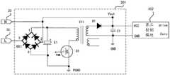
图2给出了本申请实施例提供的一种可控硅电路的第一电路图,该可控硅电路用于向负载50供电,其中负载50为实际产品在工作时使用的负载,包括阻性负载、感性负载或容性负载。如图2所示,该可控硅电路包括火线端子10、零线端子20、第一控制模块30和可控硅模块40。火线端子10用于接入交流电的火线,零线端子20用于接入交流电的零线。第一控制模块30包括四个端口,分别为两个输入端、输出端drive和过零检测端Zero。其中输入端用于接入交流电,为第一控制模块30供电,以实现第一控制模块30的正常运作。火线端子10和零线端子20均与第一控制模块30的输入端以及过零检测端Zero连接,过零检测端Zero用于检测交流电的过零信号。第一控制模块30的输出端drive与可控硅模块40的控制端G1连接,第一控制模块30用于检测到过零信号后通过输出端drive传输电平信号给可控硅模块40的控制端G1。可控硅模块40的第一端与零线端子20连接,第二端用于与负载50模块连接,可控硅模块40用于根据控制端G1接收到的电平信号使得第一端和第二端导通,以向负载50模块供电。通过过零检测端Zero检测到交流电过零后才输出电平信号使得可控硅模块40导通,避免了当交流电处于波峰或者波谷时导通可控硅回路或者切断可控硅回路造成很大的冲击电流和冲击电压,容易损坏器件和造成谐波干扰的情况,提升了可控硅电路的安全性和抗干扰能力。Figure 2 shows the first circuit diagram of a silicon controlled rectifier circuit provided by the embodiment of the present application, the silicon controlled rectifier circuit is used to supply power to a
图3是本申请实施例提供的过零开通示意图,由上述可控硅电路进行负载50供电时,如图3所示,当第一控制模块30的过零检测端Zero检测到交流电的电压在过零点后时,则第一控制模块30的输出端drive输出电平信号给可控硅模块40的控制端G1,可控硅模块40的控制端G1接收到驱动信号PWM使对应的第一端和第二端导通,第二端与负载50连接,使得给负载50供电。由于过零点后,在零点附近交流电的电压电流会很小,因此不会造成很大的电压冲击和电流冲击,从而达到保护器件和降低谐波的目的。Fig. 3 is a schematic diagram of the zero-crossing turn-on provided by the embodiment of the present application. When the
图4是本申请实施例提供的第一控制模块30的电路示意图,如图4所示,第一控制模块30包括驱动模块301、第二控制模块302和过零检测模块303。驱动模块301用于接收驱动信号PWM,根据驱动信号PWM将通过火线端子10 和零线端子20输入的电源传输给第二控制模块302。火线端子10和零线端子 20分别与驱动模块301的第一电源端和第二电源端连接,以实现交流电的输入。驱动模块301的第一输出端与第二控制模块302的输入端VCC连接,在接收到驱动信号PWM时,对应驱动信号PWM的控制将工作电流传输给第二控制模块302。驱动模块301的第二输出端与第二控制模块302的接地端GND连接,驱动模块301的第五端接地。第二控制模块302的过零检测端Zero与过零检测模块303的第一端连接,过零检测模块303的第二端与火线端子10连接,过零检测模块303的第三端与零线端子20连接,过零检测模块303第四端接地,过零检测模块303能将火线端子10和零线端子20的电流电压信号传输给第二控制控制模块的过零检测端Zero,从而使得第二控制模块302可以通过过零检测端 Zero获知对应的可控硅电路中的交流电源的瞬时电压状态。第二控制模块302 的输出端drive与可控硅模块40的控制端G1连接,可控硅模块40的第一端与零线端子20连接,第二端与负载50模块连接。负载50模块的第一端与可控硅模块40第二端连接,第二端与火线端子10连接。请参考图3,基于交流电源的瞬时电压状态,每当交流电在过零点附近时,第二控制模块302的输出端drive 输出电平信号给所述可控硅模块40的控制端G1,可控硅模块40基于控制端 G1接收到的电平信号控制第一端和第二端的导通状态,从而让交流电过零时导通可控硅回路或者切断可控硅回路,能把冲击降到最小,从而保护器件和减小谐波干扰,实现对负载50模块的安全供电。通过过零检测端Zero检测到交流电过零后才输出电平信号使得可控硅模块40导通,避免了当交流电处于波峰或者波谷时导通可控硅回路或者切断可控硅回路造成很大的冲击电流和冲击电压,容易损坏器件和造成谐波干扰的情况,提升可控硅电路的安全性和抗干扰能力。FIG. 4 is a schematic circuit diagram of the
需要说明的是,第二控制模块302为单片机或控制芯片。It should be noted that the
图5是本申请实施例提供的驱动模块301的电路示意图,如图5所示,驱动模块301包括整流桥BD1、第一控制开关Q1、变压器TF1和第一二极管D1,其中整流桥BD1用于将交流电转为直流电,变压器TF1用于传递能量和电压变比。整流桥BD1的一个交流输入端2引脚与零线端子20连接,另一个交流输入端3引脚与火线端子10连接,整流桥BD1的正极输出端1引脚与变压器TF1的初级侧第一引脚连接,整流桥BD1的负极输出端4引脚与第一控制开关Q1的第一端连接并接地,第一控制开关Q1的第二端用于接收驱动信号PWM,第三端与变压器TF1的初级侧的第二引脚连接,第一控制开关Q1用于根据驱动信号PWM 实现第一端和第三端的导通,从而使得整流桥BD1的正极输出端1引脚和负极输出端4引脚流出的电流传输到变压器TF1的初级侧的第一引脚和第二引脚。基于驱动信号PWM控制第一控制开关Q1的导通或关断时间,使得变压器TF1的次级侧得到一个稳定的输出电压Vout。变压器TF1的次级侧的第三引脚与第一二极管D1的阳极相连,第一二极管D1的阴极与零线端子20以及第二控制模块 302的输入端VCC连接,变压器TF1的次级侧的第四引脚与第二控制模块302的接地端GND连接。变压器TF1的次级侧的输出电压Vout正常建立后经过第一二极管D1后流进第二控制模块302的输入端VCC,以实现对第二控制模块302的供电。第一二极管D1为整流二极管,起到防止电压反向流动的作用。Fig. 5 is a schematic circuit diagram of the
其中,第一控制开关Q1包括场效应管,场效应管的源极与整流桥BD1的负极输出端4引脚连接,栅极用于接收驱动信号PWM,漏极与变压器TF1的初级侧的第二引脚连接,场效应管用于根据栅极接收到的驱动信号PWM使得源极和漏极导通。通过驱动信号PWM可以控制变压器TF1初级侧的导通,同时可以控制变压器TF1初级侧的电压值,从而实现控制变压器TF1次级侧的输出的电压值。Wherein, the first control switch Q1 includes a field effect transistor, the source of the field effect transistor is connected to the
需要说明的是,整流桥BD1的负极输出端4引脚接地为PGND。It should be noted that the ground of
需要说明的是,第一控制开关Q1除了是场效应管(MOS管)外,还可以是其他开关管,如IGBT等可控器件。It should be noted that, besides a field effect transistor (MOS transistor), the first control switch Q1 may also be other switch transistors, such as IGBT and other controllable devices.
其中,驱动模块301还包括电解电容E1和第一电容C1。电解电容E1的正极与整流桥BD1的正极输出端1引脚连接,负极与整流桥BD1的负极输出端4 引脚连接。电解电容E1用于稳定整流桥BD1转换后的直流电流的电压,容值一般较大。第一电容C1的第一端与第一二极管D1的阴极连接,第二端与第二控制模块302的接地端GND连接。第一电容C1用于稳定Vout电压。Wherein, the
在交流电经整流桥BD1转换成直流电后,通过驱动模块301实现直流电输入第二控制模块302的导通控制,实现驱动输入和驱动开关的功能,使得在接收到驱动信号PWM后导通电流输入第二控制模块302,以实现第二控制模块302 的供电,保障第二控制模块302的运行,为后续可控硅模块40的控制端G1的驱动信号PWM提供基础电流。After the alternating current is converted into direct current by the rectifier bridge BD1, the conduction control of the direct current input to the
图6是本申请实施例提供的过零检测模块303的电路示意图,如图6所示,过零检测模块303包括电阻模块3031、第一电阻R1、第二电阻R2、第二二极管 D2和第三二极管D3。电阻模块3031的第一端与火线端子10连接,第二端与第二二极管D2的阳极以及第一电阻R1的第一端连接。电阻模块3031起到限流作用,以保护电路器件。第二二极管D2的阴极与零线端子20以及第二电阻R2的第一端连接。第一电阻R1的第二端与第三二极管D3的阳极、第二电阻R2的第二端以及第二控制模块302的过零检测端Zero连接,并接地。第三二极管D3 的阴极与第一电阻R1的第一端以及所述第二控制模块302的过零检测端Zero 连接。第二二极管D2和第三二极管D3提供火线端子10和零线端子20之间的通路。Figure 6 is a schematic circuit diagram of the zero-crossing
当交流电为正半周期时,即火线端子10的电流为正,零线端子20电流为负,设零线端子20处的电压为Vout,因此检测回路为:火线端子10-电阻模块 3031-第二二极管D2-零线端子20。当第二二极管D2导通时,设第三二极管D3 的阴极与第一电阻R1第一端处为VAD,则VAD处的电压为:VAD=Vout+VD2,其中VD2为第二二极管D2的导通压降,一般为0.7V。VAD处将高电平信号传输至第二控制模块302的过零检测端Zero引脚,则第二控制模块302检测到高电平。When the alternating current is a positive half cycle, that is, the current of the
当交流电处于负半周期时,则火线端子10的电流为负,零线端子20的电流为正,则检测回路为:零线端子20-第二电阻R2-第三二极管D3-电阻模块 3031-火线端子10。当第三二极管D3导通时,基于第一电阻R1的第二端和第三二极管D3的阳极都接地GND,则VAD处的电压相对于地GND电压为: VAD=GND-VD3=GND-0.7V,即VAD处的电压相对于地而言是-0.7V,则对应的第二控制模块302的过零检测端Zero的引脚的信号为低电平。When the alternating current is in the negative half cycle, the current of
由此,在第二控制模块302中可以得到过零检测模块303对应的电路仿真得到波形如7所示,上图为交流电波形,下图为第二控制模块302的过零检测端Zero引脚检测到波形。从波形图可以看出,每当交流电在过零点附近时,过零检测端Zero引脚检测到的信号便会出现一次高低电平的转换,因此,只需要第二控制模块302检测到过零检测端Zero引脚的接收到的信号进行电平转换,即可判断交流电产生了过零信号,第二控制模块302根据该过零信号通过输出端drive输出电平信号控制可控硅模块40的导通状态。通过过零检测模块303实现过零信号的检测,使得在交流电信号过零后才发送对应的电平信号至可控硅模块40的控制端G1进行导通控制,从而避免了当交流电处于波峰或者波谷时导通可控硅回路或者切断可控硅回路造成很大的冲击电流和冲击电压,容易损坏器件和造成谐波干扰的情况,提升了可控硅电路的安全性和抗干扰能力。Thus, in the
其中,电阻模块3031包括第八电阻R8和第九电阻R9;第八电阻R8的第一端与火线端子10连接,第二端与第九电阻R9的第一端连接;第九电阻R9的第二端与第二二极管D2的阳极以及第一电阻R1的第一端连接。通过第八电阻R8 和第九电阻R9串联设置,实现限流作用,以保护电路。Wherein, the
在一实施例中,电阻模块3031中的第八电阻R8和第九电阻R9可以并联连接。第八电阻R8的第一端和第九电阻R9的第一端均与火线端子10连接,第八电阻R8的第二端和第九电阻R9的第二端均与第二二极管D2的阳极以及第一电阻R1的第一端连接。In an embodiment, the eighth resistor R8 and the ninth resistor R9 in the
在一实施例中,电阻模块3031中对应的电阻数据量以及电阻的串并联方式可以根据实际情况进行设置,只要能实现限流作用即可。In an embodiment, the corresponding resistance data amount and the series-parallel connection mode of the resistance in the
在一实施例中,过零检测模块303还包括第四二极管D4;第四二极管D4的阳极与第一电阻R1的第一端连接,阴极与第二控制模块302的过零检测端Zero。当第二二极管D2导通时,VAD处的电压为:VAD=Vout+0.7V,其中0.7V为第二二极管D2的压降。一般第二控制模块302为MCU,最大耐压值为Vout+0.5V左右,因此VAD处的电压超过MCU的最大耐压,直接将VAD处得电压输送给第二控制模块302,则容易导致损坏MCU。为了避免进入第二控制模块302中的电压过高,增加第四二极管D4,可以抵消第二二极管D2的管压降,则最终进入第二控制模块302的过零检测端Zero引脚的电压为Vzero=Vout+0.7V-0.7V=Vout,从而保证了第二控制模块302的过零检测端Zero引脚接收到的电压Vzero不会超过MCU的最大耐压,从而起到保护第二控制模块302的作用。In one embodiment, the zero-crossing
在一实施例中,过零检测模块303还包括第三电阻R3和第二电容C2。第三电阻R3的第一端连接与第四二极管D4的阴极连接,第二端与第二控制模块302 的过零检测端Zero以及第二电容C2的第一端连接;第二电容C2的第二端与第三二极管D3的阳极连接。第三电阻R3和第二电容C2构成RC滤波,降低了第二控制模块302的过零检测端Zero的信号的干扰。与上述第四二极管D4配合时,VAD电压减去第四二极管D4的管电压后,将高电平信号经第三电阻R3和第二电容C2构成的RC滤波后传到第二控制模块302的的过零检测端Zero引脚,第二控制模块302检测到高电平。In an embodiment, the zero-crossing
图8是本申请实施例提供的可控硅模块40的电路示意图,可控硅模块40 包括可控硅TR1、第四电阻R4、第五电阻R5、第六电阻R6和第二控制开关 Q2。第四电阻R4的第一端与第二控制模块302的输出端drive连接,第二端与第二控制开关Q2的第一端连接。第四电阻R4实现限流的作用,以保护第二控制开关Q2。第二控制开关Q2的第二端接地,第三端与第五电阻R5的第一端连接。第二控制开关Q2用于控制可控硅TR1的控制极G信号的导通与关断。第五电阻R5的第二端与第六电阻R6的第一端以及可控硅TR1的控制极G连接。可控硅TR1的第一主电极T1与第六电阻R6的第二端以及零线端子20连接。第五电阻R5用于限制流过可控硅TR1控制极G的电流,以保护可控硅TR1。第六电阻R6用于防止可控硅TR1误触发,提高可控硅TR1抗噪能力。可控硅 TR1的第二主电极T2与负载50模块连接,可控硅TR1用于根据控制极G接收到的电平信号使得第一主电极T1和第二主电极T2导通,以实现给负载50供电。Fig. 8 is a schematic circuit diagram of a
需要说明的是,第二控制开关Q2可以是三极管、MOS管或IGBT等任一可控器件。It should be noted that the second control switch Q2 may be any controllable device such as a triode, a MOS transistor, or an IGBT.
可控硅TR1按照控制极G极触发电位,可以分为四种象限。图9是可控硅的工作象限示意图,如图9所示,可控硅TR1工作在象限1时,驱动电流从外流进控制极G极,导通电流从第二主电极T2端流入可控硅TR1。可控硅TR1 工作在象限2时,驱动电流从控制极G极流出,导通电流从第二主电极T2端流入可控硅TR1。可控硅TR1工作在象限3时,驱动电流从控制极G极流出,导通电流从第二主电极T2端流出可控硅TR1。可控硅TR1工作在象限4时,驱动电流从控制极G极流入,导通电流从第二主电极T2端流出可控硅TR1。由于可控硅TR1制造工艺问题,当可控硅TR1工作在象限4时,需要更大的触发电流 IG和触发电流的持续时间,和更低的dv/dt承受能力,以及容易使控制极G极退化。基于上述问题,因此一般不会让可控硅TR1工作在象限4。因此,为避免使可控硅TR1工作在象限4,则选择用负压方式驱动控制极G极,即让驱动电流从控制极G极流出,从而使可控硅TR1只工作在象限2和象限3。The thyristor TR1 can be divided into four quadrants according to the trigger potential of the control electrode G. Figure 9 is a schematic diagram of the working quadrant of the thyristor. As shown in Figure 9, when the thyristor TR1 works in
为了控制可控硅TR1工作在象限2和象限3,则可控硅TR1负压导通,因此设置第二控制开关Q2为NPN型三极管。NPN型三极管的基极与第四电阻R4 的第二端连接,发射极接地,集电极与第五电阻R5的第一端连接。通过上述设置,可以在NPN型三极管的基极接收到第二控制模块302的输出端drive传输的电平信号时,使得NPN型三极管的集电极和发射极导通,可控硅TR1的驱动电流从控制级G极流出,实现可控硅TR1的负压导通,从而使得可控硅TR1工作在象限2或象限3,以保护可控硅TR1,提高可控硅TR1的使用使用寿命,从而提高可控硅电路的安全性和抗干扰能力。In order to control the thyristor TR1 to work in
在一实施例中,当第二控制模块302检测到过零信号后,则通过输出端drive 引脚发出相应的电平信号控制NPN型三极管的导通状态。NPN型三极管导通后,可控硅TR1的控制极G也导通。由于采用了隔离变压的方式,因此可以让Vout 点与零线端子20相连,从而实现让可控硅TR1工作在象限2和象限3,同时实现了可控硅TR1的双向导通。由于Vout与可控硅TR1的第一主电极T1连接,则可控硅TR1的控制极G驱动回路为:Vout→第一主电极T1→控制极G→第五电阻R5→NPN型三极管→GND,从回路可以看出可控硅TR1的控制极G的电流是从控制极G流出,此时的路径相当于在控制极G外接一个负压电源,则可控硅 TR1必然工作在象限2和象限3,从容避免前文所述的工作在象限4导致的问题。In one embodiment, when the
在一实施例中,可控硅模块40还包括第七电阻R7,第七电阻R7的第一端与第四电阻R4的第二端连接,第七电阻R7的第二端与第二控制开关Q2的第二端连接。第七电阻R7用于提高第二控制开关Q2的稳定性,提高电路安全性。In one embodiment, the
图10是本申请实施例提供的一种可控硅电路的第二电路原理图,如图10 所示,该可控硅电路包括火线端子10、零线端子20、整流桥BD1、场效应管、变压器TF1、第一二极管D1、电解电容E1、第一电容C1、第二电容C2、第二控制模块302、第一电阻R1、第二电阻R2、第三电阻R3、第四电阻R4、第五电阻R5、第六电阻R6、第七电阻R7、第八电阻R8、第九电阻R9、第二二极管D2、第三二极管D3、第四二极管D4、NPN型三极管和可控硅TR1。整流桥BD1的一个交流输入端2引脚与零线端子20连接,整流桥BD1的另一个交流输入端3引脚与火线端子10连接,整流桥BD1的正极输出端1引脚与电解电容E1的正极以及变压器TF1的初级侧第一引脚连接,整流桥BD1的负极输出端4引脚与电解电容E1的负极以及场效应管的源极连接,并接地。场效应管的栅极用于接收驱动信号PWM,漏极与变压器TF1的初级侧的第二引脚连接,场效应管用于根据栅极接收到的驱动信号PWM使得源极和漏极导通。通过驱动信号PWM可以控制变压器TF1的初级侧的导通,同时可以控制变压器TF1的初级侧的电压值,从而实现控制变压器TF1的次级侧输出的电压的电压值。变压器TF1的次级侧的第三引脚与第一二极管D1的阳极相连,第一二极管D1的阴极与零线端子20、第一电容C1的第一端以及第二控制模块302的输入端VCC连接,变压器TF1的次级侧的第四引脚与第一电容C1的第二端以及第二控制模块302的接地端GND 连接。变压器TF1的次级侧的电流经过第一二极管D1后流进第二控制模块302 的输入端VCC,以实现对第二控制模块302的供电。第一二极管D1为整流二极管,起到防止电压反向流动的作用。Fig. 10 is a second circuit schematic diagram of a silicon controlled rectifier circuit provided in the embodiment of the present application. As shown in Fig. 10, the silicon controlled rectifier circuit includes a
需要说明的是,变压器TF1的次级侧至少还包含第五引脚和第六引脚,用于连接到其他控制模块,以对其他控制模块进行供电。It should be noted that the secondary side of the transformer TF1 also includes at least a fifth pin and a sixth pin, which are used to connect to other control modules to supply power to other control modules.
第八电阻R8的第一端与火线端子10连接,第二端与第九电阻R9的第一端连接。第九电阻R9的第二端与第二二极管D2的阳极、第一电阻R1的第一端、第四二极管D4的阳极连接。第二二极管D2的阴极与零线端子20以及第二电阻 R2的第一端连接。第一电阻R1的第二端接地,第一电阻R1的第二端与第三二极管D3的阳极、第二电阻R2的第二端以及第二电容C2的第二端连接,第四二极管D4的阴极与第三电阻R3的第一端连接,第三电阻R3的第二端与第二控制模块302的过零检测端Zero以及第二电容C2的第一端连接。第二二极管D2和第三二极管D3提供火线端子10和零线端子20之间的通路。A first end of the eighth resistor R8 is connected to the
需要说明的是,第一电阻R1的阻值远小于第八电阻R8和第九电阻R9的阻值。第一电阻R1与第八电阻R8和第九电阻R9分压,检测过零信号。It should be noted that the resistance value of the first resistor R1 is much smaller than the resistance values of the eighth resistor R8 and the ninth resistor R9. The first resistor R1 divides the voltage with the eighth resistor R8 and the ninth resistor R9 to detect the zero-crossing signal.
需要说明的是,第二电阻R2的阻值远小于第八电阻R8和第九电阻R9的阻值。第二电阻R2与第八电阻R8和第九电阻R9分压,检测过零信号。It should be noted that the resistance value of the second resistor R2 is much smaller than the resistance values of the eighth resistor R8 and the ninth resistor R9. The second resistor R2 divides the voltage with the eighth resistor R8 and the ninth resistor R9 to detect the zero-crossing signal.
第四电阻R4的第一端与第二控制模块302的输出端drive连接,第二端与 NPN型三极管的基极以及第七电阻R7的第一端连接。第四电阻R4实现限流的作用,以保护第二控制开关Q2。NPN型三极管的发射极与第七电阻R7的第二端连接,并接地,集电极与第五电阻R5的第一端连接,第五电阻R5的第二端与第六电阻R6的第一端以及可控硅TR1的控制极G连接。可控硅TR1的第一主电极T1与第六电阻R6的第二端以及零线端子20连接。可控硅TR1的第二主电极T2与负载50的一端连接,负载50的另一端与火线端子10连接。The first terminal of the fourth resistor R4 is connected to the output terminal drive of the
上述可控硅电路,能够安全、可靠地驱动可控硅TR1工作。通过隔离变压器的方式,将零线端子20与Vout点连接,从而实现可控硅TR1工作在象限2 和象限3,起到保护可控硅TR1的作用,同时,也能够让负载50通过可控硅TR1 双向导通供电。上述可控硅电路通过极少的电阻和二极管便可实现过零检测,大大节约了成本。The above thyristor circuit can safely and reliably drive the thyristor TR1 to work. By means of an isolation transformer, connect the
上述,通过第一控制模块30在检测到过零信号后通过输出端drive传输电平信号给可控硅模块40的控制端G1,以使可控硅模块40第一端和第二端导通,从而给负载50模块供电,避免了出现在交流电处于波峰或波谷时导通或切断可控硅回路的情况,提升可控硅电路的安全性和抗干扰能力。As mentioned above, after the
本申请实施例还提供了一种电子设备,包括上述所述的可控硅电路。The embodiment of the present application also provides an electronic device, including the above-mentioned thyristor circuit.
在本实用新型的描述中,需要理解的是,术语“中心”、“纵向”、“横向”、“长度”、“宽度”、“厚度”、“上”、“下”、“前”、“后”、“左”、“右”、“竖直”、“水平”、“顶”、“底”“内”、“外”、“顺时针”、“逆时针”、“轴向”、“径向”、“周向”等指示的方位或位置关系为基于附图所示的方位或位置关系,仅是为了便于描述本实用新型和简化描述,而不是指示或暗示所指的装置或元件必须具有特定的方位、以特定的方位构造和操作,因此不能理解为对本实用新型的限制。In describing the present invention, it should be understood that the terms "center", "longitudinal", "transverse", "length", "width", "thickness", "upper", "lower", "front", "Back", "Left", "Right", "Vertical", "Horizontal", "Top", "Bottom", "Inner", "Outer", "Clockwise", "Counterclockwise", "Axial" The orientation or positional relationship indicated by , "radial", "circumferential", etc. is based on the orientation or positional relationship shown in the drawings, and is only for the convenience of describing the utility model and simplifying the description, rather than indicating or implying the referred device Or elements must have a specific orientation, be constructed and operate in a specific orientation, and thus should not be construed as limiting the invention.
在本实用新型中,除非另有明确的规定和限定,术语“设置”、“安装”、“相连”、“连接”、“固定”等术语应做广义理解,例如,可以是固定连接,也可以是可拆卸连接,或成一体;可以是机械连接,可以是直接相连,也可以通过中间媒介间接相连,可以是两个元件内部的连通或两个元件的相互作用关系。对于本领域的普通技术人员而言,可以根据具体情况理解上述术语在本实用新型中的具体含义。In this utility model, unless otherwise clearly specified and limited, terms such as "installation", "installation", "connection", "connection" and "fixation" should be understood in a broad sense, for example, it can be a fixed connection, or It can be a detachable connection or integrated; it can be a mechanical connection, a direct connection, or an indirect connection through an intermediary, and it can be the internal communication of two components or the interaction relationship between two components. Those of ordinary skill in the art can understand the specific meanings of the above terms in the present utility model according to specific situations.
此外,术语“第一”、“第二”仅用于描述目的,而不能理解为指示或暗示相对重要性或者隐含指明所指示的技术特征的数量。由此,限定有“第一”、“第二”的特征可以明示或者隐含地包括一个或者更多个该特征。在本实用新型的描述中,“多个”的含义是两个或两个以上,除非另有明确具体的限定。In addition, the terms "first" and "second" are used for descriptive purposes only, and cannot be interpreted as indicating or implying relative importance or implicitly specifying the quantity of indicated technical features. Thus, a feature defined as "first" and "second" may explicitly or implicitly include one or more of these features. In the description of the present utility model, "plurality" means two or more, unless otherwise specifically defined.
需要说明的是,在本实用新型中,除非另有明确的规定和限定,第一特征在第二特征“上”或“下”可以是第一和第二特征直接接触,或第一和第二特征通过中间媒介间接接触。而且,第一特征在第二特征“之上”、“上方”和“上面”可是第一特征在第二特征正上方或斜上方,或仅仅表示第一特征水平高度高于第二特征。第一特征在第二特征“之下”、“下方”和“下面”可以是第一特征在第二特征正下方或斜下方,或仅仅表示第一特征水平高度小于第二特征。It should be noted that, in the present utility model, unless otherwise specified and limited, the first feature may be in direct contact with the first feature or the first feature and the second feature "on" or "under" the second feature. The two features are in indirect contact through an intermediary. Moreover, "above", "above" and "above" the first feature on the second feature may mean that the first feature is directly above or obliquely above the second feature, or simply means that the first feature is higher in level than the second feature. "Below", "beneath" and "beneath" the first feature may mean that the first feature is directly below or obliquely below the second feature, or simply means that the first feature is less horizontally than the second feature.
以上所述,仅为本实用新型较佳的具体实施方式,但本实用新型的保护范围并不局限于此,任何熟悉本技术领域的技术人员在本实用新型揭露的技术范围内,根据本实用新型的技术方案及其实用新型构思加以等同替换或改变,都应涵盖在本实用新型的保护范围之内。The above is only a preferred embodiment of the utility model, but the scope of protection of the utility model is not limited thereto. The equivalent replacement or change of the new technical solution and the concept of the utility model shall be covered by the protection scope of the utility model.
Claims (13)
Priority Applications (1)
| Application Number | Priority Date | Filing Date | Title |
|---|---|---|---|
| CN202222392498.3UCN218633892U (en) | 2022-09-06 | 2022-09-06 | A thyristor circuit and electronic equipment |
Applications Claiming Priority (1)
| Application Number | Priority Date | Filing Date | Title |
|---|---|---|---|
| CN202222392498.3UCN218633892U (en) | 2022-09-06 | 2022-09-06 | A thyristor circuit and electronic equipment |
Publications (1)
| Publication Number | Publication Date |
|---|---|
| CN218633892Utrue CN218633892U (en) | 2023-03-14 |
Family
ID=85466274
Family Applications (1)
| Application Number | Title | Priority Date | Filing Date |
|---|---|---|---|
| CN202222392498.3UActiveCN218633892U (en) | 2022-09-06 | 2022-09-06 | A thyristor circuit and electronic equipment |
Country Status (1)
| Country | Link |
|---|---|
| CN (1) | CN218633892U (en) |
Cited By (1)
| Publication number | Priority date | Publication date | Assignee | Title |
|---|---|---|---|---|
| CN117176126A (en)* | 2023-11-02 | 2023-12-05 | 江苏捷捷微电子股份有限公司 | Multifunctional silicon controlled rectifier |
- 2022
- 2022-09-06CNCN202222392498.3Upatent/CN218633892U/enactiveActive
Cited By (1)
| Publication number | Priority date | Publication date | Assignee | Title |
|---|---|---|---|---|
| CN117176126A (en)* | 2023-11-02 | 2023-12-05 | 江苏捷捷微电子股份有限公司 | Multifunctional silicon controlled rectifier |
Similar Documents
| Publication | Publication Date | Title |
|---|---|---|
| CN203086345U (en) | A power conversion device | |
| CN108880213A (en) | A kind of super capacitor discharge protection circuit based on MOSFET observing and controlling | |
| WO2019033237A1 (en) | Electric leakage protection circuit, electric leakage protection apparatus and led apparatus | |
| CN218633892U (en) | A thyristor circuit and electronic equipment | |
| TWI783536B (en) | Power supply with lightning protection | |
| EP3849082A1 (en) | Clamp circuit for power switches | |
| CN222706394U (en) | Power control circuit and electronic equipment based on silicon controlled rectifier | |
| CN202190220U (en) | Synchronous rectification circuit | |
| CN202930915U (en) | Short circuit protection device of frequency converter switch power supply | |
| CN112583393A (en) | IGBT gate driver based on single power supply circuit | |
| CN110601510A (en) | IGBT parallel drive adapter circuit and circuit board | |
| CN102969910A (en) | Switching power supply control chip and application circuit thereof | |
| CN203774767U (en) | Cut-off type fault protection circuit of unity power factor boost converter | |
| CN217769907U (en) | Control equipment, integrated circuits, rectifier bridges and solid state relays | |
| CN212695707U (en) | MOSFET surge protection circuit | |
| CN204441852U (en) | A kind of three-phase overvoltage, under-voltage, phase shortage integrated protective circuit | |
| CN111478286B (en) | PFC overcurrent protection circuit, air conditioner controller and air conditioner | |
| CN210693765U (en) | IGBT parallel drive adapter circuit and circuit board | |
| CN202652136U (en) | Alternating current fan control circuit | |
| CN209151406U (en) | The protection circuit of low ripple LED control device | |
| CN113098255B (en) | High-working-voltage and low-power switching power supply circuit | |
| CN206341455U (en) | LED drive chip and drive circuit | |
| CN220629625U (en) | LED driver power | |
| CN205453654U (en) | Switch tube overvoltage crowbar | |
| CN216313061U (en) | Silicon controlled rectifier driving device |
Legal Events
| Date | Code | Title | Description |
|---|---|---|---|
| GR01 | Patent grant | ||
| GR01 | Patent grant |