CN217035624U - Integrated working chip/thermoelectric refrigeration chip heat dissipation temperature control structure - Google Patents
Integrated working chip/thermoelectric refrigeration chip heat dissipation temperature control structureDownload PDFInfo
- Publication number
- CN217035624U CN217035624UCN202220246236.3UCN202220246236UCN217035624UCN 217035624 UCN217035624 UCN 217035624UCN 202220246236 UCN202220246236 UCN 202220246236UCN 217035624 UCN217035624 UCN 217035624U
- Authority
- CN
- China
- Prior art keywords
- chip
- layer
- thermoelectric
- heat dissipation
- electrode layer
- Prior art date
- Legal status (The legal status is an assumption and is not a legal conclusion. Google has not performed a legal analysis and makes no representation as to the accuracy of the status listed.)
- Active
Links
- 230000017525heat dissipationEffects0.000titleclaimsabstractdescription54
- 238000005057refrigerationMethods0.000titleclaimsdescription15
- 238000001816coolingMethods0.000claimsabstractdescription46
- 239000002245particleSubstances0.000claimsabstractdescription27
- 230000010354integrationEffects0.000claimsabstractdescription6
- XLYOFNOQVPJJNP-UHFFFAOYSA-NwaterSubstancesOXLYOFNOQVPJJNP-UHFFFAOYSA-N0.000claimsdescription28
- 238000005516engineering processMethods0.000abstractdescription40
- 238000000034methodMethods0.000abstractdescription16
- 239000004065semiconductorSubstances0.000abstractdescription8
- 238000003466weldingMethods0.000abstractdescription7
- 238000005520cutting processMethods0.000abstractdescription6
- 238000005530etchingMethods0.000abstractdescription6
- 238000004806packaging method and processMethods0.000abstractdescription6
- XUIMIQQOPSSXEZ-UHFFFAOYSA-NSiliconChemical compound[Si]XUIMIQQOPSSXEZ-UHFFFAOYSA-N0.000abstractdescription5
- 230000003071parasitic effectEffects0.000abstractdescription5
- 238000012545processingMethods0.000abstractdescription5
- 229910052710siliconInorganic materials0.000abstractdescription5
- 239000010703siliconSubstances0.000abstractdescription5
- 238000004519manufacturing processMethods0.000abstractdescription4
- 238000012536packaging technologyMethods0.000abstractdescription2
- 239000010410layerSubstances0.000description140
- 239000000463materialSubstances0.000description30
- 239000000956alloySubstances0.000description12
- 229910018072Al 2 O 3Inorganic materials0.000description10
- 229910045601alloyInorganic materials0.000description7
- 239000004205dimethyl polysiloxaneSubstances0.000description7
- 229920000435poly(dimethylsiloxane)Polymers0.000description7
- 239000000919ceramicSubstances0.000description6
- 230000000694effectsEffects0.000description6
- 238000010438heat treatmentMethods0.000description5
- XKRFYHLGVUSROY-UHFFFAOYSA-NArgonChemical compound[Ar]XKRFYHLGVUSROY-UHFFFAOYSA-N0.000description4
- IJGRMHOSHXDMSA-UHFFFAOYSA-NAtomic nitrogenChemical compoundN#NIJGRMHOSHXDMSA-UHFFFAOYSA-N0.000description4
- 229910010293ceramic materialInorganic materials0.000description4
- 238000013461designMethods0.000description4
- 239000000758substrateSubstances0.000description4
- CBENFWSGALASAD-UHFFFAOYSA-NOzoneChemical compound[O-][O+]=OCBENFWSGALASAD-UHFFFAOYSA-N0.000description3
- 239000003570airSubstances0.000description3
- 238000010329laser etchingMethods0.000description3
- 229910052751metalInorganic materials0.000description3
- 239000002184metalSubstances0.000description3
- 229910000679solderInorganic materials0.000description3
- 238000005476solderingMethods0.000description3
- OKTJSMMVPCPJKN-UHFFFAOYSA-NCarbonChemical compound[C]OKTJSMMVPCPJKN-UHFFFAOYSA-N0.000description2
- 229910005900GeTeInorganic materials0.000description2
- 229910004298SiO 2Inorganic materials0.000description2
- 229910052786argonInorganic materials0.000description2
- 239000013590bulk materialSubstances0.000description2
- 239000003153chemical reaction reagentSubstances0.000description2
- 229910052804chromiumInorganic materials0.000description2
- 229910052802copperInorganic materials0.000description2
- 239000010949copperSubstances0.000description2
- 238000005566electron beam evaporationMethods0.000description2
- 238000009713electroplatingMethods0.000description2
- 239000010408filmSubstances0.000description2
- 229910052737goldInorganic materials0.000description2
- 230000020169heat generationEffects0.000description2
- 239000001307heliumSubstances0.000description2
- 229910052734heliumInorganic materials0.000description2
- SWQJXJOGLNCZEY-UHFFFAOYSA-Nhelium atomChemical compound[He]SWQJXJOGLNCZEY-UHFFFAOYSA-N0.000description2
- 238000001755magnetron sputter depositionMethods0.000description2
- 150000002739metalsChemical class0.000description2
- 229910052759nickelInorganic materials0.000description2
- 229910052758niobiumInorganic materials0.000description2
- 229910052757nitrogenInorganic materials0.000description2
- 230000001681protective effectEffects0.000description2
- 238000007650screen-printingMethods0.000description2
- 239000000565sealantSubstances0.000description2
- 229910052709silverInorganic materials0.000description2
- 239000002356single layerSubstances0.000description2
- 239000010409thin filmSubstances0.000description2
- 229910052719titaniumInorganic materials0.000description2
- RYGMFSIKBFXOCR-UHFFFAOYSA-NCopperChemical compound[Cu]RYGMFSIKBFXOCR-UHFFFAOYSA-N0.000description1
- 229910002665PbTeInorganic materials0.000description1
- 230000005679Peltier effectEffects0.000description1
- 229910000577Silicon-germaniumInorganic materials0.000description1
- 229910006913SnSbInorganic materials0.000description1
- 238000013473artificial intelligenceMethods0.000description1
- 230000009286beneficial effectEffects0.000description1
- 239000002041carbon nanotubeSubstances0.000description1
- 229910021393carbon nanotubeInorganic materials0.000description1
- 238000004891communicationMethods0.000description1
- 239000004020conductorSubstances0.000description1
- 239000000498cooling waterSubstances0.000description1
- 239000011889copper foilSubstances0.000description1
- 238000011161developmentMethods0.000description1
- 238000010586diagramMethods0.000description1
- 229910021389grapheneInorganic materials0.000description1
- 239000004519greaseSubstances0.000description1
- 238000003698laser cuttingMethods0.000description1
- 239000007788liquidSubstances0.000description1
- 238000012986modificationMethods0.000description1
- 230000004048modificationEffects0.000description1
- 230000005693optoelectronicsEffects0.000description1
- 238000013021overheatingMethods0.000description1
- 238000005289physical depositionMethods0.000description1
- -1polydimethylsiloxanePolymers0.000description1
- 229920001296polysiloxanePolymers0.000description1
- 239000011148porous materialSubstances0.000description1
- 238000002360preparation methodMethods0.000description1
- 238000009666routine testMethods0.000description1
- 238000007789sealingMethods0.000description1
- 238000005389semiconductor device fabricationMethods0.000description1
- 238000001179sorption measurementMethods0.000description1
- 239000000126substanceSubstances0.000description1
- OCGWQDWYSQAFTO-UHFFFAOYSA-NtellanylideneleadChemical compound[Pb]=[Te]OCGWQDWYSQAFTO-UHFFFAOYSA-N0.000description1
- 238000012546transferMethods0.000description1
Images


Landscapes
- Devices That Are Associated With Refrigeration Equipment (AREA)
Abstract
Translated fromChinese
Description
Translated fromChinese技术领域technical field
本实用新型涉及芯片封装及热管理领域,具体涉及一种一体化工作芯片(运算芯片、光电芯片等)/热电制冷芯片散热温控结构。The utility model relates to the field of chip packaging and thermal management, in particular to an integrated working chip (computing chip, optoelectronic chip, etc.)/thermoelectric cooling chip heat dissipation and temperature control structure.
背景技术Background technique
随着互联网、5G通讯、人工智能、自动驾驶的发展,芯片发热功率越来越大。芯片的有效散热愈发成为一个问题。传统的数据中心往往采用水循环及压缩机制冷的方式来控制温度。前者通过增大芯片与水之间的热交换系数来增加散热,后者通过降低环境温度来增加散热。这两种方式均会耗费大量的能源,而热电制冷由于其体积小、能够区域控温而受到人们的广泛关注。但是,由于传统的热电器件制作与半导体器件制备工艺不兼容,在封装热电制冷模块时存在多层不可避免的界面层,特别是在热电器件热电颗粒层厚度达到微米级时,这些界面层将会带来巨大的寄生热阻,极大得损害制冷效果。随着未来器件发热功率达到kW/cm2的级别,如何减小寄生热阻就成为一个巨大的挑战。With the development of the Internet, 5G communication, artificial intelligence, and autonomous driving, the heating power of chips is increasing. Effective cooling of chips is increasingly an issue. Traditional data centers often use water circulation and compressor cooling to control temperature. The former increases heat dissipation by increasing the heat exchange coefficient between the chip and water, and the latter increases heat dissipation by lowering the ambient temperature. Both of these methods consume a lot of energy, and thermoelectric refrigeration has attracted widespread attention due to its small size and ability to control regional temperature. However, due to the incompatibility between the traditional thermoelectric device fabrication and the semiconductor device fabrication process, there are multiple unavoidable interface layers when encapsulating the thermoelectric cooling module, especially when the thickness of the thermoelectric particle layer of the thermoelectric device reaches the micron level, these interface layers will It brings huge parasitic thermal resistance, which greatly damages the cooling effect. As the heating power of future devices reaches the level of kW/cm2 , how to reduce the parasitic thermal resistance becomes a huge challenge.
实用新型内容Utility model content
本实用新型的目的在于提供一种一体化工作芯片(运算芯片、光电芯片等)/热电制冷芯片散热温控结构,以克服现有热电器件装配方式散热效果不明显、散热性能不足等问题。The purpose of this utility model is to provide an integrated working chip (computing chip, photoelectric chip, etc.)/thermoelectric cooling chip heat dissipation temperature control structure, so as to overcome the problems of the existing thermoelectric device assembly methods such as insignificant heat dissipation effect and insufficient heat dissipation performance.
为了解决上述技术问题,本实用新型采用的技术方案为:In order to solve the above-mentioned technical problems, the technical scheme adopted by the present utility model is:
一种一体化工作芯片/热电制冷芯片散热温控结构,该结构包括:工作芯片、第一电极层、热电颗粒层、第二电极层、微流控芯片层或散热器层,具体结构如下:第一电极层位于工作芯片顶部,第二电极层位于微流控芯片层或散热器层底部;热电颗粒层焊接在第一电极层和第二电极层之间,形成传统热电器件电串联、热并联结构。An integrated working chip/thermoelectric cooling chip heat dissipation and temperature control structure, the structure comprises: a working chip, a first electrode layer, a thermoelectric particle layer, a second electrode layer, a microfluidic chip layer or a radiator layer, and the specific structure is as follows: The first electrode layer is located at the top of the working chip, and the second electrode layer is located at the bottom of the microfluidic chip layer or the heat sink layer; the thermoelectric particle layer is welded between the first electrode layer and the second electrode layer to form a traditional thermoelectric device that is electrically connected in series and thermally heated. Parallel structure.
所述的一体化工作芯片/热电制冷芯片散热温控结构,微流控芯片层包括微流控芯片流道层、微流控芯片盖板层,微流控芯片盖板层安装于微流控芯片流道层顶部,微流控芯片流道层上设有微流道,微流道结构为往复式平行排布型结构,微流控芯片盖板层上有两个通孔:进水孔和出水孔,用于外接水路;使用时,在微流道水路中加入一可调功率的水泵用于水循环。In the integrated working chip/thermoelectric cooling chip heat dissipation and temperature control structure, the microfluidic chip layer includes a microfluidic chip flow channel layer and a microfluidic chip cover layer, and the microfluidic chip cover layer is installed on the microfluidic chip. On the top of the chip flow channel layer, there are micro flow channels on the flow channel layer of the microfluidic chip. The micro flow channel structure is a reciprocating parallel arrangement structure. There are two through holes on the cover layer of the microfluidic chip: the water inlet hole And the water outlet is used for external water circuit; when in use, a water pump with adjustable power is added to the water circuit of the micro channel for water circulation.
所述的一体化工作芯片/热电制冷芯片散热温控结构,第一电极层、热电颗粒层、第二电极层相对排列方式和电连接方式为商用普通热电器件排列和连接方式。In the integrated working chip/thermoelectric cooling chip heat dissipation and temperature control structure, the relative arrangement and electrical connection of the first electrode layer, the thermoelectric particle layer and the second electrode layer are the arrangement and connection of commercial common thermoelectric devices.
所述的一体化工作芯片/热电制冷芯片散热温控结构,当采用微流控芯片层时,则微流控芯片层投影面积小于工作芯片投影面积;当采用散热器层时,则散热器层投影面积大于工作芯片投影面积,以增大散热面积。For the integrated working chip/thermoelectric cooling chip heat dissipation and temperature control structure, when a microfluidic chip layer is used, the projected area of the microfluidic chip layer is smaller than the projected area of the working chip; when a radiator layer is used, the radiator layer The projected area is larger than the projected area of the working chip to increase the heat dissipation area.
所述的一体化工作芯片/热电制冷芯片散热温控结构,第一电极层材料和第二电极层材料选择高导电导热金属构成的单层或两层以上的膜结构;热电颗粒层为一组块体或薄膜N型和P型热电半导体材料。For the integrated working chip/thermoelectric cooling chip heat dissipation and temperature control structure, the material of the first electrode layer and the material of the second electrode layer are a single-layer or two-layer or more film structure composed of a metal with high electrical conductivity and thermal conductivity; the thermoelectric particle layer is a group Bulk or thin film N-type and P-type thermoelectric semiconductor materials.
所述的一体化工作芯片/热电制冷芯片散热温控结构,高导电导热金属为:Ti、Cu、Ni、Au、Cr、Nb或Ag;热电半导体材料为:Bi2Te3基合金材料、GeTe基合金材料、Mg3Bi2基合金材料、PbTe基合金材料或SiGe基合金材料。In the integrated working chip/thermoelectric cooling chip heat dissipation and temperature control structure, the high electrical and thermal conductivity metals are: Ti, Cu, Ni, Au, Cr, Nb or Ag; the thermoelectric semiconductor materials are: Bi2 Te3 based alloy materials, GeTe base alloy material, Mg3 Bi2 base alloy material, PbTe base alloy material or SiGe base alloy material.
所述的一体化工作芯片/热电制冷芯片散热温控结构,微流控芯片流道层采用Si或AlN陶瓷或Al2O3陶瓷材料;相应的,微流控芯片盖板层采用Si或PDMS材料。In the heat dissipation and temperature control structure of the integrated working chip/thermoelectric cooling chip, the flow channel layer of the microfluidic chip adopts Si or AlN ceramic or Al2 O3 ceramic material; correspondingly, the cover plate layer of the microfluidic chip adopts Si or PDMS Material.
一种一体化工作芯片/热电制冷芯片散热温控结构的集成方法,包括:电极直接生长技术、热电颗粒切割及装配技术、热电制冷芯片焊接技术、微流控芯片层或散热器层加工技术,其中:An integrated method for an integrated working chip/thermoelectric refrigeration chip heat dissipation and temperature control structure, comprising: electrode direct growth technology, thermoelectric particle cutting and assembly technology, thermoelectric refrigeration chip welding technology, microfluidic chip layer or radiator layer processing technology, in:
采用电镀、磁控溅射或电子束蒸发技术在工作芯片或微流控芯片层或散热器层上直接生长第一电极层或第二电极层;The first electrode layer or the second electrode layer is directly grown on the working chip or the microfluidic chip layer or the heat sink layer by electroplating, magnetron sputtering or electron beam evaporation technology;
利用飞秒激光切割技术、晶圆切割技术或线切割技术切割热电颗粒层;Use femtosecond laser cutting technology, wafer cutting technology or wire cutting technology to cut the pyroelectric particle layer;
利用图像识别技术、贴片转移技术或真空吸附技术装配第一电极层、热电颗粒层、第二电极层;Use image recognition technology, patch transfer technology or vacuum adsorption technology to assemble the first electrode layer, the pyroelectric particle layer, and the second electrode layer;
利用点胶技术、丝网印刷技术制备图案化合金焊膏,在保护气氛下,焊接热电颗粒层与第一电极层或第二电极层;Using dispensing technology and screen printing technology to prepare patterned alloy solder paste, under protective atmosphere, welding the thermoelectric particle layer and the first electrode layer or the second electrode layer;
微流控芯片层采用飞秒激光刻蚀技术加工及紫外臭氧处理键合技术或深硅刻蚀技术及Si晶圆键合技术,散热器层采用飞秒激光加工技术。The microfluidic chip layer is processed by femtosecond laser etching technology and UV ozone treatment bonding technology or deep silicon etching technology and Si wafer bonding technology, and the heat sink layer is processed by femtosecond laser processing technology.
所述的一体化工作芯片/热电制冷芯片散热温控结构的集成方法,微流控芯片层中:当微流控芯片流道层为Si材料时,微流控芯片流道层采用深硅刻蚀技术制备;当微流控芯片流道层为AlN陶瓷或Al2O3陶瓷材料时,微流控芯片流道层采用飞秒激光刻蚀技术制备。The integration method of the integrated working chip/thermoelectric cooling chip heat dissipation and temperature control structure, in the microfluidic chip layer: when the microfluidic chip flow channel layer is made of Si material, the microfluidic chip flow channel layer adopts deep silicon etching When the flow channel layer of the microfluidic chip is made of AlN ceramic or Al2 O3 ceramic material, the flow channel layer of the microfluidic chip is prepared by femtosecond laser etching technology.
所述的一体化工作芯片/热电制冷芯片散热温控结构的集成方法,微流控芯片层中:当微流控芯片流道层为Si材料时,采用Si晶圆键合技术使Si材料的微流控芯片盖板层与微流控芯片流道层键合密封;当微流控芯片流道层为AlN陶瓷或Al2O3陶瓷材料时,则在微流控芯片流道层上制备SiO2层后,采用紫外臭氧处理技术使PDMS材料的微流控芯片盖板层与微流控芯片流道层键合密封。The integration method of the integrated working chip/thermoelectric cooling chip heat dissipation and temperature control structure, in the microfluidic chip layer: when the flow channel layer of the microfluidic chip is made of Si material, the Si wafer bonding technology is used to make the Si material. The cover plate layer of the microfluidic chip is bonded and sealed with the flow channel layer of the microfluidic chip; when the flow channel layer of the microfluidic chip is made of AlN ceramic or Al2 O3 ceramic material, it is prepared on the flow channel layer of the microfluidic chip. After the SiO2 layer, the microfluidic chip cover layer of PDMS material and the flow channel layer of the microfluidic chip are bonded and sealed by UV ozone treatment technology.
本实用新型的设计思想是:The design idea of the present utility model is:
为了给芯片散热,就必须加大芯片与散热材料之间的散热效率。首先,本实用新型采用主动制冷而非被动散热的方式,即采用热电制冷的方式,甚至能够使被散热芯片温度低于环境温度。同时,通过调节热电制冷的功率,可以实现芯片的精准控温。其次,为了实现高效制冷,热电器件的热端冷却也不可忽略(热端过热会导致器件无法达到最佳制冷状态),本实用新型采用了微流道芯片散热的方式,即将传统的大面积水冷微型化,能大大增大散热效率。最重要的是,在热管理领域,由于发热芯片与散热的分开设计,导致了人们不得不使用热界面材料,这些材料与散热芯片之间不可避免存在孔隙,空气等热的不良导体,导致热量堆积在界面处,界面处发热严重,发热芯片的热量也就无法被导出。本实用新型通过将发热芯片与热电器件,热电器件与微流控芯片直接集成,从根本上消除了热界面材料,极大地降低了接触热阻。In order to dissipate heat to the chip, it is necessary to increase the heat dissipation efficiency between the chip and the heat dissipation material. First of all, the present invention adopts the method of active cooling instead of passive heat dissipation, that is, the method of thermoelectric cooling, which can even make the temperature of the radiated chip lower than the ambient temperature. At the same time, by adjusting the power of thermoelectric cooling, precise temperature control of the chip can be achieved. Secondly, in order to achieve high-efficiency cooling, the cooling of the hot end of the thermoelectric device cannot be ignored (overheating of the hot end will cause the device to fail to achieve the optimal cooling state). Miniaturization can greatly increase the heat dissipation efficiency. Most importantly, in the field of thermal management, due to the separate design of the heating chip and the heat dissipation, people have to use thermal interface materials. There are inevitably pores and bad conductors such as air between these materials and the heat dissipation chip, resulting in heat. If it accumulates at the interface, the interface generates serious heat, and the heat of the heat-generating chip cannot be dissipated. By directly integrating the heating chip and the thermoelectric device, and the thermoelectric device and the microfluidic chip, the utility model fundamentally eliminates the thermal interface material and greatly reduces the contact thermal resistance.
正是基于以上三点的设计思想,本实用新型成功设计了一种一体化工作芯片/热电制冷芯片散热温控结构,实现发热芯片的精准控温,保证芯片处在最佳工作温度下。Based on the above three design ideas, the utility model successfully designs an integrated working chip/thermoelectric cooling chip heat dissipation temperature control structure to achieve precise temperature control of the heating chip and ensure that the chip is at the best working temperature.
本实用新型的技术方案,具有如下优点及有益效果:The technical scheme of the present utility model has the following advantages and beneficial effects:
1、本实用新型提供的一种一体化工作芯片/热电制冷芯片散热温控结构,通过在工作芯片顶部制作电极,使得工作芯片成为微型热电制冷芯片的“基板”,消灭了传统热电制冷芯片装配时的界面处大量寄生热阻和电阻,能大大提升制冷散热效果。1. An integrated working chip/thermoelectric refrigeration chip heat dissipation temperature control structure provided by the present invention, by making electrodes on the top of the working chip, the working chip becomes the "substrate" of the miniature thermoelectric refrigeration chip, eliminating the traditional thermoelectric refrigeration chip assembly A large amount of parasitic thermal resistance and resistance at the interface can greatly improve the cooling effect.
2、本实用新型的提供的一种一体化工作芯片/热电制冷芯片散热温控结构,顶部基板可选择为Si或AlN或Al2O3基板等高导热散热器以适应发热量不大的场景,也可选择微流控芯片以适应高发热量应用,通过调节微流道内水压大小,能够精准控制顶部基板温度,相较于空气对流冷却,其热交换系数更大,散热效果更好。2. The utility model provides an integrated working chip/thermoelectric cooling chip heat dissipation temperature control structure, and the top substrate can be selected as a high thermal conductivity radiator such as Si or AlN or Al2 O3 substrate to adapt to the scene with little heat generation , You can also choose a microfluidic chip to adapt to high heat generation applications. By adjusting the water pressure in the microchannel, the temperature of the top substrate can be precisely controlled. Compared with air convection cooling, its heat exchange coefficient is larger and the heat dissipation effect is better.
3、本实用新型的提供的一种一体化工作芯片/热电制冷芯片散热温控结构,通过调节制冷芯片的功率和外接水路水泵的功率,结合芯片内部的温度传感器,可以实现工作芯片的精准控温。3. The utility model provides an integrated working chip/thermoelectric cooling chip heat dissipation and temperature control structure. By adjusting the power of the cooling chip and the power of the external water pump, combined with the temperature sensor inside the chip, the precise control of the working chip can be realized. temperature.
4、本实用新型的提供的一种一体化工作芯片/热电制冷芯片散热温控结构,采用的工艺简单,能与现代半导体加工集成工艺相兼容,无需大幅改动工作芯片制作工艺就能实现非常好的散热效果。4. The utility model provides an integrated working chip/thermoelectric cooling chip heat dissipation temperature control structure, which adopts a simple process, is compatible with modern semiconductor processing and integration processes, and can achieve very good performance without greatly changing the working chip manufacturing process. cooling effect.
5、本实用新型提供的一种一体化工作芯片/热电制冷芯片散热温控结构,其热电制冷芯片部分工艺非常成熟,便于进行一体化的封装集成。5. The utility model provides an integrated working chip/thermoelectric cooling chip heat dissipation temperature control structure, and the thermoelectric cooling chip part of the technology is very mature, which is convenient for integrated packaging and integration.
6、本实用新型的提供的一种一体化工作芯片/热电制冷芯片散热温控结构,没有使用任何导热硅脂、散热铜箔、散热石墨烯、碳纳米管等热界面材料,大大降低了不同材料/器件接触时界面热阻和电阻,显著提升了制冷性能。6. An integrated working chip/thermoelectric cooling chip heat dissipation temperature control structure provided by the present utility model does not use any thermal interface materials such as thermal conductive silicone grease, heat dissipation copper foil, heat dissipation graphene, carbon nanotubes, etc., which greatly reduces the difference. The interfacial thermal resistance and resistance when the material/device contacts, significantly improve the cooling performance.
附图说明Description of drawings
为了更清楚地说明本实用新型具体实施方或现有技术中的技术方案,下面将对具体实施方式或现有技术描述中所需要使用的附图作简单介绍,显而易见地,下面描述中的附图是本实用新型的一些实施方式,对于本领域普通技术人员来讲,在不付出创造性劳动的前提下,还可以根据这些附图获得其他附图。In order to more clearly illustrate the specific embodiments of the present invention or the technical solutions in the prior art, the following will briefly introduce the accompanying drawings that need to be used in the description of the specific embodiments or the prior art. Obviously, the accompanying drawings in the following description The drawings are some embodiments of the present invention. For those of ordinary skill in the art, other drawings can also be obtained from these drawings without creative work.
图1是本实用新型的一种一体化工作芯片/热电制冷芯片散热温控结构的侧面透视图;Fig. 1 is the side perspective view of a kind of integrated working chip/thermoelectric refrigeration chip heat dissipation temperature control structure of the present invention;
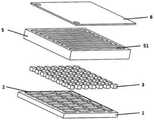
图2是本实用新型的一种一体化工作芯片/热电制冷芯片散热温控结构的分体示意图;Fig. 2 is a split schematic diagram of an integrated working chip/thermoelectric cooling chip heat dissipation temperature control structure of the present invention;
图3是一种一体化工作芯片/热电制冷芯片散热温控结构的一种典型应用分解图;Figure 3 is an exploded view of a typical application of an integrated working chip/thermoelectric cooling chip heat dissipation and temperature control structure;
图4是一种一体化工作芯片/热电制冷芯片散热温控结构的一种典型应用装配剖视图;4 is a cross-sectional view of a typical application assembly of an integrated working chip/thermoelectric cooling chip heat dissipation and temperature control structure;
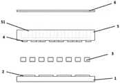
附图标记:1-工作芯片,2-第一电极层,3-热电颗粒层,4-第二电极层,5-微流控芯片流道层,51-微流道,6-微流控芯片盖板层,7-电路板,8-封装板。Reference signs: 1-working chip, 2-first electrode layer, 3-thermoelectric particle layer, 4-second electrode layer, 5-channel layer of microfluidic chip, 51-microfluidic channel, 6-microfluidic Chip cover layer, 7-circuit board, 8-package board.
具体实施方式Detailed ways
如图1-图2所示,本实用新型一体化工作芯片/热电制冷芯片散热温控结构,该结构包括:工作芯片1、第一电极层2、热电颗粒层3、第二电极层4、微流控芯片层(微流控芯片流道层5、微流控芯片盖板层6)或散热器层,具体结构如下:As shown in Figures 1 to 2, the integrated working chip/thermoelectric cooling chip heat dissipation and temperature control structure of the present invention includes: a working
第一电极层2位于工作芯片1顶部,第二电极层4位于微流控芯片层或散热器层底部。热电颗粒层3焊接在第一电极层2和第二电极层4之间,形成传统热电器件电串联、热并联结构。The
微流控芯片层包括微流控芯片流道层5、微流控芯片盖板层6,微流控芯片盖板层6安装于微流控芯片流道层5顶部,微流控芯片流道层5上设有微流道51,微流道结构为往复式平行排布型结构,微流控芯片盖板层6上有两个通孔:进水孔和出水孔,用于外接水路。使用时,在微流道51水路中加入一可调功率的水泵用于水循环。The microfluidic chip layer includes a microfluidic chip
其中,热电颗粒层3为N型和P型热电半导体材料(薄膜热电半导体材料或块体热电半导体材料),包括GeSi基合金、GeTe基合金、Bi2Te3基合金或Mg3Bi2基合金等。第一电极层2材料和第二电极层4材料可选择为Ti、Cu、Ni、Au、Cr、Nb、Ag等高导电导热金属构成的单层或两层以上的膜结构。第一电极层、热电颗粒层、第二电极层空间排列方式和电连接方式均与商用块体热电器件相同。微流控芯片流道层5为Si或SiN材料或Al2O3材料,微流控芯片盖板层6为Si或聚二甲基硅氧烷(PDMS)材料。散热器层可以为Si材料、AlN陶瓷材料、Al2O3陶瓷等高导热材料。The
在具体实施过程中,本实用新型一体化工作芯片/热电制冷芯片散热温控结构的集成方法包括:电极直接生长技术、热电颗粒切割及装配技术、热电制冷芯片焊接技术、深硅刻蚀技术、飞秒激光微流控加工技术,具体步骤如下:In the specific implementation process, the integrated method of the integrated working chip/thermoelectric refrigeration chip heat dissipation temperature control structure of the present invention includes: electrode direct growth technology, thermoelectric particle cutting and assembly technology, thermoelectric refrigeration chip welding technology, deep silicon etching technology, Femtosecond laser microfluidic processing technology, the specific steps are as follows:
(1)微流控芯片制备:采用飞秒激光刻蚀技术刻蚀Al2O3陶瓷或AlN陶瓷制备微流道,或采用深硅刻蚀技术刻蚀Si微流道。在微流道层Al2O3或AlN上物理沉积约20~500nmSiO2后,采用紫外臭氧处理技术处理PDMS,将PDMS与Al2O3或AlN对准加压,实现PDMS与Al2O3或AlN的化学键合;或采用Si晶圆键合技术直接键合Si盖板与Si微流道层。(1) Microfluidic chip preparation: microfluidic channels are prepared by etching Al2 O3 ceramics or AlN ceramics by femtosecond laser etching technology, or Si microfluidic channels are etched by deep silicon etching technology. After physical deposition of about 20-500 nm SiO2 on the micro-channel layer Al2 O3 or AlN, the PDMS is treated with ultraviolet ozone treatment technology, and the PDMS and Al2 O3 or AlN are aligned and pressurized to realize PDMS and Al2 O3 Or chemical bonding of AlN; or using Si wafer bonding technology to directly bond the Si cover plate and the Si microchannel layer.
(2)电极直接生长:在微流道层无微流道面和工作芯片某一面采用电镀或磁控溅射或电子束蒸发直接生长图案化电极。(2) Direct electrode growth: The patterned electrodes are directly grown by electroplating or magnetron sputtering or electron beam evaporation on the surface without microchannels in the microchannel layer and on one side of the working chip.
(3)热电颗粒切割及装配:利用点胶或丝网印刷术在第一电极层及第二电极层制备合金焊膏(如:AuSn、SnSb或SnBi等),利用图像识别及贴片技术在第一电极层上装配热电颗粒层。(3) Cutting and assembly of thermoelectric particles: Alloy solder paste (such as AuSn, SnSb or SnBi, etc.) is prepared on the first electrode layer and the second electrode layer by dispensing or screen printing, and image recognition and patch technology are used in the A layer of pyroelectric particles is assembled on the first electrode layer.
(4)热电制冷芯片焊接:利用图像识别及贴片技术将微流控层第二电极层与热电颗粒层顶部装配,在带有保护气氛(如:氮气、氩气或氦气等)的焊炉里焊接,其焊接参数与所使用的合金焊膏相对应。(4) Thermoelectric refrigeration chip welding: Using image recognition and patch technology to assemble the second electrode layer of the microfluidic layer and the top of the thermoelectric particle layer, in a welding with a protective atmosphere (such as nitrogen, argon or helium, etc.) Furnace soldering with soldering parameters corresponding to the alloy solder paste used.
下述实施例是为了更好地进一步理解本实用新型,并不局限于所述最佳实施方式,不对本实用新型的内容和保护范围构成限制,任何人在本实用新型的启示下或是将本实用新型与其他现有技术的特征进行组合而得出的任何与本实用新型相同或向近似的产品,均落在本实用新型的保护范围之内。The following examples are for a better understanding of the present utility model, are not limited to the best embodiment, do not limit the content and protection scope of the present utility model, anyone under the inspiration of the present utility model or will Any product identical or similar to the present utility model obtained by combining the features of the present utility model with other prior art features falls within the protection scope of the present utility model.
实施例中未注明具体实现步骤或条件者,按照本领域内文献所描述的常规试验步骤操作或条件即可进行。所用试剂或仪器未注明生产厂商这,均为可以通过市购获得的常规试剂产品。If the specific implementation steps or conditions are not indicated in the examples, it can be carried out according to the routine test steps operations or conditions described in the literature in this field. The reagents or instruments used are not indicated by the manufacturer, and they are all conventional reagent products that can be obtained from the market.
实施例1Example 1
如图1-图4所示,本实施例为一体化工作芯片/热电制冷芯片散热温控结构的一种典型应用,包括:工作芯片1、第一电极层2、热电颗粒层3、第二电极层4、微流控芯片流道层5、微流控芯片盖板层6、电路板7和封装板8,工作芯片1通过锡焊工艺与电路板7构成电连接,第一电极层2直接制作于工作芯片1顶部,第二电极层4直接制作于微流控芯片流道层5底部。热电颗粒层3通过焊接工艺焊接在第一电极层2和第二电极层4之间,形成传统热电器件电串联、热并联结构。封装板8与电路板7上下相对设置,且封装板8通过密封胶与电路板7粘接密封,封装板8的中间开设窗口,封装板8的窗口通过密封胶与微流控芯片流道层5的侧面粘接,微流控芯片盖板层6安装于微流控芯片流道层5顶部形成微流控芯片层。其中,工作芯片1、第一电极层2、热电颗粒层3、第二电极层4、微流控芯片流道层5、微流控芯片盖板层6均位于封装板8的窗口内,封装板8与电路板7之间的密封区域可以是空气、氩气、氮气或氦气。微流控芯片流道层5上设有微流道51,用于通冷却水,增大散热效果。其中,微流道51为往复式平行排布型结构,其尺寸为:微流道截面宽度10μm~500μm,微流道截面高度20μm~1mm。微流控芯片盖板层6上有两个通孔:进水孔和出水孔,用于外接水路。实际使用时,需要在微流道水路中加入一可调功率的水泵用于水循环。As shown in Figures 1 to 4, this embodiment is a typical application of the integrated working chip/thermoelectric cooling chip heat dissipation and temperature control structure, including: a working
本实施例中,热电颗粒层3采用N型Bi2Te3块体材料和P型Bi1.5Sb0.5Te3块体材料,其具体尺寸均为:长200μm,宽200μm,高200μm;第一电极层2为Au材料,第二电极层4为Au材料,微流控芯片流道层5为Si材料,微流控芯片盖板层6为Si材料。In this embodiment, the
本实施例的使用原理大致如下所述:The usage principle of this embodiment is roughly as follows:
本实施例制冷结构工作时,工作芯片1发出大量热量,给第二电极层4的两端施加电压,由于热电材料的帕尔贴效应,热量被搬运到微流控芯片流道层5。而微流控芯片流道层5中的微流道液体由于温度较低,吸收热量并被水泵抽走,从而实现工作芯片1的高效制冷。并且,通过调节施加电压的大小、水泵的功率,可以调节芯片的实际温度,从而实现芯片的精准控温。When the refrigeration structure of this embodiment works, the working
结果表明,本实用新型通过将热电制冷芯片直接集成在工作芯片上,大大降低了界面寄生热阻和电阻,极大地提高了散热效率。同时,结合微流道技术,保证热电制冷芯片的热端散热,进一步提升了散热性能。本实用新型所采用的封装技术均较容易实现并且与当下半导体器件制造工艺相兼容,有非常大的应用潜力。The results show that the utility model greatly reduces the interface parasitic thermal resistance and resistance by directly integrating the thermoelectric cooling chip on the working chip, and greatly improves the heat dissipation efficiency. At the same time, combined with the micro-channel technology, the heat dissipation of the hot end of the thermoelectric cooling chip is ensured, which further improves the heat dissipation performance. The packaging technology adopted by the present invention is relatively easy to implement and compatible with the current semiconductor device manufacturing process, and has very great application potential.
显然,上述实施例仅仅是为清楚地说明所做的举例,而并非对实施方式的限定。对于所属领域的普通技术人员来说,在上述说明的基础上还可以做出其它不同形式的变化或变动。这里无需也无法对所有的实施方式予以穷举。而由此所引申出的显而易见的变化或变动仍处于本实用新型创造的保护范围之中。Obviously, the above-mentioned embodiments are only examples for clear description, and are not intended to limit the implementation manner. For those of ordinary skill in the art, changes or modifications in other different forms can also be made on the basis of the above description. There is no need and cannot be exhaustive of all implementations here. And the obvious changes or changes derived from this are still within the protection scope of the present invention.
Claims (4)
Priority Applications (1)
| Application Number | Priority Date | Filing Date | Title |
|---|---|---|---|
| CN202220246236.3UCN217035624U (en) | 2022-01-30 | 2022-01-30 | Integrated working chip/thermoelectric refrigeration chip heat dissipation temperature control structure |
Applications Claiming Priority (1)
| Application Number | Priority Date | Filing Date | Title |
|---|---|---|---|
| CN202220246236.3UCN217035624U (en) | 2022-01-30 | 2022-01-30 | Integrated working chip/thermoelectric refrigeration chip heat dissipation temperature control structure |
Publications (1)
| Publication Number | Publication Date |
|---|---|
| CN217035624Utrue CN217035624U (en) | 2022-07-22 |
Family
ID=82449149
Family Applications (1)
| Application Number | Title | Priority Date | Filing Date |
|---|---|---|---|
| CN202220246236.3UActiveCN217035624U (en) | 2022-01-30 | 2022-01-30 | Integrated working chip/thermoelectric refrigeration chip heat dissipation temperature control structure |
Country Status (1)
| Country | Link |
|---|---|
| CN (1) | CN217035624U (en) |
Cited By (1)
| Publication number | Priority date | Publication date | Assignee | Title |
|---|---|---|---|---|
| WO2025030335A1 (en)* | 2023-08-07 | 2025-02-13 | 深圳市江波龙电子股份有限公司 | Temperature adjustment device and test device for integrated chip |
- 2022
- 2022-01-30CNCN202220246236.3Upatent/CN217035624U/enactiveActive
Cited By (1)
| Publication number | Priority date | Publication date | Assignee | Title |
|---|---|---|---|---|
| WO2025030335A1 (en)* | 2023-08-07 | 2025-02-13 | 深圳市江波龙电子股份有限公司 | Temperature adjustment device and test device for integrated chip |
Similar Documents
| Publication | Publication Date | Title |
|---|---|---|
| CN107170714B (en) | Low parasitic inductance power module and double-sided heat dissipation low parasitic inductance power module | |
| JP4754483B2 (en) | ELECTRONIC DEVICE USING NANOTUBE AREA AND SUPPORTING THERMAL HEAT SINK ACTION AND ITS MANUFACTURING METHOD | |
| JP7022901B2 (en) | Semiconductor laser device | |
| TWI295115B (en) | Encapsulation and methods thereof | |
| JP4594237B2 (en) | Semiconductor device | |
| CN105474418B (en) | Thermoelectric module and heat conversion device including the thermoelectric module | |
| WO2004061982A1 (en) | Cooling device for electronic component using thermo-electric conversion material | |
| JP2004140356A (en) | Power semiconductor module | |
| CN116564911A (en) | Integrated working chip/thermoelectric refrigeration chip heat dissipation temperature control structure and integration method | |
| WO2020248905A1 (en) | Wafer-level 3d stacked microchannel heat dissipation structure and manufacturing method therefor | |
| JP5503805B2 (en) | Electronic chip having a channel through which heat transporting refrigerant can flow, electronic component, and switching arm with built-in electronic chip | |
| CN113056087A (en) | Printed circuit board embedded with micro-channel and preparation method thereof | |
| CN217035624U (en) | Integrated working chip/thermoelectric refrigeration chip heat dissipation temperature control structure | |
| CN116546869A (en) | Novel micro-flow thermoelectric radiator, manufacturing method thereof and radiating method | |
| CN119584622B (en) | Semiconductor packaging structure and manufacturing method thereof, power device, and electronic device | |
| US20060068611A1 (en) | Heat transfer device and system and method incorporating same | |
| CN114207967B (en) | Double-sided cooling of laser diodes | |
| CN109037175A (en) | power device and its packaging method | |
| US11355419B2 (en) | Power semiconductor module | |
| US20070200223A1 (en) | Semiconductor device and semiconductor module therewith | |
| US20070053394A1 (en) | Cooling device using direct deposition of diode heat pump | |
| CN209418488U (en) | A Metal Microchannel Heat Sink Structure for Chip Heat Dissipation | |
| JP2002164585A (en) | Thermoelectric conversion module | |
| JP2001332773A (en) | Multi-layer substrate for thermoelectric module and method of manufacturing the same, and thermoelectric module using multi-layer substrate | |
| JP2001024125A (en) | Flat semiconductor element |
Legal Events
| Date | Code | Title | Description |
|---|---|---|---|
| GR01 | Patent grant | ||
| GR01 | Patent grant |