CN211698994U - Fingerprint sensing device - Google Patents
Fingerprint sensing deviceDownload PDFInfo
- Publication number
- CN211698994U CN211698994UCN202020701780.3UCN202020701780UCN211698994UCN 211698994 UCN211698994 UCN 211698994UCN 202020701780 UCN202020701780 UCN 202020701780UCN 211698994 UCN211698994 UCN 211698994U
- Authority
- CN
- China
- Prior art keywords
- switch
- coupled
- sensing
- amplifier
- capacitor
- Prior art date
- Legal status (The legal status is an assumption and is not a legal conclusion. Google has not performed a legal analysis and makes no representation as to the accuracy of the status listed.)
- Expired - Fee Related
Links
Images


Classifications
- G—PHYSICS
- G06—COMPUTING OR CALCULATING; COUNTING
- G06V—IMAGE OR VIDEO RECOGNITION OR UNDERSTANDING
- G06V40/00—Recognition of biometric, human-related or animal-related patterns in image or video data
- G06V40/10—Human or animal bodies, e.g. vehicle occupants or pedestrians; Body parts, e.g. hands
- G06V40/12—Fingerprints or palmprints
- G06V40/13—Sensors therefor
- G06V40/1318—Sensors therefor using electro-optical elements or layers, e.g. electroluminescent sensing
Landscapes
- Engineering & Computer Science (AREA)
- Human Computer Interaction (AREA)
- Physics & Mathematics (AREA)
- General Physics & Mathematics (AREA)
- Multimedia (AREA)
- Theoretical Computer Science (AREA)
- Image Input (AREA)
- Transforming Light Signals Into Electric Signals (AREA)
Abstract
Translated fromChinese
Description
Translated fromChinese技术领域technical field
本实用新型涉及一种感测装置,尤其涉及一种指纹感测装置。The utility model relates to a sensing device, in particular to a fingerprint sensing device.
背景技术Background technique
近年来,生物识别技术发展很快。由于安全码和访问卡很容易被盗或丢失,因此更多地关注指纹识别技术。指纹是唯一且不变的,并且每个人具有多个手指用于身份识别。另外,可以使用指纹传感器容易地取得指纹。因此,指纹识别可以提高安全性和便利性,并且可以更好地保护财务安全和保密数据。In recent years, biometric technology has developed rapidly. Since security codes and access cards can easily be stolen or lost, more attention has been paid to fingerprint recognition technology. Fingerprints are unique and immutable, and each person has multiple fingers for identification. In addition, a fingerprint can be easily acquired using a fingerprint sensor. Therefore, fingerprint recognition can improve security and convenience, and can better protect financial security and confidential data.
一般而言,光学式的指纹感测装置可包括由面板、光发射源、光准直器以及光电传感器所组成,通过光发射源提供照明光至按压在面板上的手指,再经由面板以及手指对象反射具有指纹信息的图像光,并且经由光准直器传递至光电传感器。由于光准直器所传递的图像光仅为反射光的一小部份,为了增加感测灵敏度与降低模块高度,对应一个感测像素,光准直器通常会配置多个透镜来传递图像光。如此虽可有效提高指纹感测的灵敏度,然由于需进行处理的信号数量变多,将大幅提高后续进行信号处理的装置对于数据处理速度的要求,例如需配置高速的模拟数字转换器,而具有大幅提高产品成本以及功率消耗的缺点。Generally speaking, an optical fingerprint sensing device may include a panel, a light emitting source, a light collimator, and a photoelectric sensor. The light emitting source provides illumination light to a finger pressing on the panel, and then passes through the panel and the finger. The object reflects the image light with the fingerprint information and passes it to the photosensor via the light collimator. Since the image light transmitted by the light collimator is only a small part of the reflected light, in order to increase the sensing sensitivity and reduce the height of the module, corresponding to one sensing pixel, the light collimator is usually equipped with multiple lenses to transmit the image light . Although this can effectively improve the sensitivity of fingerprint sensing, due to the increase in the number of signals to be processed, the requirements for the data processing speed of subsequent signal processing devices will be greatly increased, for example, a high-speed analog-to-digital converter needs to be configured. The disadvantages of greatly increasing product cost and power consumption.
实用新型内容Utility model content
本实用新型提供一种指纹感测装置,可有效降低生产成本,降低功率消耗。The utility model provides a fingerprint sensing device, which can effectively reduce production cost and power consumption.
本实用新型的指纹感测装置包括感测像素阵列、多个积分器电路以及增益放大器电路。感测像素阵列包括多个感测像素,各感测像素包括多个子感测像素,各子感测像素感测包括指纹信息的光信号而产生子感测信号。上述多个积分器电路耦接感测像素阵列,分别通过多条列信号线耦接对应的子感测像素,分批对上述多个子感测信号进行积分运算,以累加上述多个子感测信号的感测值而产生对应各感测像素的感测信号。各积分器电路包括第一放大器、第一电容以及开关及电容电路。第一放大器的正输入端耦接第一参考电压。第一电容耦接第一放大器的负输入端与对应的积分器电路的输出端之间。开关及电容电路包括第二电容,切换第二电容的连接状态而使对应的积分器电路周期性地进入电压设置期间与积分运算期间,其中开关及电容电路于电压设置期间,使第一放大器的输出端与负输入端相连接并断开第二电容与第一放大器的负输入端与输出端间的连接,并于积分运算期间使第二电容耦接于第一放大器的负输入端与输出端之间,以使对应的积分器电路执行积分运算。增益放大器电路耦接积分器电路,放大感测信号以产生放大信号。The fingerprint sensing device of the present invention includes a sensing pixel array, a plurality of integrator circuits and a gain amplifier circuit. The sensing pixel array includes a plurality of sensing pixels, each of the sensing pixels includes a plurality of sub-sensing pixels, and each of the sub-sensing pixels senses an optical signal including fingerprint information to generate a sub-sensing signal. The plurality of integrator circuits are coupled to the sensing pixel array, respectively coupled to the corresponding sub-sensing pixels through a plurality of column signal lines, and perform integral operations on the plurality of sub-sensing signals in batches to accumulate the plurality of sub-sensing signals A sensing signal corresponding to each sensing pixel is generated. Each integrator circuit includes a first amplifier, a first capacitor, and a switch and capacitor circuit. The positive input terminal of the first amplifier is coupled to the first reference voltage. The first capacitor is coupled between the negative input terminal of the first amplifier and the output terminal of the corresponding integrator circuit. The switch and capacitor circuit includes a second capacitor, and the connection state of the second capacitor is switched to cause the corresponding integrator circuit to periodically enter the voltage setting period and the integration operation period, wherein the switch and capacitor circuit make the first amplifier's power during the voltage setting period. The output terminal is connected to the negative input terminal, and the connection between the second capacitor and the negative input terminal and the output terminal of the first amplifier is disconnected, and the second capacitor is coupled to the negative input terminal and the output terminal of the first amplifier during the integration operation. between the terminals, so that the corresponding integrator circuit performs the integral operation. The gain amplifier circuit is coupled to the integrator circuit, and amplifies the sensing signal to generate an amplified signal.
在本实用新型的一实施例中,开关及电容电路还包括:第一开关,耦接于第二电容的一端与第一放大器的负输入端之间;以及第二开关,耦接于第二电容的另一端与第一放大器的输出端之间,第一开关与第二开关于各个积分运算期间结束后进入电压设置期间前进入断开状态。In an embodiment of the present invention, the switch and capacitor circuit further includes: a first switch coupled between one end of the second capacitor and the negative input end of the first amplifier; and a second switch coupled to the second Between the other end of the capacitor and the output end of the first amplifier, the first switch and the second switch enter the disconnected state after each integral operation period ends and before entering the voltage setting period.
在本实用新型的一实施例中,第一开关早于第二开关进入断开状态。In an embodiment of the present invention, the first switch enters the off state earlier than the second switch.
在本实用新型的一实施例中,各积分器电路还包括:第三开关,耦接第一放大器的负输入端与输出端之间,于电压设置期间处于导通状态,于积分运算期间处于断开状态。In an embodiment of the present invention, each integrator circuit further includes: a third switch, coupled between the negative input terminal and the output terminal of the first amplifier, is in a conducting state during the voltage setting period, and is in a conducting state during the integration operation period disconnected state.
在本实用新型的一实施例中,第一开关与第二开关于各感测像素的第一个电压设置期间处于导通状态,并于各感测像素的其余电压设置期间处于断开状态。In an embodiment of the present invention, the first switch and the second switch are in an on state during the first voltage setting period of each sensing pixel, and are in an off state during the remaining voltage setting periods of each sensing pixel.
在本实用新型的一实施例中,增益放大器电路,包括:第二放大器,其正输入端耦接第二参考电压;第三电容,耦接于多个积分器电路的输出端与第二放大器的正输入端之间;以及第四电容,耦接于第二放大器的负输入端与输出端之间。In an embodiment of the present invention, the gain amplifier circuit includes: a second amplifier, whose positive input terminal is coupled to the second reference voltage; a third capacitor, which is coupled to the output terminals of the multiple integrator circuits and the second amplifier between the positive input end of the second amplifier; and a fourth capacitor, coupled between the negative input end and the output end of the second amplifier.
在本实用新型的一实施例中,各积分器电路还包括:第一开关,耦接于积分器电路的输出端与所增益放大器电路的输入端之间,受控于列选择信号而输出感测信号。In an embodiment of the present invention, each integrator circuit further includes: a first switch, coupled between the output end of the integrator circuit and the input end of the gain amplifier circuit, controlled by the column selection signal to output a sense of measurement signal.
在本实用新型的一实施例中,增益放大器电路还包括:第二开关,耦接于第二放大器的负输入端与输出端之间,与第一开关同时导通,早于第一开关进入断开状态。In an embodiment of the present invention, the gain amplifier circuit further includes: a second switch, coupled between the negative input terminal and the output terminal of the second amplifier, turned on at the same time as the first switch, and entered earlier than the first switch. disconnected state.
在本实用新型的一实施例中,各积分器电路还包括:In an embodiment of the present invention, each integrator circuit further includes:
第三开关,耦接于第一放大器的负输入端与输出端之间,于第二开关断开后且第一开关断开前进入导通状态。The third switch, coupled between the negative input terminal and the output terminal of the first amplifier, enters a conducting state after the second switch is turned off and before the first switch is turned off.
在本实用新型的一实施例中,各子感测像素包括:光电转换单元,转换光信号而产生光电转换信号;传输晶体管,其第一端耦接光电转换单元,受控于传输控制信号而输出光电转换信号;重置晶体管,其第一端耦接操作电压,重置晶体管的第二端耦接传输晶体管的第二端,重置晶体管受控于重置控制信号而重置传输晶体管的第二端的电压;放大晶体管,其控制端耦接传输晶体管的第二端,放大晶体管的第一端耦接操作电压,反应光电转换信号的电压值而产生子感测信号;以及选择晶体管,耦接于放大晶体管的第二端与对应的积分器电路的输入端,受控于选择控制信号而将子感测信号输出至对应的积分器电路。In an embodiment of the present invention, each sub-sensing pixel includes: a photoelectric conversion unit, which converts a light signal to generate a photoelectric conversion signal; a transmission transistor, the first end of which is coupled to the photoelectric conversion unit, and is controlled by the transmission control signal to generate a photoelectric conversion signal. outputting a photoelectric conversion signal; a reset transistor, the first end of which is coupled to the operating voltage, the second end of the reset transistor is coupled to the second end of the transfer transistor, and the reset transistor is controlled by the reset control signal to reset the transfer transistor the voltage of the second terminal; the amplifying transistor, the control terminal of which is coupled to the second terminal of the transmission transistor, the first terminal of the amplifying transistor is coupled to the operating voltage, and generates the sub-sensing signal in response to the voltage value of the photoelectric conversion signal; and the selection transistor, which is coupled to The second terminal connected to the amplifying transistor and the input terminal of the corresponding integrator circuit is controlled by the selection control signal to output the sub-sensing signal to the corresponding integrator circuit.
基于上述,本实用新型实施例的积分器电路可分批对多个子感测信号进行积分运算,以累加多个子感测信号的感测值而产生对应各感测像素的感测信号,如此可有效减少后级电路需进行处理的感测信号数量,而可不需配置具有高处理速度的电路,进而有效降低产品成本以及功率消耗。Based on the above, the integrator circuit of the embodiment of the present invention can perform an integral operation on a plurality of sub-sensing signals in batches, so as to accumulate the sensing values of the plurality of sub-sensing signals to generate a sensing signal corresponding to each sensing pixel. The number of sensing signals to be processed by the post-stage circuit is effectively reduced, and a circuit with high processing speed is not required, thereby effectively reducing product cost and power consumption.
为让本实用新型的上述特征和优点能更明显易懂,下文特举实施例,并配合附图作详细说明如下。In order to make the above-mentioned features and advantages of the present utility model more obvious and easy to understand, the following examples are given and described in detail in conjunction with the accompanying drawings as follows.
附图说明Description of drawings
图1是依照本实用新型的实施例的一种指纹感测装置的示意图;1 is a schematic diagram of a fingerprint sensing device according to an embodiment of the present invention;
图2是依照本实用新型另一实施例的一种指纹感测装置的示意图;2 is a schematic diagram of a fingerprint sensing device according to another embodiment of the present invention;
图3是依照本实用新型的实施例的指纹感测装置的信号的波形图。3 is a waveform diagram of a signal of a fingerprint sensing device according to an embodiment of the present invention.
具体实施方式Detailed ways
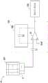
图1是依照本实用新型的实施例的一种指纹感测装置的示意图,请参照图1。指纹感测装置包括感测像素P1、积分器电路102以及增益放大器电路104,其中积分器电路102耦接感测像素P1与增益放大器电路104。值得注意的是,指纹感测装置所包括的感测像素P1以及积分器电路102的数量并不以图1为限,举例来说,指纹感测装置可包括由多个感测像素P1形成的感测像素阵列以及多个积分器电路102,各个感测像素P1可分别与对应的积分器电路102耦接,为简化说明本实施例仅以一个感测像素P1以及一个积分器电路102为例进行说明。FIG. 1 is a schematic diagram of a fingerprint sensing device according to an embodiment of the present invention, please refer to FIG. 1 . The fingerprint sensing device includes a sensing pixel P1 , an
如图1所示,感测像素P1可包括多个子感测像素SP1,子感测像素SP1可形成子感测像素阵列,例如8×8的子感测像素阵列,然不以此为限。各子感测像素SP1可感测包括指纹信息的光信号而产生子感测信号。积分器电路102可通过多条列信号线L1耦接子感测像素SP1,而分批对多个子感测信号进行积分运算。例如积分器电路102可一次对一行子感测像素SP1进行积分运算,待完成各行的子感测像素SP1的积分运算后,亦即完成感测像素P1的积分运算后,再将累计的积分结果传送给增益放大器电路104进行信号放大处理,以产生放大信号给后级电路进行信号转换与分析处理。As shown in FIG. 1 , the sensing pixel P1 may include a plurality of sub-sensing pixels SP1, and the sub-sensing pixels SP1 may form a sub-sensing pixel array, such as an 8×8 sub-sensing pixel array, but not limited thereto. Each sub-sensing pixel SP1 can sense an optical signal including fingerprint information to generate a sub-sensing signal. The
进一步来说,积分器电路102可例如包括放大器A1、电容C1以及开关及电容电路106,其中电容C1耦接于放大器A1的负输入端与积分器电路104之间,放大器A1的正输入端耦接参考电压Vref1,开关级电容电路106可包括电容C2,电容C2耦接于放大器A1的负输入端与输出端之间。开关级电容电路106可切换电容C2的连接状态而使积分器电路102周期性地进入电压设置期间与积分运算期间,其中开关及电容电路106于电压设置期间,使放大器A1的输出端与负输入端相连接并断开电容C2与放大器A1的负输入端与输出端间的连接,并于积分运算期间使电容C2耦接于放大器A1的负输入端与输出端之间,以使对应的积分器电路执行积分运算。如此在电压设置期间可重置电容C1上的电压而不会影响电容C2所储存的指纹信息,且可使电容C2累计在积分运算期间所接收的指纹信息,待完成感测像素P1中各个子感测像素SP1的积分运算后,再将积分结果传送给增益放大器电路104。如此可不需如现有技术般配置具有高数据处理速度的后级电路(例如高处理速度的模拟数字转换器)来逐行地处理各行子感测像素SP1的积分结果,因此可有效降低指纹感测装置的生产成本,降低功率消耗。Further, the
图2是依照本实用新型另一实施例的一种指纹感测装置的示意图,请参照图1。在本实施例中,为简化说明,以单一个子感测像素SP1来说明指纹感测装置的实施方式。如图2所示,子感测像素SP1可包括光电转换单元D1、传输晶体管M1、重置晶体管M2、放大晶体管M3以及选择晶体管M4其中光电转换单元D1可例如为光电二极管,其阴极与阳极分别耦接传输晶体管M1的第一端与接地,传输晶体管M1的第二端耦接放大晶体管M3的控制端,传输晶体管M1的控制端接收传输控制信号TG。重置晶体管M2耦接于操作电压Vdd与放大晶体管M3的控制端之间,重置晶体管M2的控制端接收重置控制信号RST。放大晶体管M3的第一端与第二端分别耦接操作电压Vdd与选择晶体管M4的第一端,选择晶体管M4的第二端耦接电容C1与一电流源I1,选择晶体管M4的控制端则耦接选择控制信号RSEL。FIG. 2 is a schematic diagram of a fingerprint sensing device according to another embodiment of the present invention, please refer to FIG. 1 . In this embodiment, to simplify the description, a single sub-sensing pixel SP1 is used to describe the implementation of the fingerprint sensing device. As shown in FIG. 2 , the sub-sensing pixel SP1 may include a photoelectric conversion unit D1, a transfer transistor M1, a reset transistor M2, an amplifying transistor M3, and a selection transistor M4, wherein the photoelectric conversion unit D1 may be, for example, a photodiode, and its cathode and anode are respectively The first terminal of the transmission transistor M1 is coupled to ground, the second terminal of the transmission transistor M1 is coupled to the control terminal of the amplifying transistor M3, and the control terminal of the transmission transistor M1 receives the transmission control signal TG. The reset transistor M2 is coupled between the operating voltage Vdd and the control terminal of the amplifying transistor M3, and the control terminal of the reset transistor M2 receives the reset control signal RST. The first end and the second end of the amplifying transistor M3 are respectively coupled to the operating voltage Vdd and the first end of the selection transistor M4, the second end of the selection transistor M4 is coupled to the capacitor C1 and a current source I1, and the control end of the selection transistor M4 is is coupled to the selection control signal RSEL.
此外,积分器电路102的开关级电容电路106包括开关SW1~SW5与电容C2,开关SW1耦接于放大器A1的负输入端与电容C2之间,开关SW2耦接于放大器A1的输出端与电容C2之间,开关SW3以及SW4耦接于放大器A1的负输入端与输出端之间,开关SW5耦接于放大器A1的输出端与增益放大器电路104的输入端之间。另外,增益放大器电路104包括开关SW6、电容CC1、CC2以及放大器A2,电容CC1耦接于放大器A2的负输入端与开关SW5之间,放大器A2的正输入端耦接参考电压Vref2,开关SW6与电容C2耦接于放大器A2的负输入端与输出端之间。In addition, the switched
图3是依照本实用新型的实施例的指纹感测装置的信号的波形图,在图3中,RSEL<n>、RST<n>以及TG<n>分别代表第n行子感测像素SP1所对应的选择控制信号RSEL、重置控制信号RST以及传输控制信号TG,CS<m>则代表第m列感测像素P1所对应的列选择信号CS,以下以选择控制信号RSEL、重置控制信号RST、传输控制信号TG以及列选择信号CS说明第m列的感测像素P1中第n行子感测像素SP1的子感测信号的处理方式,其中m、n为正整数,在本实施例中n的最大值为8,然不以此为限,请同时参照图2与图3。如图3所示,重置晶体管M2可受控于重置控制信号RST而依据操作电压重置放大晶体管M3的控制端的电压,此时开关SW3受控于控制信号AZ而于电压设置期间TR导通,以重置电容C1的电压。当子感测像素SP1的所在行被选择以输出子感测信号时,选择晶体管M4可受控于选择控制信号RSEL而被导通,而后传输晶体管M1受控于传输控制信号而被导通,以将光电转换单元D1转换包括指纹信息的光信号所得到光电转换信号传送至放大晶体管M3的控制端,以使放大晶体管M3依据光电转换信号改变其导通程度,进而将指纹信息通过选择晶体管M4传送至电容C1。此时,开关SW1与SW2受控于控制信号INTP与INT于积分运算期间T1进入导通状态,以进行积分运算,而将指纹信息储存至电容C2中,于积分运算期间T1开关SW3受控于控制信号AZ而处于断开状态。3 is a waveform diagram of a signal of a fingerprint sensing device according to an embodiment of the present invention. In FIG. 3 , RSEL<n>, RST<n> and TG<n> represent the n-th row of sub-sensing pixels SP1, respectively The corresponding selection control signal RSEL, reset control signal RST, and transmission control signal TG, CS<m> represents the column selection signal CS corresponding to the m-th column of sensing pixels P1, and the selection control signal RSEL, reset control hereinafter The signal RST, the transmission control signal TG, and the column selection signal CS describe the processing method of the sub-sensing signal of the sub-sensing pixel SP1 of the n-th row in the sensing pixel P1 of the m-th column, wherein m and n are positive integers. In the example, the maximum value of n is 8, but it is not limited to this. Please refer to FIG. 2 and FIG. 3 at the same time. As shown in FIG. 3 , the reset transistor M2 can be controlled by the reset control signal RST to reset the voltage of the control terminal of the amplifying transistor M3 according to the operating voltage. At this time, the switch SW3 is controlled by the control signal AZ to conduct TR during the voltage setting period. on to reset the voltage of capacitor C1. When the row of the sub-sensing pixel SP1 is selected to output the sub-sensing signal, the selection transistor M4 is controlled by the selection control signal RSEL to be turned on, and then the transfer transistor M1 is controlled by the transmission control signal to be turned on, The photoelectric conversion signal obtained by converting the optical signal including the fingerprint information by the photoelectric conversion unit D1 is transmitted to the control terminal of the amplifying transistor M3, so that the amplifying transistor M3 changes its degree of conduction according to the photoelectric conversion signal, and then the fingerprint information is passed through the selection transistor M4. sent to capacitor C1. At this time, the switches SW1 and SW2 are controlled by the control signals INTP and INT to enter the conducting state during the integration operation period T1 to perform the integration operation, and store the fingerprint information in the capacitor C2. During the integration operation period T1, the switch SW3 is controlled by the The control signal AZ is turned off.
值得注意的是,在各个感测像素P1第一次进入电压设置期间TR时,亦即第一次对电容C1的电压进行重置时,开关SW1与SW2也受控于控制信号INTP与INT进入导通状态,以将储存于电容C2中的上个感测像素P1的指纹信息消除。也就是说,在各个感测像素P1的子感测信号的信号处理期间,除了第一个电压设置期间TR以外,在其余的电压设置期间TR开关SW1与SW2皆处于断开的状态,如此可避免累计的积分结果被重置。此外,开关SW1与SW2各个积分运算期间TR结束后进入下一电压设置期间T1前进入断开状态,以避免电容C2在下一电压设置期间T1被重置,在本实施例中,可使开关SW1早于开关SW2进入断开状态,由于开关SW1耦接至放大器A1的负输入端,而放大器A1的负输入端具有虚拟接地的特性,因此先断开开关SW1,可避免电容C2所储存的指纹信息受到开关SW1的切换动作影响而失真。It is worth noting that when each sensing pixel P1 enters the voltage setting period TR for the first time, that is, when the voltage of the capacitor C1 is reset for the first time, the switches SW1 and SW2 are also controlled by the control signals INTP and INT to enter In the on state, the fingerprint information of the last sensing pixel P1 stored in the capacitor C2 is eliminated. That is to say, during the signal processing period of the sub-sensing signal of each sensing pixel P1, except for the first voltage setting period TR, the switches SW1 and SW2 are both turned off in the remaining voltage setting periods TR. To avoid the accumulated points result being reset. In addition, the switches SW1 and SW2 enter the off state after each integral operation period TR ends and before entering the next voltage setting period T1 to prevent the capacitor C2 from being reset during the next voltage setting period T1. In this embodiment, the switch SW1 can be Before the switch SW2 enters the off state, since the switch SW1 is coupled to the negative input terminal of the amplifier A1, and the negative input terminal of the amplifier A1 has the characteristics of virtual ground, the switch SW1 is turned off first to avoid the fingerprint stored in the capacitor C2. The information is distorted by the switching operation of the switch SW1.
在完成感测像素P1中各行子感测像素SP1的积分运算后,开关SW5受控于列选择信号CS而被导通,同时开关SW6也受控于控制信号CK1而被导通,以重置电容CC1与CC2的电压。而后开关SW6受控于控制信号CK1而被断开,开关SW5则晚于开关SW6进入断开状态,开关SW4受控于控制信号EQ而在开关SW6断开后、开关SW5断开前进入导通状态,以将放大器A1的负输入端的电压(其包括累计的积分结果,亦即感测像素P1感测光信号所得到的感测信号)传送至电容CC1,以进行信号放大处理,而于放大器A2的输出端输出放大信号给后级电路进行信号转换与分析处理。开关SW4进入断开状态的时间点可例如为开关SW6下次进入导通状态前,亦即在增益放大器电路104进行另一感测像素P1的感测信号的信号放大处理前,开关SW4进入断开状态。After the integration operation of each row of sub-sensing pixels SP1 in the sensing pixel P1 is completed, the switch SW5 is controlled by the column selection signal CS to be turned on, and the switch SW6 is also controlled by the control signal CK1 to be turned on to reset Voltage on capacitors CC1 and CC2. Then the switch SW6 is controlled by the control signal CK1 to be turned off, the switch SW5 is turned off later than the switch SW6, and the switch SW4 is controlled by the control signal EQ to be turned on after the switch SW6 is turned off and before the switch SW5 is turned off. In this state, the voltage of the negative input terminal of the amplifier A1 (which includes the accumulated integration result, that is, the sensing signal obtained by sensing the light signal sensed by the sensing pixel P1 ) is transmitted to the capacitor CC1 for signal amplification processing. The output end of A2 outputs the amplified signal to the post-stage circuit for signal conversion and analysis processing. The time point when the switch SW4 enters the OFF state may be, for example, before the switch SW6 enters the ON state next time, that is, before the
综上所述,本实用新型实施例的积分器电路可分批对多个子感测信号进行积分运算,以累加多个子感测信号的感测值而产生对应各感测像素的感测信号,如此可有效减少后级电路需进行处理的感测信号数量,而可不需配置具有高处理速度的电路,进而有效降低产品成本以及功率消耗。To sum up, the integrator circuit of the embodiment of the present invention can perform an integral operation on a plurality of sub-sensing signals in batches, so as to accumulate the sensing values of the plurality of sub-sensing signals to generate a sensing signal corresponding to each sensing pixel, In this way, the number of sensing signals to be processed by the post-stage circuit can be effectively reduced, and a circuit with a high processing speed is not required, thereby effectively reducing product cost and power consumption.
虽然本实用新型已以实施例揭示如上,然其并非用以限定本实用新型,任何所属技术领域中技术人员,在不脱离本实用新型的精神和范围内,当可作些许的更改与润饰,故本实用新型的保护范围当视权利要求所界定的为准。Although the present utility model has been disclosed above with examples, it is not intended to limit the present utility model. Any person skilled in the art can make some changes and modifications without departing from the spirit and scope of the present utility model. Therefore, the protection scope of the present invention should be determined by the claims.
Claims (10)
Applications Claiming Priority (2)
| Application Number | Priority Date | Filing Date | Title |
|---|---|---|---|
| US201962887691P | 2019-08-16 | 2019-08-16 | |
| US62/887,691 | 2019-08-16 |
Publications (1)
| Publication Number | Publication Date |
|---|---|
| CN211698994Utrue CN211698994U (en) | 2020-10-16 |
Family
ID=71222941
Family Applications (2)
| Application Number | Title | Priority Date | Filing Date |
|---|---|---|---|
| CN202020701780.3UExpired - Fee RelatedCN211698994U (en) | 2019-08-16 | 2020-04-30 | Fingerprint sensing device |
| CN202010361695.1APendingCN111382728A (en) | 2019-08-16 | 2020-04-30 | Fingerprint Sensing Device |
Family Applications After (1)
| Application Number | Title | Priority Date | Filing Date |
|---|---|---|---|
| CN202010361695.1APendingCN111382728A (en) | 2019-08-16 | 2020-04-30 | Fingerprint Sensing Device |
Country Status (4)
| Country | Link |
|---|---|
| US (1) | US20220335746A1 (en) |
| CN (2) | CN211698994U (en) |
| TW (1) | TWI733427B (en) |
| WO (1) | WO2021031612A1 (en) |
Cited By (2)
| Publication number | Priority date | Publication date | Assignee | Title |
|---|---|---|---|---|
| CN111382728A (en)* | 2019-08-16 | 2020-07-07 | 神盾股份有限公司 | Fingerprint Sensing Device |
| CN113508577A (en)* | 2021-06-03 | 2021-10-15 | 曜芯科技有限公司 | Pixel array and related image sensor, fingerprint detection chip and electronic device |
Families Citing this family (1)
| Publication number | Priority date | Publication date | Assignee | Title |
|---|---|---|---|---|
| TWI783639B (en)* | 2020-12-22 | 2022-11-11 | 神盾股份有限公司 | Sensing apparatus and sensing method thereof |
Family Cites Families (22)
| Publication number | Priority date | Publication date | Assignee | Title |
|---|---|---|---|---|
| NO324029B1 (en)* | 2004-09-23 | 2007-07-30 | Thin Film Electronics Asa | Reading method and detection device |
| CN100555873C (en)* | 2006-08-24 | 2009-10-28 | 凌阳科技股份有限公司 | Programmable Gain Amplifier |
| US20120090757A1 (en)* | 2010-10-18 | 2012-04-19 | Qualcomm Mems Technologies, Inc. | Fabrication of touch, handwriting and fingerprint sensor |
| US8917387B1 (en)* | 2014-06-05 | 2014-12-23 | Secugen Corporation | Fingerprint sensing apparatus |
| KR102294778B1 (en)* | 2014-09-24 | 2021-08-30 | 삼성전자주식회사 | Touch sensing device |
| US9380208B1 (en)* | 2015-04-13 | 2016-06-28 | Omnivision Technologies, Inc. | Image sensor power supply rejection ratio noise reduction through ramp generator |
| CN107580709B (en)* | 2015-06-18 | 2021-02-12 | 深圳市汇顶科技股份有限公司 | Multifunctional fingerprint sensor with optical sensing capability |
| KR101685077B1 (en)* | 2015-08-18 | 2016-12-09 | 연세대학교 산학협력단 | gain-linearized pixel merged open loop pre-amplifier for small pixel |
| CN206451196U (en)* | 2016-08-17 | 2017-08-29 | 江西亿科光电有限公司 | A kind of fingerprint identification module |
| WO2018058336A1 (en)* | 2016-09-27 | 2018-04-05 | 深圳市汇顶科技股份有限公司 | Capacitive sensing circuit |
| EP3440594A4 (en)* | 2017-01-04 | 2019-09-25 | Shenzhen Goodix Technology Co., Ltd. | ENHANCING OPTICAL DETECTION PERFORMANCE OF OPTICAL SENSOR MODULE SUB-SCREEN FOR DIGITAL FOOTPRINT DETECTION ON SCREEN |
| CN109791325B (en)* | 2017-03-07 | 2022-02-08 | 深圳市汇顶科技股份有限公司 | Device with peripheral taskbar display and LCD underscreen optical sensor module for on-screen fingerprint sensing |
| CN107180611A (en)* | 2017-06-23 | 2017-09-19 | 京东方科技集团股份有限公司 | Fingerprint recognition and pixel-driving circuit and the display device with the circuit |
| US11734944B2 (en)* | 2017-08-03 | 2023-08-22 | Himax Technologies Limited | Display device with embedded biometric detection function in active region |
| CN107980142B (en)* | 2017-11-01 | 2021-07-20 | 深圳市汇顶科技股份有限公司 | Fingerprint identification circuit, fingerprint sensor and mobile terminal |
| KR102509610B1 (en)* | 2017-11-08 | 2023-03-14 | 삼성디스플레이 주식회사 | Fingerprint sensor and display device including the same |
| KR20190085657A (en)* | 2018-01-11 | 2019-07-19 | 삼성전자주식회사 | Fingerprint sensor and operation method thereof |
| CN110032918B (en)* | 2018-01-12 | 2022-01-11 | 京东方科技集团股份有限公司 | Fingerprint identification device, manufacturing method thereof and electronic device |
| TWI652625B (en)* | 2018-03-16 | 2019-03-01 | 友達光電股份有限公司 | Fingerprint sensing device |
| KR102761617B1 (en)* | 2018-12-26 | 2025-02-03 | 애플 인크. | Optical-fingerprint detection system |
| US10861885B1 (en)* | 2019-05-27 | 2020-12-08 | Novatek Microelectronics Corp. | Method of obtaining image data and related image sensing system |
| CN211698994U (en)* | 2019-08-16 | 2020-10-16 | 神盾股份有限公司 | Fingerprint sensing device |
- 2020
- 2020-04-30CNCN202020701780.3Upatent/CN211698994U/ennot_activeExpired - Fee Related
- 2020-04-30TWTW109114453Apatent/TWI733427B/ennot_activeIP Right Cessation
- 2020-04-30WOPCT/CN2020/088080patent/WO2021031612A1/ennot_activeCeased
- 2020-04-30CNCN202010361695.1Apatent/CN111382728A/enactivePending
- 2020-04-30USUS17/634,245patent/US20220335746A1/ennot_activeAbandoned
Cited By (3)
| Publication number | Priority date | Publication date | Assignee | Title |
|---|---|---|---|---|
| CN111382728A (en)* | 2019-08-16 | 2020-07-07 | 神盾股份有限公司 | Fingerprint Sensing Device |
| CN113508577A (en)* | 2021-06-03 | 2021-10-15 | 曜芯科技有限公司 | Pixel array and related image sensor, fingerprint detection chip and electronic device |
| CN113508577B (en)* | 2021-06-03 | 2024-03-05 | 汇顶科技私人有限公司 | Pixel array, related image sensor, fingerprint detection chip and electronic device |
Also Published As
| Publication number | Publication date |
|---|---|
| CN111382728A (en) | 2020-07-07 |
| WO2021031612A1 (en) | 2021-02-25 |
| TWI733427B (en) | 2021-07-11 |
| TW202109367A (en) | 2021-03-01 |
| US20220335746A1 (en) | 2022-10-20 |
Similar Documents
| Publication | Publication Date | Title |
|---|---|---|
| CN211698994U (en) | Fingerprint sensing device | |
| TWI757806B (en) | Fingerprint sensing apparatus | |
| US12250467B2 (en) | Event detecting device including an event signal generator and an output signal generator configured to generate an output signal by combining event signals | |
| CN110008860B (en) | Fingerprint identification framework and touch panel | |
| TWI793750B (en) | Capacitive fingerprint sensing device | |
| TWI718878B (en) | Optical fingerprint sensing apparatus | |
| TWI752654B (en) | Image sensing circuit and method | |
| CN109002218A (en) | A kind of display panel and its driving method, display device | |
| US11244139B2 (en) | Fingerprint recognition integrated circuit and fingerprint recognition device including the same | |
| CN111741240B (en) | Image sensors, fingerprint detection devices, and electronic equipment | |
| WO2020006753A1 (en) | Data compression method and apparatus | |
| CN215647069U (en) | Image sensing device | |
| CN112183320B (en) | Fingerprint recognition method, fingerprint recognition device and fingerprint recognition display device | |
| TW202324056A (en) | Fingerprint image generation method and device for saving memory | |
| TWI751849B (en) | Image sensing apparatus | |
| CN118057493A (en) | Fingerprint identification device, fingerprint identification method and moire image generation method | |
| US12026969B2 (en) | Fingerprint recognition device, readout circuit and operating method of fingerprint recognition device | |
| CN114205488A (en) | Image sensing circuit, image sensor, and method for driving image sensing circuit | |
| TWI718667B (en) | Optical fingerprint collection method and optical fingerprint sensing device and handheld device using the same | |
| TWI783639B (en) | Sensing apparatus and sensing method thereof | |
| TWI732400B (en) | Biological characteristic collection circuit and method, information processing device with the circuit, and information processing device using the method | |
| CN221829007U (en) | Signal processing circuits and electronic devices | |
| CN115761824A (en) | Fingerprint identification module, fingerprint identification method and device | |
| CN112135014A (en) | Signal acquisition device | |
| TW202125322A (en) | Biometric acquisition circuit and method, information processing device having the circuit, and information processing device applying the method wherein the biometric acquisition circuit includes a charge sampling unit, a linear amplifying unit, an analog-to-digital conversion unit, a signal processing unit, and a logarithmic amplification unit |
Legal Events
| Date | Code | Title | Description |
|---|---|---|---|
| GR01 | Patent grant | ||
| GR01 | Patent grant | ||
| CF01 | Termination of patent right due to non-payment of annual fee | Granted publication date:20201016 | |
| CF01 | Termination of patent right due to non-payment of annual fee |