CN211481600U - Circuit board assembly and electronic equipment - Google Patents
Circuit board assembly and electronic equipmentDownload PDFInfo
- Publication number
- CN211481600U CN211481600UCN201922120143.7UCN201922120143UCN211481600UCN 211481600 UCN211481600 UCN 211481600UCN 201922120143 UCN201922120143 UCN 201922120143UCN 211481600 UCN211481600 UCN 211481600U
- Authority
- CN
- China
- Prior art keywords
- circuit board
- electronic component
- groove
- board assembly
- height
- Prior art date
- Legal status (The legal status is an assumption and is not a legal conclusion. Google has not performed a legal analysis and makes no representation as to the accuracy of the status listed.)
- Active
Links
Images


Landscapes
- Telephone Set Structure (AREA)
Abstract
Description
Translated fromChinese技术领域technical field
本申请涉及电子设备技术领域,特别涉及一种电路板组件及电子设备。The present application relates to the technical field of electronic equipment, and in particular, to a circuit board assembly and electronic equipment.
背景技术Background technique
随着手机的功能越来越丰富,传统手机的电路板上设置的电子元器件(例如,电池管理芯片、基带芯片、射频收发芯片、电容或者电感)也越来越多。此时,传统手机的电路板的面积在不断的增大,而这将不利于传统手机的小型化设置。As the functions of mobile phones become more and more abundant, more and more electronic components (for example, battery management chips, baseband chips, radio frequency transceiver chips, capacitors or inductors) are provided on circuit boards of traditional mobile phones. At this time, the area of the circuit board of the traditional mobile phone is constantly increasing, which is not conducive to the miniaturization of the traditional mobile phone.
实用新型内容Utility model content
本申请提供一种面积较小的电路板组件及电子设备。The present application provides a circuit board assembly and an electronic device with a smaller area.
第一方面,本申请提供一种电路板组件。所述电路板组件包括第一电路板、第二电路板、第一电子元器件和第二电子元器件。所述第二电路板的第一板面连接所述第一电路板。可以理解的是,连接包括可拆卸连接以及不可拆卸连接。所述第二电路板设有第一凹槽及第二凹槽。所述第一凹槽的开口位于所述第一板面。所述第二凹槽的开口位于所述第一板面。在所述第二电路板的垂直方向上,所述第一凹槽的深度小于所述第二凹槽的深度。所述第一电子元器件与所述第二电子元器件均固定于所述第一电路板。所述第一电子元器件位于所述第一凹槽。所述第二电子元器件位于所述第二凹槽。在所述第二电路板的垂直方向上,所述第一电子元器件的高度小于所述第二电子元器件的高度。In a first aspect, the present application provides a circuit board assembly. The circuit board assembly includes a first circuit board, a second circuit board, a first electronic component and a second electronic component. The first board surface of the second circuit board is connected to the first circuit board. It can be understood that the connection includes detachable connection as well as non-detachable connection. The second circuit board is provided with a first groove and a second groove. The opening of the first groove is located on the first board surface. The opening of the second groove is located on the first board surface. In the vertical direction of the second circuit board, the depth of the first groove is smaller than the depth of the second groove. Both the first electronic component and the second electronic component are fixed on the first circuit board. The first electronic component is located in the first groove. The second electronic component is located in the second groove. In the vertical direction of the second circuit board, the height of the first electronic component is smaller than the height of the second electronic component.
在本实现方式中,通过将高度较低的所述第一电子元器件位于深度较浅的所述第一凹槽内,将高度较高的所述第二电子元器件位于深度较深的所述第二凹槽,从而既可以避免所述第二电路板因开设的凹槽较大而降低所述第二电路板的整体强度,又可以使得所述第一凹槽的空间与所述第二凹槽的空间能够得到有效地利用,也即显著提高所述第一凹槽与所述第二凹槽的空间利用率。In this implementation manner, by locating the first electronic component with a lower height in the first groove with a shallower depth, the second electronic component with a higher height is located in all the deeper depths. The second groove is formed, so as to prevent the second circuit board from reducing the overall strength of the second circuit board due to the large groove, and to make the space of the first groove and the first groove The space of the two grooves can be effectively utilized, that is, the space utilization rate of the first groove and the second groove can be significantly improved.
此外,通过在第二电路板设置第一凹槽与第二凹槽,并使第一电子元器件位于第一凹槽内,第二电子元器件位于第二凹槽内,从而使得第一电子元器件在Z方向上能够与第二电路板具有重叠区域,第二电子元器件在Z方向上能够与第二电路板具有重叠区域,进而使得电路板组件在Z方向上的厚度显著地减小。此时,电子设备在Z方向上的厚度也能够显著地降低,也即电子设备能够实现薄型化设置。In addition, by arranging the first groove and the second groove on the second circuit board, the first electronic component is located in the first groove, and the second electronic component is located in the second groove, so that the first electronic component is located in the second groove. The component can have an overlapping area with the second circuit board in the Z direction, and the second electronic component can have an overlapping area with the second circuit board in the Z direction, so that the thickness of the circuit board assembly in the Z direction can be significantly reduced . At this time, the thickness of the electronic device in the Z direction can also be significantly reduced, that is, the electronic device can be thinned.
此外,当第一电子元器件位于第一凹槽内,第二电子元器件位于第二凹槽内时,第一凹槽的槽壁可用于保护第一电子元器件。第二凹槽的槽壁可用于保护第二电子元器件。In addition, when the first electronic component is located in the first groove and the second electronic component is located in the second groove, the groove wall of the first groove can be used to protect the first electronic component. The groove wall of the second groove can be used to protect the second electronic component.
此外,通过将第二电路板层叠于第一电路板,从而避免第二电路板与第一电路板因平铺于收容空间内而增大电路板在X-Y平面的面积。故而,本申请的电路板组件在X-Y平面的面积较小。In addition, by stacking the second circuit board on the first circuit board, the area of the circuit board on the X-Y plane can be prevented from being increased due to the fact that the second circuit board and the first circuit board are laid flat in the receiving space. Therefore, the circuit board assembly of the present application has a smaller area on the X-Y plane.
一种实现方式中,所述第二凹槽连通至所述第一凹槽。所述第二凹槽的底壁与所述第一凹槽的底壁呈阶梯状。In one implementation, the second groove communicates with the first groove. The bottom wall of the second groove and the bottom wall of the first groove are stepped.
可以理解的是,通过将所述第二凹槽连通至所述第一凹槽,以使所述第一凹槽与所述第二凹槽形成一个较大的凹槽,此时,在将所述第二电路板连接于第一电路板时,所述第一电子元器件可以准确位于第一凹槽,所述第二电子元器件可以准确位于第二凹槽内,也即电路板组件的装配过程较简单。换言之,当所述第一凹槽与所述第二凹槽未连通时,所述第一凹槽与所述第二凹槽之间具有隔板。此时,在将所述第二电路板连接于第一电路板时,隔板将会影响所述第一电子元器件位于第一凹槽,所述第二电子元器件位于第二凹槽内,也即隔板将增加第二电路板连接于第一电路板的困难度。It can be understood that, by connecting the second groove to the first groove, so that the first groove and the second groove form a larger groove, at this time, when the When the second circuit board is connected to the first circuit board, the first electronic component can be accurately located in the first groove, and the second electronic component can be accurately located in the second groove, that is, the circuit board assembly. The assembly process is simpler. In other words, when the first groove and the second groove are not in communication, there is a partition between the first groove and the second groove. At this time, when the second circuit board is connected to the first circuit board, the spacer will affect the first electronic component to be located in the first groove, and the second electronic component to be located in the second groove , that is, the spacer will increase the difficulty of connecting the second circuit board to the first circuit board.
一种实现方式中,所述第二电路板还具有第二板面。所述第二板面与所述第一板面相背设置。所述电路板组件还包括第三电子元器件。所述第三电子元器件固定连接于所述第二板面。所述第三电子元器件与所述第一电子元器件及所述第二电子元器件的类型不同。In an implementation manner, the second circuit board further has a second board surface. The second board surface is arranged opposite to the first board surface. The circuit board assembly also includes a third electronic component. The third electronic component is fixedly connected to the second board surface. The third electronic component is of a different type from the first electronic component and the second electronic component.
可以理解的是,当在第二板面固定连接第三电子元器件时,电路板组件的电子元器件的数量将显著地增加,也即电路板组件集成的电子元器件的数量较多。此时,电路板组件的集成程度较高。换言之,电子设备的收容空间不会因电子元器件散乱排布而导致收容空间的部分空间无法使用,也即收容空间的空间利用率较低。It can be understood that when the third electronic component is fixedly connected to the second board surface, the number of electronic components in the circuit board assembly will be significantly increased, that is, the number of electronic components integrated in the circuit board assembly will be larger. At this time, the level of integration of the circuit board components is high. In other words, the accommodating space of the electronic device will not cause part of the accommodating space to be unusable due to the scattered arrangement of electronic components, that is, the space utilization rate of the accommodating space is low.
一种实现方式中,所述电路板组件还包括第一补强板。所述第一补强板连接于所述第二板面,且所述第一补强板在所述第二板面的投影与所述第二凹槽的底壁在所述第二板面的投影部分或者全部重叠。可以理解的是,连接包括可拆卸连接以及不可拆卸连接。在所述第二电路板的垂直方向上,所述第一补强板的高度小于或等于所述第三电子元器件的高度。In an implementation manner, the circuit board assembly further includes a first reinforcing plate. The first reinforcing plate is connected to the second plate surface, and the projection of the first reinforcing plate on the second plate surface and the bottom wall of the second groove are on the second plate surface Some or all of the projections overlap. It can be understood that the connection includes detachable connection as well as non-detachable connection. In the vertical direction of the second circuit board, the height of the first reinforcing plate is less than or equal to the height of the third electronic component.
在本实现方式中,通过在第二板面固定连接第一补强板,且第一补强板在第二板面的投影与第二凹槽的底壁在第二板面的投影部分或全部重合,从而提高第二电路板在第二凹槽处的强度,进而避免第二电路板在第二凹槽处发生断裂。In this implementation manner, the first reinforcing plate is fixedly connected to the second plate surface, and the projection of the first reinforcing plate on the second plate surface and the projected portion of the bottom wall of the second groove on the second plate surface or All overlap, thereby improving the strength of the second circuit board at the second groove, thereby preventing the second circuit board from breaking at the second groove.
此外,通过将第一补强板在Z方向的高度小于或等于第三电子元器件在Z方向的高度,从而保证电路板组件整体强度提高的同时,电路板组件在Z方向上的厚度也不会因在第二板面设置第一补强板而显著增加。In addition, by making the height of the first reinforcing plate in the Z direction less than or equal to the height of the third electronic component in the Z direction, while ensuring that the overall strength of the circuit board assembly is improved, the thickness of the circuit board assembly in the Z direction is also reduced. It will be significantly increased due to the arrangement of the first reinforcing plate on the second plate surface.
一种实现方式中,所述电路板组件还包括第四电子元器件。所述第二电路板设有通孔。所述通孔自所述第二凹槽的底壁贯穿至所述第二板面。所述第四电子元器件固定连接于所述第一电路板,且部分所述第四电子元器件经所述第二凹槽与所述通孔穿出所述第二电路板。In an implementation manner, the circuit board assembly further includes a fourth electronic component. The second circuit board is provided with through holes. The through hole penetrates from the bottom wall of the second groove to the second plate surface. The fourth electronic component is fixedly connected to the first circuit board, and part of the fourth electronic component penetrates out of the second circuit board through the second groove and the through hole.
可以理解的是,当在第一电路板固定连接有第四电子元器件时,电路板组件的电子元器件的数量将进一步地显著增加,也即电路板组件集成的电子元器件的数量进一步地增多。此时,电路板组件的集成程度较高。换言之,电子设备的收容空间不会因电子元器件散乱排布而导致收容空间的部分空间无法使用,也即收容空间的空间利用率较低。It can be understood that when the fourth electronic component is fixedly connected to the first circuit board, the number of electronic components in the circuit board assembly will be further significantly increased, that is, the number of electronic components integrated in the circuit board assembly will be further increased. increase. At this time, the level of integration of the circuit board components is high. In other words, the accommodating space of the electronic device will not cause part of the accommodating space to be unusable due to the scattered arrangement of electronic components, that is, the space utilization rate of the accommodating space is low.
此外,通过在第二电路板设置通孔,以使高度较高的第四电子元器件部分经第一凹槽与通孔穿出第二电路板,从而使得第四电子元器件在Z方向上与第二电路板的重叠区域较大化,进而使得电路板组件在Z方向上的厚度将显著地减小。此时,电子设备在Z方向上的厚度也能够显著地降低,也即电子设备能够实现薄型化设置。In addition, by arranging through holes in the second circuit board, the part of the fourth electronic component with a higher height penetrates out of the second circuit board through the first groove and the through hole, so that the fourth electronic component is in the Z direction. The overlapping area with the second circuit board is maximized, so that the thickness of the circuit board assembly in the Z direction will be significantly reduced. At this time, the thickness of the electronic device in the Z direction can also be significantly reduced, that is, the electronic device can be thinned.
一种实现方式中,所述电路板组件还包括第二补强板。所述第二补强板连接于所述第二板面,且环绕所述通孔设置。在所述第二电路板的垂直方向上,所述第二补强板的高度小于或等于所述第三电子元器件的高度。In an implementation manner, the circuit board assembly further includes a second reinforcing plate. The second reinforcing plate is connected to the second plate surface and arranged around the through hole. In the vertical direction of the second circuit board, the height of the second reinforcing plate is less than or equal to the height of the third electronic component.
在本实现方式中,当第二补强板固定连接于第二板面,且环绕通孔设置时,第二补强板能够提高通孔周边处的强度,从而避免第二电路板在通孔处发生断裂。In this implementation manner, when the second reinforcing plate is fixedly connected to the second board surface and is arranged around the through hole, the second reinforcing plate can improve the strength of the periphery of the through hole, thereby preventing the second circuit board from being trapped in the through hole. fracture occurs.
此外,通过设置第二补强板在Z方向的高度小于或等于第三电子元器件在Z方向的高度,从而保证电路板组件整体强度提高的同时,电路板组件在Z方向上的厚度也不会因在第二板面设置第二补强板而显著增加。In addition, by setting the height of the second reinforcing plate in the Z direction to be less than or equal to the height of the third electronic component in the Z direction, while ensuring that the overall strength of the circuit board assembly is improved, the thickness of the circuit board assembly in the Z direction is also reduced. It will be significantly increased due to the provision of a second reinforcing plate on the second plate surface.
一种实现方式中,所述第二电路板设有第三凹槽。所述第三凹槽的开口位于所述第一板面。在所述第二电路板的垂直方向上,所述第三凹槽的深度大于所述第二凹槽的深度。所述电路板组件还包括第五电子元器件。所述第五电子元器件固定连接于所述第一电路板,且所述第五电子元器件位于所述第三凹槽。在所述第二电路板的垂直方向上,所述第五电子元器件的高度大于所述第二电子元器件的高度。In an implementation manner, the second circuit board is provided with a third groove. The opening of the third groove is located on the first board surface. In the vertical direction of the second circuit board, the depth of the third groove is greater than the depth of the second groove. The circuit board assembly also includes a fifth electronic component. The fifth electronic component is fixedly connected to the first circuit board, and the fifth electronic component is located in the third groove. In the vertical direction of the second circuit board, the height of the fifth electronic component is greater than the height of the second electronic component.
在本实现方式中,通过在第二电路板设置第三凹槽,并将第五电子元器件位于第三凹槽内,从而使得第五电子元器件在Z方向上能够与第二电路板具有重叠区域,进而使得电路板组件在Z方向上的厚度显著地减小。此时,电子设备在Z方向上的厚度也能够显著地降低,也即电子设备能够实现薄型化设置。In this implementation manner, a third groove is provided on the second circuit board, and the fifth electronic component is located in the third groove, so that the fifth electronic component can have the same relationship with the second circuit board in the Z direction. The overlapping area, which in turn results in a significant reduction in the thickness of the circuit board assembly in the Z-direction. At this time, the thickness of the electronic device in the Z direction can also be significantly reduced, that is, the electronic device can be thinned.
此外,当第五电子元器件位于第三凹槽内时,第三凹槽的槽壁可用于保护第五电子元器件。In addition, when the fifth electronic component is located in the third groove, the groove wall of the third groove can be used to protect the fifth electronic component.
此外,通过将高度较高的第五电子元器件单独位于深度较深的第三凹槽,从而既可以降低第三凹槽对第二电路板在第一凹槽与第二凹槽处的强度的影响,又可以使得第三凹槽的空间能够得到有效地利用,也即提高第三凹槽的空间利用率。In addition, by placing the fifth electronic component with a higher height in the third groove with a deeper depth, the strength of the third groove to the second circuit board at the first groove and the second groove can be reduced. In addition, the space of the third groove can be effectively utilized, that is, the space utilization rate of the third groove can be improved.
此外,当在第一电路板固定连接第五电子元器件时,电路板组件的电子元器件的数量将进一步地显著增加,也即电路板组件集成的电子元器件的数量进一步地增多。此时,电路板组件的集成程度较高。换言之,电子设备的收容空间不会因电子元器件散乱排布而导致收容空间的部分空间无法使用,也即收容空间的空间利用率较低。In addition, when the fifth electronic component is fixedly connected to the first circuit board, the number of electronic components in the circuit board assembly will further increase significantly, that is, the number of electronic components integrated in the circuit board assembly will further increase. At this time, the level of integration of the circuit board components is high. In other words, the accommodating space of the electronic device will not cause part of the accommodating space to be unusable due to the scattered arrangement of electronic components, that is, the space utilization rate of the accommodating space is low.
一种实现方式中,所述第一电子元器件包括多个子电子元器件。在所述第二电路板的垂直方向上,所述多个子电子元器件的高度均不同,且每两个所述子电子元器件的高度的差值均小于或等于0.1毫米。In an implementation manner, the first electronic component includes a plurality of sub-electronic components. In the vertical direction of the second circuit board, the heights of the plurality of sub-electronic components are all different, and the difference between the heights of every two of the sub-electronic components is less than or equal to 0.1 mm.
可以理解的是,通过将多个子电子元器件共同位于第一凹槽内,从而避免第二电路板因开设较多的凹槽而降低第二电路板的强度。此外,因为每两个子电子元器件的高度的差值均小于或等于0.1毫米,所以多个子电子元器件在Z方向的高度的差异较小。此时,当多个子电子元器件共同位于第一凹槽内时,第一凹槽内的空间能够得到较大程度地利用。It can be understood that, by co-locating a plurality of sub-electronic components in the first groove, the strength of the second circuit board can be prevented from being reduced due to the opening of more grooves in the second circuit board. In addition, because the difference in height of every two sub-electronic components is less than or equal to 0.1 mm, the difference in height of the plurality of sub-electronic components in the Z direction is small. At this time, when a plurality of sub-electronic components are co-located in the first groove, the space in the first groove can be utilized to a greater extent.
一种实现方式中,所述第一电子元器件包括第一端面。所述第一端面朝向所述第一凹槽的底壁。所述第一端面与所述第一凹槽的底壁之间的距离小于或等于0.1毫米。此时,第一电子元器件与第二电路板之间具有一定的缓冲空间。当第二电路板发生较小的变形时,第二电路板不容易挤压到第一电子元器件。In an implementation manner, the first electronic component includes a first end surface. The first end face faces the bottom wall of the first groove. The distance between the first end surface and the bottom wall of the first groove is less than or equal to 0.1 mm. At this time, there is a certain buffer space between the first electronic component and the second circuit board. When the second circuit board is slightly deformed, it is not easy for the second circuit board to squeeze the first electronic component.
一种实现方式中,所述第二电路板包括堆叠设置的多层导电层和多层绝缘层。相邻两层所述导电层之间设有一层所述绝缘层。所述第一凹槽贯穿m层所述导电层。所述第二凹槽贯穿n层所述导电层。其中,m小于n。In an implementation manner, the second circuit board includes multiple layers of conductive layers and multiple layers of insulating layers arranged in a stack. A layer of the insulating layer is arranged between two adjacent conductive layers. The first groove penetrates through m layers of the conductive layer. The second groove penetrates through the n layers of the conductive layer. where m is less than n.
可以理解的是,通过贯穿不同层数的导电层,以获得不同深度的第一凹槽以及第二凹槽。该方式所获得的所述第一凹槽与所述第二凹槽的深度的准确度较高,且容易加工。It can be understood that the first grooves and the second grooves with different depths can be obtained by penetrating the conductive layers of different layers. The depths of the first groove and the second groove obtained in this way have high accuracy and are easy to process.
第二方面,本申请提供一种电子设备。该电子设备包括壳体及上述的电路板组件。所述壳体围设出收容空间。所述电路板组件固定连接于所述收容空间内。In a second aspect, the present application provides an electronic device. The electronic device includes a casing and the above-mentioned circuit board assembly. The housing encloses a receiving space. The circuit board assembly is fixedly connected in the receiving space.
可以理解的是,通过上文可知,上述的电路板组件的面积较小,以及在Z方向的高度较低。此时,当电路板组件应用于电子设备时,电路板组件占用的空间较小。此外,电子设备在Z方向上的厚度也较小,有利于实现薄型化设置。It can be understood that, as can be seen from the above, the above-mentioned circuit board assembly has a smaller area and a lower height in the Z direction. At this time, when the circuit board assembly is applied to an electronic device, the circuit board assembly occupies less space. In addition, the thickness of the electronic device in the Z-direction is also small, which is beneficial to realize a thin configuration.
第三方面,本申请提供一种电路板组件。电路板组件包括:第一电路板、架高板、第二电路板、第一电子元器件与第二电子元器件。所述架高板连接于所述第一电路板的板面。所述架高板呈中空结构。所述第二电路板连接于所述架高板远离所述第一电路板的表面。所述第二电路板、所述架高板及所述第一电路板共同围设出收纳空间。所述第二电路板设有连通所述收纳空间的第一凹槽。所述第一电子元器件及所述第二电子元器件均固定于所述第一电路板。在所述第二电路板的垂直方向上,所述第一电子元器件的高度小于所述第二电子元器件的高度。所述第一电子元器件位于所述收纳空间。所述第二电子元器件部分位于所述收纳空间、部分位于所述第一凹槽内。In a third aspect, the present application provides a circuit board assembly. The circuit board assembly includes: a first circuit board, an elevated board, a second circuit board, a first electronic component and a second electronic component. The elevated board is connected to the board surface of the first circuit board. The elevated plate has a hollow structure. The second circuit board is connected to the surface of the elevated board away from the first circuit board. The second circuit board, the elevated board and the first circuit board together define a storage space. The second circuit board is provided with a first groove communicating with the receiving space. Both the first electronic component and the second electronic component are fixed on the first circuit board. In the vertical direction of the second circuit board, the height of the first electronic component is smaller than the height of the second electronic component. The first electronic component is located in the storage space. The second electronic component is partially located in the receiving space and partially located in the first groove.
一种实现方式中,所述电路板组件还包括第三电子元器件。所述第二电路板包括背离所述第一电路板设置的第二板面。所述第三电子元器件固定连接于所述第二板面。所述第三电子元器件与所述第一电子元器件及所述第二电子元器件的类型不同。In an implementation manner, the circuit board assembly further includes a third electronic component. The second circuit board includes a second board surface disposed away from the first circuit board. The third electronic component is fixedly connected to the second board surface. The third electronic component is of a different type from the first electronic component and the second electronic component.
可以理解的是,当在第二板面固定连接第三电子元器件时,电路板组件的电子元器件的数量将显著地增加,也即电路板组件集成的电子元器件的数量较多。此时,电路板组件的集成程度较高。换言之,电子设备的收容空间不会因电子元器件散乱排布而导致收容空间的部分空间无法使用,也即收容空间的空间利用率较低。It can be understood that when the third electronic component is fixedly connected to the second board surface, the number of electronic components in the circuit board assembly will be significantly increased, that is, the number of electronic components integrated in the circuit board assembly will be larger. At this time, the level of integration of the circuit board components is high. In other words, the accommodating space of the electronic device will not cause part of the accommodating space to be unusable due to the scattered arrangement of electronic components, that is, the space utilization rate of the accommodating space is low.
一种实现方式中,所述电路板组件还包括第一补强板。所述第一补强板连接于所述第二板面,且所述第一补强板在所述第二板面的投影与所述第一凹槽的底壁在所述第二板面的投影部分或者全部重叠。在所述第二电路板的垂直方向上,所述第一补强板的高度小于或等于所述第三电子元器件的高度。In an implementation manner, the circuit board assembly further includes a first reinforcing plate. The first reinforcing plate is connected to the second plate surface, and the projection of the first reinforcing plate on the second plate surface and the bottom wall of the first groove are on the second plate surface Some or all of the projections overlap. In the vertical direction of the second circuit board, the height of the first reinforcing plate is less than or equal to the height of the third electronic component.
在本实现方式中,通过在第二板面固定连接第一补强板,且第一补强板在第二板面的投影与所述第一凹槽的底壁在第二板面的投影部分或全部重合,从而提高第二电路板在所述第一凹槽处的强度,进而避免第二电路板在所述第一凹槽处发生断裂。In this implementation manner, the first reinforcing plate is fixedly connected to the second plate surface, and the projection of the first reinforcing plate on the second plate surface and the projection of the bottom wall of the first groove on the second plate surface Partially or fully overlapped, thereby improving the strength of the second circuit board at the first groove, thereby preventing the second circuit board from breaking at the first groove.
此外,通过将第一补强板在Z方向的高度小于或等于第三电子元器件在Z方向的高度,从而保证电路板组件整体强度提高的同时,电路板组件在Z方向上的厚度也不会因在第二板面设置第一补强板而显著增加。In addition, by making the height of the first reinforcing plate in the Z direction less than or equal to the height of the third electronic component in the Z direction, while ensuring that the overall strength of the circuit board assembly is improved, the thickness of the circuit board assembly in the Z direction is also reduced. It will be significantly increased due to the arrangement of the first reinforcing plate on the second plate surface.
一种实现方式中,所述电路板组件还包括第四电子元器件。所述第二电路板设有通孔。所述通孔自所述第一凹槽的底壁贯穿至所述第二板面。所述第四电子元器件固定连接于所述第一电路板。部分所述第四电子元器件位于所述收纳空间,部分位于所述第一凹槽内,部分位于所述通孔内。In an implementation manner, the circuit board assembly further includes a fourth electronic component. The second circuit board is provided with through holes. The through hole penetrates from the bottom wall of the first groove to the second plate surface. The fourth electronic component is fixedly connected to the first circuit board. Part of the fourth electronic component is located in the receiving space, part is located in the first groove, and part is located in the through hole.
可以理解的是,当在第一电路板固定连接有第四电子元器件时,电路板组件的电子元器件的数量将进一步地显著增加,也即电路板组件集成的电子元器件的数量进一步地增多。此时,电路板组件的集成程度较高。换言之,电子设备的收容空间不会因电子元器件散乱排布而导致收容空间的部分空间无法使用,也即收容空间的空间利用率较低。It can be understood that when the fourth electronic component is fixedly connected to the first circuit board, the number of electronic components in the circuit board assembly will be further significantly increased, that is, the number of electronic components integrated in the circuit board assembly will be further increased. increase. At this time, the level of integration of the circuit board components is high. In other words, the accommodating space of the electronic device will not cause part of the accommodating space to be unusable due to the scattered arrangement of electronic components, that is, the space utilization rate of the accommodating space is low.
此外,通过在第二电路板设置通孔,以使高度较高的第四电子元器件部分经第一凹槽与通孔穿出第二电路板,从而使得第四电子元器件在Z方向上与第二电路板的重叠区域较大化,进而使得电路板组件在Z方向上的厚度将显著地减小。此时,电子设备在Z方向上的厚度也能够显著地降低,也即电子设备能够实现薄型化设置In addition, by arranging through holes in the second circuit board, the part of the fourth electronic component with a higher height penetrates out of the second circuit board through the first groove and the through hole, so that the fourth electronic component is in the Z direction. The overlapping area with the second circuit board is maximized, so that the thickness of the circuit board assembly in the Z direction will be significantly reduced. At this time, the thickness of the electronic device in the Z direction can also be significantly reduced, that is, the electronic device can be thinned.
一种实现方式中,所述电路板组件还包括第二补强板。所述第二补强板连接于所述第二板面,且环绕所述通孔设置。在所述第二电路板的垂直方向上,所述第二补强板的高度小于或等于所述第三电子元器件的高度。In an implementation manner, the circuit board assembly further includes a second reinforcing plate. The second reinforcing plate is connected to the second plate surface and arranged around the through hole. In the vertical direction of the second circuit board, the height of the second reinforcing plate is less than or equal to the height of the third electronic component.
在本实现方式中,当第二补强板固定连接于第二板面,且环绕通孔设置时,第二补强板能够提高通孔周边处的强度,从而避免第二电路板在通孔处发生断裂。In this implementation manner, when the second reinforcing plate is fixedly connected to the second board surface and is arranged around the through hole, the second reinforcing plate can improve the strength of the periphery of the through hole, thereby preventing the second circuit board from being trapped in the through hole. fracture occurs.
此外,通过设置第二补强板在Z方向的高度小于或等于第三电子元器件在Z方向的高度,从而保证电路板组件整体强度提高的同时,电路板组件在Z方向上的厚度也不会因在第二板面设置第二补强板而显著增加。In addition, by setting the height of the second reinforcing plate in the Z direction to be less than or equal to the height of the third electronic component in the Z direction, while ensuring that the overall strength of the circuit board assembly is improved, the thickness of the circuit board assembly in the Z direction is also reduced. It will be significantly increased due to the provision of a second reinforcing plate on the second plate surface.
一种实现方式中,所述第二电路板设有第二凹槽。可以理解的是,所述第二凹槽的开口位于所述第一板面。所述第二凹槽连通所述收纳空间。在所述第二电路板的垂直方向上,所述第二凹槽的深度大于所述第一凹槽的深度。所述电路板组件还包括第五电子元器件。所述第五电子元器件固定于所述第一电路板,且所述第五电子元器件部分位于所述收纳空间,部分位于所述第二凹槽。在所述第二电路板的垂直方向上,所述第五电子元器件的高度大于所述第二电子元器件的高度。In an implementation manner, the second circuit board is provided with a second groove. It can be understood that the opening of the second groove is located on the first plate surface. The second groove communicates with the receiving space. In the vertical direction of the second circuit board, the depth of the second groove is greater than the depth of the first groove. The circuit board assembly also includes a fifth electronic component. The fifth electronic component is fixed on the first circuit board, and the fifth electronic component is partially located in the receiving space and partially located in the second groove. In the vertical direction of the second circuit board, the height of the fifth electronic component is greater than the height of the second electronic component.
在本实现方式中,通过在第二电路板设置第二凹槽,并将第五电子元器件部分设于收纳空间,部分位于第二凹槽内,从而使得第五电子元器件在Z方向上能够与第二电路板具有重叠区域,进而使得电路板组件在Z方向上的厚度显著地减小。此时,电子设备在Z方向上的厚度也能够显著地降低,也即电子设备能够实现薄型化设置。In this implementation manner, a second groove is arranged on the second circuit board, and a part of the fifth electronic component is arranged in the receiving space, and a part is located in the second groove, so that the fifth electronic component is located in the Z direction. It is possible to have an overlapping area with the second circuit board, thereby enabling the circuit board assembly to have a significantly reduced thickness in the Z direction. At this time, the thickness of the electronic device in the Z direction can also be significantly reduced, that is, the electronic device can be thinned.
此外,当第五电子元器件位于第二凹槽内时,第二凹槽的槽壁可用于保护第五电子元器件。In addition, when the fifth electronic component is located in the second groove, the groove wall of the second groove can be used to protect the fifth electronic component.
一种实现方式中,所述第二电子元器件包括第一端面。所述第一端面朝向所述第一凹槽的底壁。所述第一端面与所述第一凹槽的底壁之间的距离小于或等于0.1毫米。此时,所述第二电子元器件与第二电路板之间具有一定的缓冲空间。当第二电路板发生较小的变形时,第二电路板不容易挤压到所述第二电子元器件。In an implementation manner, the second electronic component includes a first end surface. The first end face faces the bottom wall of the first groove. The distance between the first end surface and the bottom wall of the first groove is less than or equal to 0.1 mm. At this time, there is a certain buffer space between the second electronic component and the second circuit board. When the second circuit board is slightly deformed, the second circuit board is not easily squeezed to the second electronic component.
第四方面,本申请提供一种电子设备。该电子设备包括壳体及上述的电路板组件。所述壳体围设出收容空间。所述电路板组件固定连接于所述收容空间内。In a fourth aspect, the present application provides an electronic device. The electronic device includes a casing and the above-mentioned circuit board assembly. The housing encloses a receiving space. The circuit board assembly is fixedly connected in the receiving space.
可以理解的是,通过上文可知,上述的电路板组件的面积较小,以及在Z方向的高度较低。此时,当电路板组件应用于电子设备时,电路板组件占用的空间较小。此外,电子设备在Z方向上的厚度也较小,有利于实现薄型化设置。It can be understood that, as can be seen from the above, the above-mentioned circuit board assembly has a smaller area and a lower height in the Z direction. At this time, when the circuit board assembly is applied to an electronic device, the circuit board assembly occupies less space. In addition, the thickness of the electronic device in the Z-direction is also small, which is beneficial to realize a thin configuration.
附图说明Description of drawings
图1是本申请实施例提供的电子设备的结构示意图;1 is a schematic structural diagram of an electronic device provided by an embodiment of the present application;
图2是图1所示的电子设备的部分分解示意图;Fig. 2 is a partial exploded schematic view of the electronic device shown in Fig. 1;
图3是图1所示电子设备的电路板组件的一种实施方式的结构示意图;3 is a schematic structural diagram of an embodiment of the circuit board assembly of the electronic device shown in FIG. 1;
图4是图3所示的电路板组件的部分分解示意图;FIG. 4 is a partially exploded schematic view of the circuit board assembly shown in FIG. 3;
图5是图3所示的电路板组件在A-A线的一种实施方式的剖面示意图;5 is a schematic cross-sectional view of an embodiment of the circuit board assembly shown in FIG. 3 at line A-A;
图6是图5所示的电路板组件在B处的一种实施方式的放大示意图;FIG. 6 is an enlarged schematic view of an embodiment of the circuit board assembly shown in FIG. 5 at B;
图7是图5所示的电路板组件在C处的放大示意图;FIG. 7 is an enlarged schematic view of the circuit board assembly shown in FIG. 5 at C;
图8a是图5所示的电路板组件在B处的另一种实施方式的放大示意图;Fig. 8a is an enlarged schematic view of another embodiment of the circuit board assembly shown in Fig. 5 at B;
图8b是图5所示的电路板组件在B处的再一种实施方式的放大示意图;Fig. 8b is an enlarged schematic view of still another embodiment of the circuit board assembly shown in Fig. 5 at B;
图9是图5所示的电路板组件在B处的再一种实施方式的放大示意图;FIG. 9 is an enlarged schematic view of still another embodiment of the circuit board assembly shown in FIG. 5 at B;
图10a是图5所示的电路板组件在B处的再一种实施方式的放大示意图;Fig. 10a is an enlarged schematic view of still another embodiment of the circuit board assembly shown in Fig. 5 at B;
图10b是图5所示的电路板组件的第二电路板的另一种实施方式的部分剖面示意图;10b is a partial cross-sectional schematic view of another embodiment of the second circuit board of the circuit board assembly shown in FIG. 5;
图11是图1所示电子设备的电路板组件的另一种实施方式的结构示意图;FIG. 11 is a schematic structural diagram of another embodiment of the circuit board assembly of the electronic device shown in FIG. 1;
图12是图11所示电路板组件的部分分解示意图;Figure 12 is a partially exploded schematic view of the circuit board assembly shown in Figure 11;
图13是图11所示电路板组件在D-D线处的一种实施方式的剖面示意图;13 is a schematic cross-sectional view of an embodiment of the circuit board assembly shown in FIG. 11 at the D-D line;
图14是图13所示的电路板组件在E处的一种实施方式的放大示意图;FIG. 14 is an enlarged schematic view of an embodiment of the circuit board assembly shown in FIG. 13 at E;
图15是图13所示的电路板组件在G处的一种实施方式的放大示意图;FIG. 15 is an enlarged schematic view of an embodiment of the circuit board assembly shown in FIG. 13 at G;
图16是图13所示的电路板组件在E处的另一种实施方式的放大示意图;FIG. 16 is an enlarged schematic view of another embodiment of the circuit board assembly shown in FIG. 13 at E;
图17是图13所示的电路板组件在E处的再一种实施方式的放大示意图;FIG. 17 is an enlarged schematic view of still another embodiment of the circuit board assembly shown in FIG. 13 at E;
图18是图13所示的电路板组件在E处的再一种实施方式的放大示意图。FIG. 18 is an enlarged schematic view of yet another embodiment at E of the circuit board assembly shown in FIG. 13 .
具体实施方式Detailed ways
请参阅图1,图1是本申请实施例提供的电子设备的结构示意图。电子设备100可以为平板电脑、手机、照相机、个人计算机、笔记本电脑、车载设备、可穿戴设备、增强现实(augmented reality,AR)眼镜、AR头盔、虚拟现实(virtual reality,VR)眼镜或者VR头盔。图1所示实施例的电子设备100以手机为例进行阐述。其中,为了便于描述,如图1所示,定义电子设备100的宽度方向为X轴。电子设备100的长度方向为Y轴。电子设备100的厚度方向为Z轴。Please refer to FIG. 1 , which is a schematic structural diagram of an electronic device provided by an embodiment of the present application. The
请参阅图2,并结合图1所示,图2是图1所示电子设备的部分分解示意图。电子设备100包括壳体10、屏幕20及电路板组件30。屏幕20安装于壳体10上,且屏幕20与壳体10共同围设出收容空间11,电路板组件30固定于收容空间11内。附图1通过虚线示意的电路板组件30。电路板组件30的位置及形状不仅限于图1中电路板组件30所示意的位置和形状。此外,收容空间11还可用于收容电子设备100的电池、扬声器、麦克风或者听筒。Please refer to FIG. 2 in conjunction with FIG. 1 . FIG. 2 is a partial exploded schematic diagram of the electronic device shown in FIG. 1 . The
一种实施方式中,壳体10包括边框12及后盖13。后盖13与屏幕20相对设置。后盖13固定连接于边框12的一侧。在其他实施方式中,后盖13也可以与边框12形成一体结构,即后盖13与边框12一体成型。In one embodiment, the
一种实施方式中,屏幕20包括保护盖板21及显示屏22。保护盖板21层叠于显示屏22上。保护盖板21位于显示屏22背离收容空间11的一侧。保护盖板21用于保护显示屏22。此外,保护盖板21的材质可以为透明材料,例如玻璃或者有机玻璃。此时,用户能够通过保护盖板21看到显示屏22所显示的图像。显示屏22可以为但不仅限于为液晶显示屏(liquidcrystal display,LCD)。例如,显示屏22还可以为有机发光二极管(organic light-emitting diode,OLED)显示屏。In one embodiment, the
一种实施方式中,电路板组件30可用于控制屏幕20内的应用软件(application,APP)的启动。In one embodiment, the
具体的,屏幕20与电路板组件30电连接。此外,屏幕20还可以集成有触控功能,也即屏幕20为触控屏。当用户触碰屏幕20上的一个应用软件时,屏幕20能够产生触控信号,并将触控信号传递给电路板组件30。电路板组件30接收触控信号之后,根据触控信号启动应用软件。Specifically, the
在本实施例中,电路板组件30具有多种设置方式。下文将通过相关附图具体介绍电路板组件30的两种设置方式。In this embodiment, the
首先,结合相关附图具体介绍电路板组件30的第一种实施方式。First, the first embodiment of the
请参阅图3及图4,图3是图1所示电子设备的电路板组件的一种实施方式的结构示意图。图4是图3所示的电路板组件的部分分解示意图。Please refer to FIG. 3 and FIG. 4 . FIG. 3 is a schematic structural diagram of an embodiment of the circuit board assembly of the electronic device shown in FIG. 1 . FIG. 4 is a partially exploded schematic view of the circuit board assembly shown in FIG. 3 .
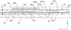
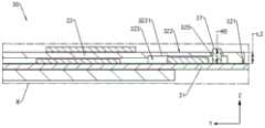
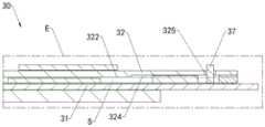
电路板组件30包括第一电路板31、第二电路板32、第一电子元器件34及第二电子元器件33。The
其中,第二电路板32具有相背设置的第一板面321及第二板面322。第一板面321连接于第一电路板31。可以理解的是,连接包括可拆卸连接以及不可拆卸连接。第二板面322背离第一电路板31设置。一种实施方式中,第二电路板32的第一板面321通过焊接工艺固定连接于第一电路板31。在其他实施方式中,第二电路板32的第一板面321也可以通过粘胶固定连接于第一电路板31。The
请参阅附图5,图5是图3所示的电路板组件在A-A线的一种实施方式的剖面示意图。Please refer to FIG. 5 . FIG. 5 is a schematic cross-sectional view of an embodiment of the circuit board assembly shown in FIG. 3 at line A-A.
第二电路板32设有第一凹槽324及第二凹槽323。第一凹槽324的开口位于第一板面321,也即第一凹槽324自第一板面321向第二电路板32的内部的方向凹陷。一种实施方式中,第一凹槽324在Y-Z平面的形状为矩形。在其他实施方式中,第一凹槽324在Y-Z平面的形状也可以为椭圆形。具体的本申请不做限定。The
第二凹槽323的开口位于第一板面321,也即第二凹槽323自第一板面321向第二电路板32的内部的方向凹陷。一种实施方式中,第二凹槽323在Y-Z平面的形状为矩形。在其他实施方式中,第二凹槽323在Y-Z平面的形状也可以为椭圆形。具体的本申请不做限定。The opening of the
此外,第二凹槽323连通至第一凹槽324,也即第二凹槽323与第一凹槽324形成一个整体的凹槽。附图5通过虚线将第一凹槽324与第二凹槽323分开。在其他实施方式中,第二凹槽323也可以未连通至第一凹槽324。In addition, the
请参阅图6,图6是图5所示的电路板组件在B处的一种实施方式的放大示意图。Please refer to FIG. 6 , which is an enlarged schematic view of an embodiment of the circuit board assembly at B shown in FIG. 5 .
第二凹槽323的底壁3231与第一凹槽324的底壁3241呈阶梯状。The
第一凹槽324在第一方向的深度d2小于第二凹槽323在第一方向的深度d1。第一方向为垂直于第二电路板33的板面的方向,也即第一方向为Z方向。可以理解的是,第一凹槽324在Z方向上的深度d2指的是第一凹槽324的底壁3241与第一板面321之间的距离。第二凹槽323在Z方向上的深度d1指的是第二凹槽323的底壁3231与第一板面321之间的距离。The depth d2 of the
此外,第一电子元器件34与第二电子元器件33均固定于第一电路板31。一种实施方式中,第一电子元器件34通过焊接工艺固定连接于第一电路板31。在其他实施方式中,第一电子元器件34也可以通过导电胶固定连接于第一电路板31。In addition, the first
第一电子元器件34位于第一凹槽324内。可以理解的是,第一电子元器件34可以部分位于第一凹槽324内,也可以全部位于第一凹槽324内。此时,第一电子元器件34与第二电路板32在Z方向具有重叠区域。The first
一种实施方式中,第一电子元器件34可以为但不仅限于为电源管理单元(powermanagement unit,PMU)。在其他实施方式中,第一电子元器件34也可以为外置设备驱动芯片,例如闪光灯驱动芯片。In one embodiment, the first
第二电子元器件33位于第二凹槽323内。可以理解的是,第二电子元器件33可以部分位于第二凹槽323内,也可以全部位于第二凹槽323内。此时,第二电子元器件33与第二电路板32在Z方向具有重叠区域。The second
一种实施方式中,第二电子元器件33可以为但不仅限于为电容。电容可以通过第一电路板31电连接于PMU。在其他实施方式中,第二电子元器件33也可以为电阻。In one embodiment, the second
此外,第一电子元器件34在Z方向的高度H2小于第二电子元器件33在Z方向的高度H1。可以理解的是,第一电子元器件34包括相背设置的第一端面341与第二端面342。第一端面341为第一电子元器件34靠近第一电路板31的端面。第二端面342为第一电子元器件34靠近第一凹槽324的底壁3241的端面。第一电子元器件34在Z方向的高度H2指的是第一端面341与第二端面342之间的距离。In addition, the height H2 of the first
此外,第二电子元器件33包括相背设置的第三端面331与第四端面332。第三端面331为第二电子元器件33靠近第一电路板31的端面。第四端面332为第二电子元器件33靠近第二凹槽323的底壁3231的端面。第二电子元器件33在Z方向的高度H1指的是第三端面331与第四端面332之间的距离。In addition, the second
可以理解的是,相较于在第二电路板32上开设一个凹槽,并将第一电子元器件34与第二电子元器件33共同位于该凹槽内,本实施方式通过将高度较低的第一电子元器件34位于深度较浅的第一凹槽324内,将高度较高的第二电子元器件33位于深度较深的第二凹槽323,从而既可以避免第二电路板32因开设的凹槽较大而降低第二电路板32的整体强度,又可以使得第一凹槽324的空间与第二凹槽323的空间能够得到有效地利用,也即显著提高第一凹槽324与第二凹槽323的空间利用率。It can be understood that, compared to opening a groove on the
在本实施方式中,通过在第二电路板32设置第一凹槽324与第二凹槽323,并使第一电子元器件34位于第一凹槽324内,第二电子元器件33位于第二凹槽323内,从而使得第一电子元器件34在Z方向上能够与第二电路板32具有重叠区域,第二电子元器件33在Z方向上能够与第二电路板32具有重叠区域,进而使得电路板组件30在Z方向上的厚度显著地减小。此时,电子设备100在Z方向上的厚度也能够显著地降低,也即电子设备100能够实现薄型化设置。In this embodiment, by disposing the
此外,当第一电子元器件34位于第一凹槽324内,第二电子元器件33位于第二凹槽323内时,第一凹槽324的槽壁可用于保护第一电子元器件34。第二凹槽323的槽壁可用于保护第二电子元器件33。In addition, when the first
此外,通过将第二电路板32层叠于第一电路板31,从而避免第二电路板32与第一电路板31因平铺于收容空间11内而增大电路板在X-Y平面的面积。故而,本申请的电路板组件30在X-Y平面的面积较小。In addition, by stacking the
可以理解的是,通过将第二凹槽323连通至第一凹槽324,以使第一凹槽324与第二凹槽323形成一个较大的凹槽,此时,在将第二电路板32连接于第一电路板31时,第一电子元器件34可以准确位于第一凹槽324,第二电子元器件33可以准确位于第二凹槽323内,也即电路板组件30的装配过程较简单。换言之,当第一凹槽324与第二凹槽323未连通时,第一凹槽324与第二凹槽323之间具有隔板。此时,在将第二电路板32连接于第一电路板31时,隔板将会影响第一电子元器件34位于第一凹槽324,第二电子元器件33位于第二凹槽323内,也即隔板将增加第二电路板32连接于第一电路板31的困难度。It can be understood that, by connecting the
请再次参阅图6,第一电子元器件34的第二端面342与第一凹槽324的底壁3241之间的距离小于或等于0.1毫米。此时,第一电子元器件34与第二电路板32之间具有一定的缓冲空间。当第二电路板32发生较小的变形时,第二电路板32不容易挤压到第一电子元器件34。Referring to FIG. 6 again, the distance between the
此外,第二电子元器件33的第四端面332与第二凹槽323的底壁3231之间的距离小于或等于0.1毫米。此时,第二电子元器件33与第二电路板32之间也具有一定的缓冲空间。当第二电路板32发生较小的变形时,第二电路板32不容易挤压到第二电子元器件33。In addition, the distance between the
请再次参阅图5,并结合图4所示,电路板组件30还包括第六电子元器件50。第六电子元器件50可以为但不仅限于为中央处理器(central processing unit,CPU)。第六电子元器件50固定连接于第一电路板31背离第二电路板32的表面。一种实施方式中,第六电子元器件50通过焊接工艺固定连接于第一电路板31背离第二电路板32的表面。在其他实施方式中,第六电子元器件50也可以通过导电胶固定连接于第一电路板31背离第二电路板32的表面。Please refer to FIG. 5 again, and in conjunction with FIG. 4 , the
一种实施方式中,CPU可通过第一电路板31电连接于屏幕20。此时,CPU可用于控制屏幕20内的应用软件的启动。具体的,当用户触碰屏幕20上的一个应用软件时,屏幕20能够产生触控信号,并将触控信号传递给CPU。CPU接收触控信号之后,根据触控信号启动应用软件。In one embodiment, the CPU can be electrically connected to the
请再次参阅图5,并结合图4所示,电路板组件30还包括第三电子元器件35。第三电子元器件35固定连接于第二板面322。此时,第三电子元器件35与第一电子元器件34及第二电子元器件33的类型不同。例如,第三电子元器件35为射频收发芯片。射频收发芯片通过第二电路板32电连接于天线的辐射体。此时,射频收发芯片能够向天线的辐射体发射射频信号。射频信号经第二电路板32耦合馈电至辐射体。辐射体根据射频信号辐射天线信号。此外,辐射体也能够接收电子设备100外部的天线信号,并将天线信号转换为射频信号,并将射频信号传输给射频收发电路。Please refer to FIG. 5 again, and in conjunction with FIG. 4 , the
可以理解的是,当在第二板面322固定连接第三电子元器件35时,电路板组件30上的电子元器件的数量将显著地增加,也即电路板组件30集成的电子元器件的数量较多。此时,电路板组件30的集成程度较高。换言之,电子设备100的收容空间11不会因电子元器件散乱排布而导致收容空间11的部分空间无法使用,也即收容空间11的空间利用率较低。It can be understood that when the third
请再次参考图5,第二电路板32设有第三凹槽326。第三凹槽326的开口位于第一板面321,也即第三凹槽326自第一板面321向第二电路板32内部的方向凹陷。一种实施方式中,第三凹槽326在Y-Z平面的形状为矩形。在其他实施方式中,第三凹槽326在Y-Z平面的形状也可以为椭圆形。具体的本申请不做限定。Referring to FIG. 5 again, the
请参阅图7,并结合图6所示,图7是图5所示的电路板组件在C处的放大示意图。第三凹槽326在Z方向的深度d3大于第二凹槽323在Z方向的深度d1。可以理解的是,第三凹槽326在Z方向上的深度d3指的是第三凹槽326的底壁3261与第一板面321之间的距离。Please refer to FIG. 7 in conjunction with FIG. 6 . FIG. 7 is an enlarged schematic view of the circuit board assembly shown in FIG. 5 at C. FIG. The depth d3 of the
电路板组件30还包括第五电子元器件39。结合图4所示,第五电子元器件39位于第一电子元器件34背离第二电子元器件33的一侧。第五电子元器件39可以为但不仅限于为电感。The
第五电子元器件39固定连接于第一电路板31,且第五电子元器件39位于第三凹槽326内。可以理解的是,第五电子元器件39可以部分位于第三凹槽326内,也可以全部位于第三凹槽326内。一种实施方式中,第五电子元器件39通过焊接工艺固定连接于第一电路板31。在其他实施方式中,第五电子元器件39也可以通过导电胶固定连接于第一电路板31。The fifth
此外,第五电子元器件39在Z方向的高度H3大于第二电子元器件33在Z方向的高度H1。In addition, the height H3 of the fifth
在本实施方式中,通过在第二电路板32设置第三凹槽326,并将第五电子元器件39位于第三凹槽326内,从而使得第五电子元器件39在Z方向上能够与第二电路板32具有重叠区域,进而使得电路板组件30在Z方向上的厚度显著地减小。此时,电子设备100在Z方向上的厚度也能够显著地降低,也即电子设备100能够实现薄型化设置。In this embodiment, the
此外,当第五电子元器件39位于第三凹槽326内时,第三凹槽326的槽壁可用于保护第五电子元器件39。In addition, when the fifth
此外,通过将高度较高的第五电子元器件39单独位于深度较深的第三凹槽326,从而既可以降低第三凹槽326对第二电路板32在第一凹槽324与第二凹槽323处的强度的影响,又可以使得第三凹槽326的空间能够得到有效地利用,也即提高第三凹槽326的空间利用率。In addition, by placing the fifth
此外,当在第一电路板31固定连接第五电子元器件39时,电路板组件30的电子元器件的数量将进一步地显著增加,也即电路板组件30集成的电子元器件的数量进一步地增多。此时,电路板组件30的集成程度较高。换言之,电子设备100的收容空间11不会因电子元器件散乱排布而导致收容空间11的部分空间无法使用,也即收容空间11的空间利用率较低。In addition, when the fifth
在其他实施方式中,第二电路板32还可以设有第N凹槽,其中,N大于3。第N凹槽在Z方向上的深度大于第N-1凹槽326在Z方向上的深度。具体的,本申请不做限定。In other embodiments, the
请参阅图8a,图8a是图5所示的电路板组件在B处的另一种实施方式的放大示意图。第一电子元器件34包括多个子电子元器件。多个子电子元器件在Z方向的高度均不同。每两个子电子元器件的高度的差值均小于或等于0.1毫米。附图8a示意了第一电子元器件34包括第一子电子元器件341以及第二子电子元器件342。例如,第一子电子元器件341为电池管理芯片。第二子电子元器件342为基带电源管理芯片。Please refer to FIG. 8a , which is an enlarged schematic view of another embodiment of the circuit board assembly shown in FIG. 5 at B. As shown in FIG. The first
在本实施方式中,通过将多个子电子元器件共同位于第一凹槽324内,从而避免第二电路板32因开设较多的凹槽而降低第二电路板32的强度。此外,因为每两个子电子元器件的高度的差值均小于或等于0.1毫米,所以多个子电子元器件在Z方向的高度的差异较小。此时,当多个子电子元器件共同位于第一凹槽324内时,第一凹槽324内的空间能够得到较大程度地利用。In this embodiment, by co-locating a plurality of sub-electronic components in the
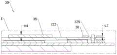
请参阅图8b,图8b是图5所示的电路板组件在B处的再一种实施方式的放大示意图。电路板组件30还包括第一补强板36。第一补强板36的材质可以为但不仅限于为钢片或者环氧玻璃布层压板。第一补强板36连接于第二板面322,且第一补强板36在第二板面322的投影与第二凹槽323的底壁3231在第二板面322的投影部分或全部重合。可以理解的是,连接包括可拆卸连接以及不可拆连接。Please refer to FIG. 8b , which is an enlarged schematic view of still another embodiment of the circuit board assembly shown in FIG. 5 at B. As shown in FIG. The
一种实施方式中,第一补强板36可以通过焊接固定连接于第二电路板32。在其他实施方式中,第一补强板36也可以通过粘胶固定连接于第二电路板32。具体的,本申请不做限制。In one embodiment, the first reinforcing
此外,第一补强板36在Z方向的高度L1小于或等于第三电子元器件35在Z方向的高度H4。可以理解的是,当第三电子元器件35的数量为多个时,第一补强板36在Z方向的高度L1小于或等于第三电子元器件35中高度最高的电子元器件。In addition, the height L1 of the first reinforcing
在本实施方式中,通过在第二板面322固定连接第一补强板36,且第一补强板36在第二板面322的投影与第二凹槽323的底壁3231在第二板面322的投影部分或全部重合,从而提高第二电路板32在第二凹槽323处的强度,进而避免第二电路板32在第二凹槽323处发生断裂。In this embodiment, the first reinforcing
此外,通过将第一补强板36在Z方向的高度L1小于或等于第三电子元器件35在Z方向的高度H4,从而保证电路板组件30整体强度提高的同时,电路板组件30在Z方向上的厚度也不会因在第二板面322设置第一补强板36而显著增加。In addition, by making the height L1 of the first reinforcing
请参阅图9,图9是图5所示的电路板组件在B处的再一种实施方式的放大示意图。第二电路板32设有通孔325。通孔325自第二凹槽323的底壁3231贯穿至第二板面322。一种实施方式中,通孔325可以为但不限于为圆柱孔。例如,通孔325也可以为异形孔。Please refer to FIG. 9 . FIG. 9 is an enlarged schematic view of still another embodiment of the circuit board assembly shown in FIG. 5 at B. FIG. The
电路板组件30还包括第四电子元器件37。第四电器元器件37在Z方向的高度H5小于第二电路板32在Z方向的高度L2。第二电路板32在Z方向的高度L2为第一板面321及第二板面322之间的距离。此时,第四电子元器件37固定连接于第一电路板31,且部分第四电子元器件37经第一凹槽324与通孔325穿出第二电路板32。第四电子元器件37可以为但不仅限于为功率电感。The
可以理解的是,当在第一电路板31固定连接有第四电子元器件37时,电路板组件30的电子元器件的数量将进一步地显著增加,也即电路板组件30集成的电子元器件的数量进一步地增多。此时,电路板组件30的集成程度较高。换言之,电子设备100的收容空间11不会因电子元器件散乱排布而导致收容空间11的部分空间无法使用,也即收容空间11的空间利用率较低。It can be understood that when the fourth
此外,通过在第二电路板32设置通孔325,以使高度较高的第四电子元器件37部分经第一凹槽324与通孔325穿出第二电路板32,从而使得第四电子元器件37在Z方向上与第二电路板32的重叠区域较大化,进而使得电路板组件30在Z方向上的厚度将显著地减小。此时,电子设备100在Z方向上的厚度也能够显著地降低,也即电子设备100能够实现薄型化设置。In addition, by disposing the through
请参阅图10a,图10a是图5所示的电路板组件在B处的再一种实施方式的放大示意图。电路板组件30还包括第二补强板38。第二补强板38的材质可以为但不仅限于为钢片或者环氧玻璃布层压板。第二补强板38固定连接于第二板面322,且环绕通孔325设置。第二补强板38的形状可以为但不仅限于为环状。例如第二补强板38的形状也可以为框状。一种实施方式中,第二补强板38可以通过焊接固定连接于第二电路板32。在其他实施方式中,第二补强板38也可以通过粘胶固定连接于第二电路板32。具体的,本申请不做限制。Please refer to FIG. 10a. FIG. 10a is an enlarged schematic view of still another embodiment of the circuit board assembly shown in FIG. 5 at B. FIG. The
此外,第二补强板38在Z方向的高度L3小于或等于第三电子元器件35在Z方向的高度H4。可以理解的是,当第三电子元器件35的数量为多个时,第二补强板38在Z方向的高度L3小于或等于第三电子元器件35中高度最高的电子元器件。In addition, the height L3 of the second reinforcing
在本实施方式中,当第二补强板38固定连接于第二板面322,且环绕通孔325设置时,第二补强板38能够提高通孔325周边处的强度,从而避免第二电路板32在通孔325处发生断裂。In this embodiment, when the second reinforcing
此外,通过设置第二补强板38在Z方向的高度L3小于或等于第三电子元器件35在Z方向的高度H4,从而保证电路板组件30整体强度提高的同时,电路板组件30在Z方向上的厚度也不会因在第二板面322设置第二补强板38而显著增加。In addition, by setting the height L3 of the second reinforcing
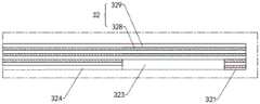
请参阅图10b,图10b是图5所示的电路板组件的第二电路板的另一种实施方式的部分剖面示意图。第二电路板32包括堆叠设置的多层导电层328和多层绝缘层329。相邻两层导电层328之间设有一层绝缘层329。第一凹槽324贯穿m层导电层328。第二凹槽323贯穿n层导电层328。其中,m小于n。Please refer to FIG. 10b, which is a partial cross-sectional schematic diagram of another embodiment of the second circuit board of the circuit board assembly shown in FIG. 5. FIG. The
在本实施方式中,m等于1。n等于2。此时,通过自第一板面321向第二电路板32内部去除一层绝缘层329与一层导电层328,以形成第一凹槽324。此外,通过自第一板面321向第二电路板32内部去除两层绝缘层329与两层导电层328,以形成第二凹槽323。在其他实施方式中,m也可以为其他数值。n也可以为其他数值。此时,通过去除相应数量的导电层328以及绝缘层329,以形成不同深度的凹槽。In this embodiment, m is equal to 1. n is equal to 2. At this time, a
可以理解的是,通过贯穿不同层数的导电层328,以获得不同深度的第一凹槽323以及第二凹槽324。该方式所获得的第一凹槽323与第二凹槽324的深度的准确度较高,且容易加工。It can be understood that the
上文具体介绍了电路板组件的第一种设置方式,第一种实施方式中的电路板组件30在保证Z方向的厚度较薄的同时,电路板组件30的整体强度也较佳。下文将结合相关附图具体介绍电路板组件30的第二种设置方式。The first configuration mode of the circuit board assembly is described above in detail. The
第二种实施方式,与第一种实施方式相同的内容不再赘述:请参阅图11及图12,图11是图1所示电子设备的电路板组件的另一种实施方式的结构示意图。图12是图11所示的电路板组件的部分分解示意图。In the second embodiment, the same content as the first embodiment will not be repeated: please refer to FIG. 11 and FIG. 12 . FIG. 11 is a schematic structural diagram of another embodiment of the circuit board assembly of the electronic device shown in FIG. 1 . FIG. 12 is a partially exploded schematic view of the circuit board assembly shown in FIG. 11 .
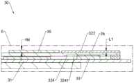
电路板组件30包括第一电路板31、架高板40、第二电路板32、第一电子元器件34以及第二电子元器件33。The
其中,架高板40呈中空结构,也即架高板40围成一镂空区域。一种实施方式中,架高板40的形状可以为但不仅限于为框状。例如,架高板40的形状也可以为环状结构。The
此外,架高板40连接于第一电路板31的板面。可以理解的是,连接包括可拆卸连接以及不可拆连接。一种实施方式中,架高板40可以通过焊接固定连接于第一电路板31的板面。在其他实施方式中,架高板40也可以通过粘胶固定连接于第一电路板31。具体的,本申请不做限制。In addition, the
此外,第二电路板32包括相背设置的第一板面321及第二板面322。第二电路板32的部分第一板面321连接于架高板40远离第一电路板31的一侧。一种实施方式中,第二电路板32可以通过焊接固定于架高板40远离第一电路板31的一侧。在其他实施方式中,第二电路板32也可以通过粘胶固定于架高板40远离第一电路板31的一侧。具体的,本申请不做限制。In addition, the
请参阅图13及图14,图13是图11所示电路板组件在D-D线处的剖面示意图。图14是图13所示的电路板组件在E处的放大示意图。Please refer to FIGS. 13 and 14. FIG. 13 is a schematic cross-sectional view of the circuit board assembly shown in FIG. 11 at the line D-D. FIG. 14 is an enlarged schematic view at E of the circuit board assembly shown in FIG. 13 .
第二电路板32、架高板40及第一电路板31共同围设出收纳空间S。The
第二电路板32设有第一凹槽324。第一凹槽324的开口位于第一板面321,也即第一凹槽324自第一板面321向第二电路板32的内部凹陷。第一凹槽324连通收纳空间S。此时,第一凹槽324与部分收纳空间S所形成的空间在Z方向上的深度较深。The
此外,第一电子元器件34及第二电子元器件33均固定于第一电路板31。In addition, the first
第一电子元器件34在Z方向上的高度H2小于第二电子元器件33在Z方向上的高度H1。可以理解的是,第一电子元器件34包括相背设置的第一端面341与第二端面342。第一端面341为第一电子元器件34靠近第一电路板31的端面。第二端面342为第一电子元器件34靠近第二电路板32的端面。第一电子元器件34在Z方向的高度H2指的是第一端面341与第二端面342之间的距离。此外,第二电子元器件33包括相背设置的第三端面331与第四端面332。第三端面331为第二电子元器件33靠近第一电路板31的端面。第四端面332为第二电子元器件33靠近第一凹槽324的底壁3241的端面。第二电子元器件33在Z方向的高度H1指的是第三端面331与第四端面332之间的距离。The height H2 of the first
第一电子元器件34位于收纳空间S。第二电子元器件33部分位于收纳空间S、部分位于第一凹槽324内。The first
在本实施方式中,通过在第二电路板32开设第一凹槽324,并将高度较高的第二电子元器件33部分位于第一凹槽324内,部分设于收纳空间S内,从而在Z方向上第二电子元器件33与第二电路板32具有重叠区域,进而显著地降低电路板组件30在Z方向上的厚度。In this embodiment, a
此外,当第二电子元器件33部分位于收纳空间S、部分位于第一凹槽324内时,第一凹槽324的槽壁以及架高板40也可用于保护第二电子元器件33。In addition, when the second
此外,通过将高度较低的第二电子元器件33位于收纳空间S内,从而既可以通过架高板40保护第一电子元器件34,又可以有效地利用收纳空间S,以提高收纳空间S的空间利用率。In addition, by locating the second
此外,通过在第一电路板31依次连接架高板40和第二电路板32,从而避免第一电路板31与第二电路板32因平铺于收容空间11内而占用收容空间11内的体积。故而,本申请的电路板组件30在X-Y平面的面积较小。In addition, by sequentially connecting the
一种实施方式中,第一电子元器件34的第二端面342与第一板面321之间的距离小于或等于0.1毫米。此时,第一电子元器件34与第一板面321之间也具有一定的缓冲空间。当第二电路板32发生较小的变形时,第二电路板32不容易挤压到第一电子元器件34。In one embodiment, the distance between the
此外,第二电子元器件33的第四端面332与第一凹槽324的底壁3241之间的距离小于或等于0.1毫米。此时,第二电子元器件33与第一凹槽324的底壁3241之间具有一定的缓冲空间。当第二电路板32发生较小的变形时,第二电路板32不容易挤压到第二电子元器件33。In addition, the distance between the
请再次参阅图13,并结合图12,电路板组件30还包括第三电子元器件35。第三电子元器件35固定连接于第二板面322。第三电子元器件35与第一电子元器件34及第二电子元器件33的类型不同。具体的,本实施方式的第三电子元器件35的类型以及固定方式可参考第一种实施方式的第三电子元器件35的类型和固定方式。这里不再赘述。Please refer to FIG. 13 again, and in conjunction with FIG. 12 , the
请参阅图15,并结合附图14所示,图15是图13所示的电路板组件在G处的一种实施方式的放大示意图。第二电路板32设有第二凹槽323。第二凹槽323连通收纳空间S。第二凹槽323在Z方向的深度大于第一凹槽324在Z方向的深度。Please refer to FIG. 15 in conjunction with FIG. 14 . FIG. 15 is an enlarged schematic view of an embodiment of the circuit board assembly shown in FIG. 13 at G. The
电路板组件30还包括第五电子元器件39。第五电子元器件39固定连接于第一电路板31,且第五电子元器件39部分位于收纳空间S,部分位于第二凹槽323。第五电子元器件39在Z方向的高度H3大于第二电子元器件33在Z方向的高度H1。The
在本实施方式中,通过在第二电路板32设置第二凹槽323,并将第五电子元器件39部分设于收纳空间S,部分位于第二凹槽323内,从而使得第五电子元器件39在Z方向上能够与第二电路板32具有重叠区域,进而使得电路板组件30在Z方向上的厚度显著地减小。此时,电子设备100在Z方向上的厚度也能够显著地降低,也即电子设备100能够实现薄型化设置。In this embodiment, the
此外,当第五电子元器件39位于第二凹槽323内时,第二凹槽323的槽壁可用于保护第五电子元器件39。In addition, when the fifth
请参阅图16,图16是图13所示的电路板组件在E处的另一种实施方式的放大示意图。电路板组件30还包括第一补强板36。第一补强板36固定连接于第二板面322。第一补强板36在第二板面322的投影与第一凹槽324的底壁3241在第二板面322的投影部分或者全部重叠。第一补强板36在Z方向上的高度L1小于或等于第三电子元器件35的高度H4。具体的,第一补强板36的材料及固定方式可参考第一种实施方式的第一补强板36的材料及固定方式。这里不再赘述。Please refer to FIG. 16, which is an enlarged schematic view of another embodiment of the circuit board assembly shown in FIG. 13 at E. The
请参阅图17,图17是图13所示的电路板组件在E处的再一种实施方式的放大示意图。电路板组件30还包括第四电子元器件37。第二电路板32设有通孔325。通孔325自第一凹槽324的底壁3241贯穿至第二板面322。第四电子元器件37固定连接于第一电路板31。部分第四电子元器件37位于收纳空间S,部分位于第一凹槽324内,部分位于通孔325内。具体的,第四电子元器件37固定方式可参考第一种实施方式的第四电子元器件37的固定方式。这里不再赘述。Please refer to FIG. 17 . FIG. 17 is an enlarged schematic view of still another embodiment of the circuit board assembly at E shown in FIG. 13 . The
请参阅图18,图18是图13所示的电路板组件在E处的再一种实施方式的放大示意图。电路板组件30还包括第二补强板38。第二补强板38固定连接于第二板面322,且环绕通孔325设置。第二补强板38在Z方向的高度L2小于或等于第三电子元器件35在Z方向的高度H4。具体的,第二补强板38的材料及设置方式可参考第一种实施方式的第二补强板38的材料及设置方式。这里不再赘述。Please refer to FIG. 18 , FIG. 18 is an enlarged schematic view of still another embodiment of the circuit board assembly at E shown in FIG. 13 . The
上文具体描述了电路板组件30的第二种设置方式。在本实施方式中,电路板组件30在Z方向上的厚度较薄。此时,电路板组件30应用于电子设备100时,电子设备100在Z方向上的厚度较薄,也即电子设备100能够实现薄型化设置。The second arrangement of the
以上,仅为本申请的具体实施方式,但本申请的保护范围并不局限于此,任何熟悉本技术领域的技术人员在本申请揭露的技术范围内,可轻易想到变化或替换,都应涵盖在本申请的保护范围之内。因此,本申请的保护范围应以权利要求的保护范围为准。The above are only specific embodiments of the present application, but the protection scope of the present application is not limited to this. Any person skilled in the art who is familiar with the technical scope disclosed in the present application can easily think of changes or replacements, which should cover within the scope of protection of this application. Therefore, the protection scope of the present application shall be subject to the protection scope of the claims.
Claims (19)
Priority Applications (1)
| Application Number | Priority Date | Filing Date | Title |
|---|---|---|---|
| CN201922120143.7UCN211481600U (en) | 2019-11-30 | 2019-11-30 | Circuit board assembly and electronic equipment |
Applications Claiming Priority (1)
| Application Number | Priority Date | Filing Date | Title |
|---|---|---|---|
| CN201922120143.7UCN211481600U (en) | 2019-11-30 | 2019-11-30 | Circuit board assembly and electronic equipment |
Publications (1)
| Publication Number | Publication Date |
|---|---|
| CN211481600Utrue CN211481600U (en) | 2020-09-11 |
Family
ID=72362963
Family Applications (1)
| Application Number | Title | Priority Date | Filing Date |
|---|---|---|---|
| CN201922120143.7UActiveCN211481600U (en) | 2019-11-30 | 2019-11-30 | Circuit board assembly and electronic equipment |
Country Status (1)
| Country | Link |
|---|---|
| CN (1) | CN211481600U (en) |
Cited By (3)
| Publication number | Priority date | Publication date | Assignee | Title |
|---|---|---|---|---|
| CN113891556A (en)* | 2021-10-13 | 2022-01-04 | Oppo广东移动通信有限公司 | Electronic equipment and circuit board assembly thereof |
| CN114697792A (en)* | 2020-12-31 | 2022-07-01 | 华为技术有限公司 | a headphone |
| WO2024093243A1 (en)* | 2022-10-31 | 2024-05-10 | 荣耀终端有限公司 | Electronic assembly and terminal device |
- 2019
- 2019-11-30CNCN201922120143.7Upatent/CN211481600U/enactiveActive
Cited By (3)
| Publication number | Priority date | Publication date | Assignee | Title |
|---|---|---|---|---|
| CN114697792A (en)* | 2020-12-31 | 2022-07-01 | 华为技术有限公司 | a headphone |
| CN113891556A (en)* | 2021-10-13 | 2022-01-04 | Oppo广东移动通信有限公司 | Electronic equipment and circuit board assembly thereof |
| WO2024093243A1 (en)* | 2022-10-31 | 2024-05-10 | 荣耀终端有限公司 | Electronic assembly and terminal device |
Similar Documents
| Publication | Publication Date | Title |
|---|---|---|
| US11056771B2 (en) | Antenna module and electronic device | |
| CN211481600U (en) | Circuit board assembly and electronic equipment | |
| CN108270071B (en) | Antenna module, middle frame module and electronic equipment | |
| US9743564B2 (en) | Electromagnetic shielding structures | |
| CN207541546U (en) | Display screen and electronic equipment | |
| CN103885631B (en) | touch display device with flexible circuit module | |
| CN108258425A (en) | Antenna module, middle frame module and electronic equipment | |
| CN105072221B (en) | Display screen assembling structure and its mobile terminal device | |
| WO2019052332A1 (en) | Display screen assembly and mobile terminal | |
| CN110023877B (en) | Assembling method and terminal | |
| CN108539369B (en) | Antenna assembly, manufacturing method of antenna assembly and electronic equipment | |
| EP4044783A1 (en) | Shielding apparatus and electronic device | |
| CN117652135A (en) | Electronic device comprising a protective cover for protecting a flexible display | |
| KR20230045368A (en) | Electronic components assembly and electronic device thereof | |
| CN207853955U (en) | Displays and Electronics | |
| CN111867238A (en) | Printed circuit board assemblies and electronic equipment | |
| CN209150118U (en) | Flexible display structure and electronic equipment | |
| CN214846481U (en) | Display module and electronic equipment | |
| CN112995373B (en) | Display components and electronics | |
| CN110502071A (en) | Screen components and terminal equipment | |
| CN108539370A (en) | Shell assembly, antenna assembly, electronic equipment and machining method | |
| WO2021093624A1 (en) | Terminal having stiffener | |
| WO2022134026A1 (en) | Flexible circuit board and display apparatus | |
| CN108539373B (en) | Housing assembly, antenna assembly, manufacturing method of antenna assembly, and electronic device | |
| CN205584486U (en) | Speaker assembly and mobile terminal |
Legal Events
| Date | Code | Title | Description |
|---|---|---|---|
| GR01 | Patent grant | ||
| GR01 | Patent grant | ||
| TR01 | Transfer of patent right | Effective date of registration:20210506 Address after:Unit 3401, unit a, building 6, Shenye Zhongcheng, No. 8089, Hongli West Road, Donghai community, Xiangmihu street, Futian District, Shenzhen, Guangdong 518040 Patentee after:Honor Device Co.,Ltd. Address before:518129 Bantian HUAWEI headquarters office building, Longgang District, Guangdong, Shenzhen Patentee before:HUAWEI TECHNOLOGIES Co.,Ltd. | |
| TR01 | Transfer of patent right | ||
| CP03 | Change of name, title or address | Address after:Unit 3401, unit a, building 6, Shenye Zhongcheng, No. 8089, Hongli West Road, Donghai community, Xiangmihu street, Futian District, Shenzhen, Guangdong 518040 Patentee after:Honor Terminal Co.,Ltd. Country or region after:China Address before:3401, unit a, building 6, Shenye Zhongcheng, No. 8089, Hongli West Road, Donghai community, Xiangmihu street, Futian District, Shenzhen, Guangdong Patentee before:Honor Device Co.,Ltd. Country or region before:China | |
| CP03 | Change of name, title or address |