CN211295694U - Laser drivers and LiDAR devices - Google Patents
Laser drivers and LiDAR devicesDownload PDFInfo
- Publication number
- CN211295694U CN211295694UCN201890000589.7UCN201890000589UCN211295694UCN 211295694 UCN211295694 UCN 211295694UCN 201890000589 UCN201890000589 UCN 201890000589UCN 211295694 UCN211295694 UCN 211295694U
- Authority
- CN
- China
- Prior art keywords
- laser
- laser driver
- inductor
- switch
- transistor
- Prior art date
- Legal status (The legal status is an assumption and is not a legal conclusion. Google has not performed a legal analysis and makes no representation as to the accuracy of the status listed.)
- Active
Links
Images


Classifications
- H—ELECTRICITY
- H01—ELECTRIC ELEMENTS
- H01S—DEVICES USING THE PROCESS OF LIGHT AMPLIFICATION BY STIMULATED EMISSION OF RADIATION [LASER] TO AMPLIFY OR GENERATE LIGHT; DEVICES USING STIMULATED EMISSION OF ELECTROMAGNETIC RADIATION IN WAVE RANGES OTHER THAN OPTICAL
- H01S5/00—Semiconductor lasers
- H01S5/04—Processes or apparatus for excitation, e.g. pumping, e.g. by electron beams
- H01S5/042—Electrical excitation ; Circuits therefor
- H01S5/0428—Electrical excitation ; Circuits therefor for applying pulses to the laser
- G—PHYSICS
- G01—MEASURING; TESTING
- G01S—RADIO DIRECTION-FINDING; RADIO NAVIGATION; DETERMINING DISTANCE OR VELOCITY BY USE OF RADIO WAVES; LOCATING OR PRESENCE-DETECTING BY USE OF THE REFLECTION OR RERADIATION OF RADIO WAVES; ANALOGOUS ARRANGEMENTS USING OTHER WAVES
- G01S7/00—Details of systems according to groups G01S13/00, G01S15/00, G01S17/00
- G01S7/48—Details of systems according to groups G01S13/00, G01S15/00, G01S17/00 of systems according to group G01S17/00
- G01S7/481—Constructional features, e.g. arrangements of optical elements
- G01S7/4814—Constructional features, e.g. arrangements of optical elements of transmitters alone
- G—PHYSICS
- G01—MEASURING; TESTING
- G01S—RADIO DIRECTION-FINDING; RADIO NAVIGATION; DETERMINING DISTANCE OR VELOCITY BY USE OF RADIO WAVES; LOCATING OR PRESENCE-DETECTING BY USE OF THE REFLECTION OR RERADIATION OF RADIO WAVES; ANALOGOUS ARRANGEMENTS USING OTHER WAVES
- G01S7/00—Details of systems according to groups G01S13/00, G01S15/00, G01S17/00
- G01S7/48—Details of systems according to groups G01S13/00, G01S15/00, G01S17/00 of systems according to group G01S17/00
- G01S7/481—Constructional features, e.g. arrangements of optical elements
- G01S7/4816—Constructional features, e.g. arrangements of optical elements of receivers alone
- G—PHYSICS
- G01—MEASURING; TESTING
- G01S—RADIO DIRECTION-FINDING; RADIO NAVIGATION; DETERMINING DISTANCE OR VELOCITY BY USE OF RADIO WAVES; LOCATING OR PRESENCE-DETECTING BY USE OF THE REFLECTION OR RERADIATION OF RADIO WAVES; ANALOGOUS ARRANGEMENTS USING OTHER WAVES
- G01S7/00—Details of systems according to groups G01S13/00, G01S15/00, G01S17/00
- G01S7/48—Details of systems according to groups G01S13/00, G01S15/00, G01S17/00 of systems according to group G01S17/00
- G01S7/483—Details of pulse systems
- G01S7/484—Transmitters
- H—ELECTRICITY
- H01—ELECTRIC ELEMENTS
- H01S—DEVICES USING THE PROCESS OF LIGHT AMPLIFICATION BY STIMULATED EMISSION OF RADIATION [LASER] TO AMPLIFY OR GENERATE LIGHT; DEVICES USING STIMULATED EMISSION OF ELECTROMAGNETIC RADIATION IN WAVE RANGES OTHER THAN OPTICAL
- H01S5/00—Semiconductor lasers
- H01S5/06—Arrangements for controlling the laser output parameters, e.g. by operating on the active medium
- H01S5/068—Stabilisation of laser output parameters
- H01S5/06825—Protecting the laser, e.g. during switch-on/off, detection of malfunctioning or degradation
- H—ELECTRICITY
- H01—ELECTRIC ELEMENTS
- H01S—DEVICES USING THE PROCESS OF LIGHT AMPLIFICATION BY STIMULATED EMISSION OF RADIATION [LASER] TO AMPLIFY OR GENERATE LIGHT; DEVICES USING STIMULATED EMISSION OF ELECTROMAGNETIC RADIATION IN WAVE RANGES OTHER THAN OPTICAL
- H01S5/00—Semiconductor lasers
- H01S5/06—Arrangements for controlling the laser output parameters, e.g. by operating on the active medium
- H01S5/062—Arrangements for controlling the laser output parameters, e.g. by operating on the active medium by varying the potential of the electrodes
- H01S5/06209—Arrangements for controlling the laser output parameters, e.g. by operating on the active medium by varying the potential of the electrodes in single-section lasers
- H01S5/06216—Pulse modulation or generation
- H—ELECTRICITY
- H03—ELECTRONIC CIRCUITRY
- H03K—PULSE TECHNIQUE
- H03K5/00—Manipulating of pulses not covered by one of the other main groups of this subclass
- H03K5/01—Shaping pulses
- H03K5/04—Shaping pulses by increasing duration; by decreasing duration
Landscapes
- Physics & Mathematics (AREA)
- Engineering & Computer Science (AREA)
- General Physics & Mathematics (AREA)
- Computer Networks & Wireless Communication (AREA)
- Radar, Positioning & Navigation (AREA)
- Remote Sensing (AREA)
- Condensed Matter Physics & Semiconductors (AREA)
- Electromagnetism (AREA)
- Optics & Photonics (AREA)
- Optical Radar Systems And Details Thereof (AREA)
- Semiconductor Lasers (AREA)
Abstract
Description
Translated fromChinese技术领域technical field
本实用新型涉及一种激光驱动器以及LiDAR装置。具体地但非排他地说,本公开涉及用于LiDAR应用的短脉冲激光驱动器。The utility model relates to a laser driver and a LiDAR device. Specifically, but not exclusively, the present disclosure relates to short-pulse laser drivers for LiDAR applications.
背景技术Background technique
典型的现有技术ToF LiDAR系统使用脉冲或连续照明。后者使用可表示为正弦信号的连续时变信号。为了检测目标的范围,需要获取信号并确定输出与输入信号之间的任何相角偏移。接着使用该偏移来计算从源到目标的距离。Typical prior art ToF LiDAR systems use pulsed or continuous illumination. The latter uses a continuous time-varying signal that can be represented as a sinusoidal signal. In order to detect the range of the target, the signal needs to be acquired and any phase angle offset between the output and input signal needs to be determined. This offset is then used to calculate the distance from the source to the target.
用于脉冲照明的激光驱动器LiDAR应用以大于4ns的脉冲宽度为目标。此相对长的脉冲宽度限制可能由于眼睛安全问题而实现的峰值功率,并会增加范围不确定性。而且,迄今已知的激光驱动器消耗大量功率并需要高偏置电压。在一些现有技术驱动器中,所需的偏置电压超过200伏或更高。这是不合期望的。Laser driver LiDAR applications for pulsed illumination target pulse widths greater than 4 ns. This relatively long pulse width limits the peak power that can be achieved due to eye safety concerns and increases range uncertainty. Furthermore, hitherto known laser drivers consume a lot of power and require high bias voltages. In some prior art drivers, the required bias voltage exceeds 200 volts or more. This is not expected.
因此,需要一种解决现有技术的至少一些缺点的激光驱动器。Accordingly, there is a need for a laser driver that addresses at least some of the shortcomings of the prior art.
实用新型内容Utility model content
参考以下附图将更好地理解这些和其他特征,提供所述附图以有助于理解本教导。These and other features will be better understood with reference to the following drawings, which are provided to facilitate understanding of the present teachings.
因此,提供一种包括以下各项的激光驱动器:Accordingly, there is provided a laser driver comprising:
谐振电路,其具有电感器和DC阻隔电容器(DC blocking capacitor);a resonant circuit having an inductor and a DC blocking capacitor;
偏置电压基准(biasing voltage reference),其可操作地联接到所述电感器;以及a biasing voltage reference operably coupled to the inductor; and
控制器,其可操作地控制所述谐振电路,以在高阻抗和低阻抗之间选择性地连接所述电感器;其中所述DC阻隔电容器可操作地连接到激光二极管。a controller operable to control the resonant circuit to selectively connect the inductor between high impedance and low impedance; wherein the DC blocking capacitor is operably connected to the laser diode.
在一个方面中,当所述电感器连接到所述高阻抗时,所述电感器的至少一个端子连接到开路。In one aspect, when the inductor is connected to the high impedance, at least one terminal of the inductor is connected to an open circuit.
在另一方面中,当所述电感器连接到所述低阻抗时,至少一个端子被短接以接地。In another aspect, when the inductor is connected to the low impedance, at least one terminal is shorted to ground.
在另一方面中,所述控制器被配置为在高阻抗和低阻抗之间重复开关所述电感器。In another aspect, the controller is configured to repeatedly switch the inductor between high impedance and low impedance.
在示例性方面中,所述电感器具有在1nH到50nH的范围内的值。In an exemplary aspect, the inductor has a value in the range of 1 nH to 50 nH.
在另一方面中,所述DC阻隔电容器具有在10pF到1nF的范围内的值。In another aspect, the DC blocking capacitor has a value in the range of 10 pF to 1 nF.
在一个方面中,通过所述谐振电路产生感应激光驱动器电流。In one aspect, an induced laser driver current is generated through the resonant circuit.
在另一方面中,所述感应激光驱动器电流是脉冲信号。In another aspect, the inductive laser driver current is a pulsed signal.
在另一示例性方面中,所述脉冲信号的每个脉冲的宽度小于或等于1ns。In another exemplary aspect, the width of each pulse of the pulse signal is less than or equal to 1 ns.
在另一方面中,所述脉冲信号的每个脉冲的宽度在100ps到2ns的范围内。In another aspect, the width of each pulse of the pulsed signal is in the range of 100ps to 2ns.
在一个方面中,所述DC阻隔电容器可操作地连接到激光二极管的阳极。In one aspect, the DC blocking capacitor is operably connected to the anode of the laser diode.
在另一方面中,所述激光二极管的所述阴极可操作地联接成接地。In another aspect, the cathode of the laser diode is operably coupled to ground.
在另一方面中,所述DC阻隔电容器可操作地连接到激光二极管的阴极。In another aspect, the DC blocking capacitor is operably connected to the cathode of the laser diode.
在一个方面中,所述激光二极管的所述阳极可操作地联接成接地。In one aspect, the anode of the laser diode is operably coupled to ground.
在另一方面中,所述偏置电压基准可操作地提供正偏置电压。In another aspect, the bias voltage reference is operable to provide a positive bias voltage.
在一个方面中,所述正偏置电压在10V到50V的范围内。In one aspect, the forward bias voltage is in the range of 10V to 50V.
在另一方面中,所述偏置电压基准可操作地提供负偏置电压。In another aspect, the bias voltage reference is operable to provide a negative bias voltage.
在一个示例性方面中,所述控制器包括开关。In one exemplary aspect, the controller includes a switch.
在另一方面中,当所述开关闭合时,从所述电感器到接地提供路径,由此将所述电感器连接到低阻抗。In another aspect, when the switch is closed, a path is provided from the inductor to ground, thereby connecting the inductor to a low impedance.
在一个方面中,当所述开关断开时,所述电感器连接到高阻抗。In one aspect, the inductor is connected to high impedance when the switch is open.
在另一方面中,当所述开关断开时,到接地的路径与所述电感器隔离。In another aspect, when the switch is open, the path to ground is isolated from the inductor.
在一个方面中,提供可操作地来选择性地断开和闭合所述开关的控制电压参考。In one aspect, a control voltage reference operable to selectively open and close the switch is provided.
在另一方面中,所述控制电压参考可操作地提供脉冲电压参考。In another aspect, the control voltage reference is operable to provide a pulsed voltage reference.
在另一方面中,所述开关包括晶体管。In another aspect, the switch includes a transistor.
在另一方面中,所述偏置电压基准以在10V到50V的范围内的电压电平偏置所述电感器。In another aspect, the bias voltage reference biases the inductor at a voltage level in the range of 10V to 50V.
在一个方面中,跨越所述电感器产生感应EMF电压。In one aspect, an induced EMF voltage is generated across the inductor.
在另一方面中,所述感应EMF电压与所述偏置电压基准相反,直到达到稳态DC电压值。In another aspect, the induced EMF voltage is opposite to the bias voltage reference until a steady state DC voltage value is reached.
在另一方面中,所述控制器使所述开关在断开状态与闭合状态之间重复地循环。In another aspect, the controller repeatedly cycles the switch between an open state and a closed state.
在一个方面中,在所述循环中所述断开状态的时间段是≥10纳秒。In one aspect, the time period of the off state in the cycle is > 10 nanoseconds.
在另一方面中,在所述循环中所述闭合状态的时间段是10到100纳秒。In another aspect, the time period of the closed state in the cycle is 10 to 100 nanoseconds.
在另一方面中,所述断开状态与所述闭合状态的时间段基本上相等。In another aspect, the time periods of the open state and the closed state are substantially equal.
在另一方面中,所述控制器被配置为将脉冲驱动信号施加到所述开关以控制所述开关。In another aspect, the controller is configured to apply a pulsed drive signal to the switch to control the switch.
在一个方面中,当所述开关闭合时,流经所述电感器的DC电流无法突然停止,由此跨越所述电感器生成反EMF,且通过DC电流阻隔电容器C1和所述激光二极管转移由所述反EMF产生的感应电流。In one aspect, when the switch is closed, the DC current flowing through the inductor cannot abruptly stop, thereby generating a back EMF across the inductor and diverted by the DC current blocking capacitor C1 and the laser diode by the induced current generated by the back EMF.
在另一方面中,所述谐振电路以频率1/(2π(LC)1/2)谐振,该频率决定被注入到所述激光器中的所述感应电流脉冲的脉冲宽度。In another aspect, the resonant circuit resonates at a frequency of 1/(2π(LC)1/2 ) which determines the pulse width of the induced current pulse injected into the laser.
在示例性方面中,通过适当选择所述电感器和DC阻隔电容器值来调谐所述感应电流的所述脉冲宽度。In an exemplary aspect, the pulse width of the induced current is tuned by appropriate selection of the inductor and DC blocking capacitor values.
在另一方面中,提供保护二极管,所述保护二极管可操作地在所述谐振电路谐振时保护所述激光二极管以免受相反极性。In another aspect, a protection diode is provided that is operable to protect the laser diode from reverse polarity when the resonant circuit resonates.
在另一方面中,所述晶体管是氮化镓晶体管。In another aspect, the transistor is a gallium nitride transistor.
在一个方面中,所述控制器包括MOSFET驱动器。In one aspect, the controller includes a MOSFET driver.
在另一方面中,所述MOSFET驱动器可操作地以具有正和负分量的脉冲信号驱动所述氮化镓晶体管。In another aspect, the MOSFET driver is operable to drive the gallium nitride transistor with a pulsed signal having positive and negative components.
在另一方面中,所述脉冲信号的最大值对应于所述氮化镓晶体管的最大栅极源极电压范围。In another aspect, the maximum value of the pulse signal corresponds to a maximum gate-source voltage range of the gallium nitride transistor.
在一个方面中,所述脉冲信号在-6V到+6V的范围内。In one aspect, the pulsed signal is in the range of -6V to +6V.
在另一方面中,所述脉冲信号具有短工作周期。In another aspect, the pulsed signal has a short duty cycle.
在另一方面中,所述短工作周期在10Khz到200Mhz下是10ns到100ns。In another aspect, the short duty cycle is 10ns to 100ns at 10Khz to 200Mhz.
在一个方面中,当所述晶体管被驱动为耗尽而致使漏极源极电流突然关断时,所述晶体管的最大反向栅极源极电压(maximum reverse gate source voltage) 对应于栅极源极结值(Gate Source junction value)。In one aspect, the maximum reverse gate source voltage of the transistor corresponds to the gate source when the transistor is driven to depletion causing the drain source current to turn off abruptly Gate Source junction value.
在另一方面中,存储于所述电感器上的能量接着作为尖锐的电流脉冲通过所述DC阻隔电容器且被递送给所述激光二极管。In another aspect, the energy stored on the inductor is then delivered as a sharp current pulse through the DC blocking capacitor and to the laser diode.
本公开还涉及一种包括以下各项的LiDAR装置:The present disclosure also relates to a LiDAR device comprising:
激光驱动器,其包括:Laser driver, which includes:
谐振电路,其具有电感器和DC阻隔电容器;a resonant circuit with an inductor and a DC blocking capacitor;
偏置电压基准,其可操作地联接到所述电感器;以及a bias voltage reference operably coupled to the inductor; and
控制器,其可操作地控制所述谐振电路,以在高阻抗和低阻抗之间选择性地连接所述电感器;其中所述DC阻隔电容器可操作地连接到激光二极管;a controller operable to control the resonant circuit to selectively connect the inductor between high impedance and low impedance; wherein the DC blocking capacitor is operably connected to a laser diode;
激光器,其可操作地联接到所述激光驱动器;以及a laser operably coupled to the laser driver; and
光学检测器。Optical detector.
在一个方面中,光学检测器包括盖革模式检测器。In one aspect, the optical detector includes a Geiger mode detector.
在另一方面中,所述光学检测器包括SiPM检测器。In another aspect, the optical detector comprises a SiPM detector.
在另一方面中,所述光学检测器包括单个光子雪崩二极管(SPAD)。In another aspect, the optical detector includes a single photon avalanche diode (SPAD).
附图说明Description of drawings
现在将参考附图描述本教导,其中:The present teachings will now be described with reference to the accompanying drawings, wherein:
图1说明用于直接ToF测距(direct ToF ranging)的示例性技术。1 illustrates an exemplary technique for direct ToF ranging.
图2说明示例性ToF测距系统。2 illustrates an exemplary ToF ranging system.
图3说明使用图4的ToF测距系统生成的直方图。FIG. 3 illustrates a histogram generated using the ToF ranging system of FIG. 4 .
图4说明并入有SiPM检测器的示例性LiDAR设备。4 illustrates an exemplary LiDAR device incorporating a SiPM detector.
图5说明硅光电倍增管(SiPM)的示例性结构。5 illustrates an exemplary structure of a silicon photomultiplier (SiPM).
图6是示例性硅光电倍增器的示意性电路图。6 is a schematic circuit diagram of an exemplary silicon photomultiplier.
图7是根据本教导的激光驱动器的示意性电路图。7 is a schematic circuit diagram of a laser driver in accordance with the present teachings.
图8说明使用图7的激光驱动器的仿真信号图。FIG. 8 illustrates a simulated signal diagram using the laser driver of FIG. 7 .
图9是也根据本教导的另一激光驱动器的示意电路图。9 is a schematic circuit diagram of another laser driver also in accordance with the present teachings.
图10说明使用图9的激光驱动器产生的激光脉冲宽度图。FIG. 10 illustrates a graph of laser pulse widths produced using the laser driver of FIG. 9 .
图11说明也根据本教导的另一LiDAR设备。Figure 11 illustrates another LiDAR device also in accordance with the present teachings.
图12说明使用图11的LiDAR设备的激光脉冲宽度图。FIG. 12 illustrates a graph of laser pulse widths using the LiDAR device of FIG. 11 .
图13说明针对电感器L1的不同值而使用图11的LiDAR设备的激光脉冲宽度图。13 illustrates a graph of laser pulse widths using the LiDAR device of FIG. 11 for different values of inductor L1.
图14A和14B说明也根据本教导的另一LiDAR设备。14A and 14B illustrate another LiDAR device also in accordance with the present teachings.
图15说明也根据本教导的另一LiDAR设备。15 illustrates another LiDAR device also in accordance with the present teachings.
图16说明使用快速光电检测器和示波器测量的来自OSRAM激光器的光脉冲形状。Figure 16 illustrates the optical pulse shape from an OSRAM laser measured using a fast photodetector and an oscilloscope.
图17说明使用快速光电检测器和示波器测量的来自Excelitas激光器的光脉冲形状。Figure 17 illustrates the optical pulse shape from an Excelitas laser measured using a fast photodetector and an oscilloscope.
图18示出了基本上类似于图7所示激光驱动器的另一激光驱动器。FIG. 18 shows another laser driver substantially similar to the laser driver shown in FIG. 7 .
图19说明使用图7的激光驱动器的时序图,L1的值是1nH,C1的值是440pF。19 illustrates a timing diagram using the laser driver of FIG. 7, the value of L1 is 1 nH, and the value of C1 is 440 pF.
图20说明使用图7的激光驱动器的时序图,L1的值是10nH,C1的值是 440pF。Figure 20 illustrates a timing diagram using the laser driver of Figure 7, the value of L1 is 10nH and the value of C1 is 440pF.
图21说明使用图7的激光驱动器的时序图,L1的值是6nH,C1的值是10pF。Figure 21 illustrates a timing diagram using the laser driver of Figure 7, the value of L1 is 6nH and the value of C1 is 10pF.
图22说明使用图7的激光驱动器的时序图,L1的值是6nH,C1的值是1000pF。Figure 22 illustrates a timing diagram using the laser driver of Figure 7, the value of L1 is 6nH and the value of C1 is 1000pF.
图23说明根据图11中的电路配置、减慢GaN晶体管的开关的效果。FIG. 23 illustrates the effect of slowing down the switching of the GaN transistor according to the circuit configuration in FIG. 11 .
具体实施方式Detailed ways
现将参考示例性激光驱动器来描述本公开。应理解,示例性激光驱动器被提供来有助于理解本教导,并且不应被解释为以任何方式呈限制性。此外,在不脱离本教导的精神的情况下,参考任一个附图描述的电路元件或部件可以与其他附图的那些或其他等效电路元件互换。应理解,为了说明简单和清晰,在认为适当的情况下,可在附图中重复附图标记以指示对应或类似元件。The present disclosure will now be described with reference to an exemplary laser driver. It should be understood that an example laser driver is provided to facilitate understanding of the present teachings and should not be construed as limiting in any way. Furthermore, circuit elements or components described with reference to any one figure may be interchanged with those of other figures or other equivalent circuit elements without departing from the spirit of the present teachings. It will be appreciated that, for simplicity and clarity of illustration, where considered appropriate, reference numerals have been repeated among the figures to indicate corresponding or analogous elements.
LiDAR是测距技术,其越来越多地应用于例如移动测距、汽车ADAS(高级驾驶辅助系统)、手势识别和3D绘图等应用。采用例如SiPM传感器等盖革模式(Geiger mode)检测器与例如雪崩光电二极管(APD)、PIN二极管和光电倍增管(PMT)等其他传感器技术相比具有许多优势,对于移动和高容量产品尤其如此。在图1中说明通常用于直接ToF测距系统100的基本部件。在直接 ToF技术中,周期性激光脉冲105指向目标107。目标107漫射并反射激光光子,且光子中的一些被反射回向光学检测器115。光学检测器115将检测到的激光光子(和由于噪声引起的一些检测到的光子)转换成电信号,所述电信号随后由计时电子装置(timing electronic)125加时间戳。LiDAR is a ranging technology that is increasingly used in applications such as mobile ranging, automotive ADAS (Advanced Driver Assistance Systems), gesture recognition, and 3D mapping. Using Geiger mode detectors such as SiPM sensors has many advantages over other sensor technologies such as avalanche photodiodes (APDs), PIN diodes and photomultiplier tubes (PMTs), especially for mobile and high volume products . The basic components typically used for a direct
此飞行时间t可用以下方程式计算到目标的距离D。This flight time t can be used to calculate the distance D to the target using the following equation.
D=cΔt/2,方程式1D=cΔt/2,
其中c=光速;且where c = speed of light; and
Δt=飞行时间。Δt = flight time.
检测器115必须将返回的激光光子与噪声(环境光)区分开。每个激光脉冲捕获至少一个时间戳。这被称为单次测量。当来自许多单次测量的数据被组合以产生测距测量(ranging measurement)时,信噪比可以显著改善,可以高精度和高准确度地从所述测距测量提取所检测的激光脉冲的时序。The
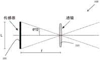
现参考图2,其示出包含硅光电倍增管(SiPM)205的示例性LiDAR设备 200,所述硅光电倍增管包括用作光学检测器的单光子雪崩光电二极管(SPAD) 的阵列。透镜210可用以提供校正光学件。对于透镜系统的给定焦距f,通过下式给出放置于焦点上且长度是L的传感器的视角θ:Referring now to FIG. 2, there is shown an

其中:in:
f是接收器透镜的焦距:f is the focal length of the receiver lens:
Lx、Ly是传感器水平和竖直长度;且Lx ,Ly are the sensor horizontal and vertical lengths; and
θx,y是SiPM检测器视角。θx,y is the SiPM detector viewing angle.
这意味着当使用短焦距时,大传感器具有大视角。当透镜有效孔径(lensaperture)变宽时,检测到更多环境光子,同时所返回的激光光子的数目保持不变。在图3中直方图窗口的起始处,如明显的大过冲所示,SiPM 205易于饱和。当SiPM 205饱和时,不再能够检测到激光光子,从而导致更低的信号检测率和更低的总SNRH。This means that a large sensor has a large viewing angle when using a short focal length. When the lens effective aperture is wider, more ambient photons are detected, while the number of returned laser photons remains the same. At the beginning of the histogram window in Figure 3, the
图4说明示例性LiDAR系统300,其包括用于通过发射透镜304发射周期性激光脉冲307的激光源305。目标308通过接收透镜310漫射并反射激光光子 312,且一些光子被反射回SiPM传感器315。SiPM传感器315将检测到的激光光子和由于噪声引起的一些检测到的光子转换成电信号,所述电信号接着由计时电子装置加时间戳。FIG. 4 illustrates an
由于传感器的必要恢复/再充电过程,因此SPAD/SiPM传感器的动态范围受限。在SiPM的微单元中的每次光检测(photo detection)中,需要通过例如电阻器来猝灭雪崩工艺,所述电阻器放出光电流并使二极管离开击穿区。接着,无源或有源再充电过程开始恢复二极管偏置电压,从而恢复准备好进行下一次光检测的初始条件。猝灭和再充电过程发生的时间量通常被称作滞后时间(dead time)或恢复时间。由于二极管的偏置条件处于盖革模式之外,因此在此时间窗口中不会发生进一步的检测。在SiPM中,当微单元进入滞后时间窗口时,其他微单元仍可检测光子。因此,微单元的数目限定传感器的光子动态范围,从而允许每单位时间检测到更高数目的光子。当由于滞后时间而导致没有微单元可用于检测时,认为SiPM处于其饱和区中。SiPM(微单元)中的较高的二极管数量对于补偿恢复过程是必要的,所述恢复过程抑制检测器的所涉及单元。由于检测器滞后时间,SiPM检测器在高环境光条件下遭遇饱和问题。The dynamic range of SPAD/SiPM sensors is limited due to the necessary recovery/recharging process of the sensor. In each photo detection in a microcell of a SiPM, the avalanche process needs to be quenched by, for example, a resistor that discharges the photocurrent and keeps the diode out of the breakdown region. Next, the passive or active recharging process begins to restore the diode bias voltage, thereby restoring the initial conditions ready for the next photodetection. The amount of time that the quenching and recharging process occurs is often referred to as the dead time or recovery time. No further detection occurs during this time window since the diode's bias condition is outside of Geiger mode. In SiPM, when a microcell enters the lag time window, other microcells can still detect photons. Thus, the number of microcells defines the photon dynamic range of the sensor, allowing a higher number of photons to be detected per unit of time. A SiPM is considered to be in its saturation region when no microcells are available for detection due to the lag time. The higher number of diodes in the SiPM (microcell) is necessary to compensate for the recovery process which suppresses the involved cells of the detector. SiPM detectors suffer from saturation issues under high ambient light conditions due to detector lag time.
参考图5和6描述SiPM传感器315的操作。SiPM传感器315包括盖革模式光电二极管315的阵列。如所说明的,猝灭电阻器320设置于可用以限制雪崩电流的每个光电二极管315附近。光电二极管315通过铝或类似导电循迹 (conductive tracking)电连接到共用偏置和接地电极。在图6中示出示意性电路,其中光电二极管315的阵列的阳极连接到共用接地电极,且所述阵列的阴极通过限流猝灭电阻器320连接到共用偏置电极以跨二极管施加偏置电压。SiPM 315 可用作根据本教导的盖革模式检测器。并不旨在将本教导限制于示例性实施例中描述的示例性盖革模式检测器,这是因为可利用其他盖革模式检测器,例如单光子雪崩二极管(SPAD)等。The operation of the
SiPM 315集成小型、电气和光学上隔离的盖革模式光电二极管315的密集阵列。每个光电二极管315串联联接到猝灭电阻器320。每个光电二极管315被称为微单元。微单元的数目通常在每平方毫米100与3000之间。随后将所有微单元的信号相加以形成SiPM 315的输出。每个微单元相同且独立地检测光子。将来自这些单独二进制检测器中的每一个的放电电流的总和组合以形成准模拟输出,并且能够给出关于入射光子通量的量值(magnitude)的信息。The
每当微单元经历盖革击穿时,每个微单元产生高度均匀且量子化的电荷量。微单元(以及因此检测器)的增益定义为输出电荷与电子上的电荷的比。可根据过电压和微单元电容而计算输出电荷。Whenever a microcell undergoes Geiger breakdown, each microcell generates a highly uniform and quantized amount of charge. The gain of the microcell (and thus the detector) is defined as the ratio of the output charge to the charge on the electrons. The output charge can be calculated from overvoltage and microcell capacitance.

其中:in:
G是微单元的增益;G is the gain of the micro-unit;
C是微单元的电容;C is the capacitance of the micro-unit;
ΔV是过电压;且ΔV is the overvoltage; and
q是电子的电荷。q is the charge of the electron.
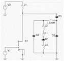
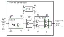
参考图7,说明了示例性激光驱动器电路700,所述激光驱动器电路鉴于其短输出脉冲而特别适用于LiDAR应用。电压源V1施加纳秒量级的短脉冲以闭合通常断开的开关S1。理想情况下,电压源V1的上升沿和下降沿具有无限转换速率,以瞬时接通开关S1。当开关S1闭合时,接着将电压V2施加到电感器 L1,所述电压在示例性实施例中可在10V到50V的范围内。通过L1的电流无法瞬间改变,这是因为要发生这种情况,电流将需要在零时间内改变有限的量。电流变化率di/dt需要无穷大,因此使得感应EMF也是无限的。不存在无限电压。因此,在电感器L1上产生自感应EMF,并通过法拉第方程式确定自感应EMF:Referring to FIG. 7, an exemplary
VL=-Ldi/dt。VL=-Ldi/dt.
自感应EMF与所施加电压V2相反,直到电流达到稳态DC值为止。由于电感器和开关永远无法完美并且总是具有一定水平的电阻,因此所施加电压、L1的电阻和闭合开关的电阻产生DC电流。The self-induced EMF opposes the applied voltage V2 until the current reaches the steady state DC value. Since inductors and switches are never perfect and always have a certain level of resistance, the applied voltage, the resistance of L1 and the resistance of the closed switch produce a DC current.
在经过在示例性布置中是数纳秒的一段时间之后,开关S1断开且通过开关 S1的到接地的路径变为高阻抗。流经电感器L1的DC电流不能突然停止,因此跨越L1产生反EMF,且电流被转移通过DC电流阻隔电容器C1和激光二极管 D1。电感器L1和电容器C1形成频率为1/(2π(LC)1/2)的谐振电路,所述频率与通过DC阻隔电容器C1注入激光二极管D1中的电流脉冲的脉冲宽度有关。适当地选择电感器L1和电容器C1的值允许调谐脉冲宽度以实现期望宽度。所产生DC电流向激光二极管D1提供驱动电流。After a period of time, which is nanoseconds in the exemplary arrangement, switch S1 opens and the path through switch S1 to ground becomes high impedance. The DC current flowing through the inductor L1 cannot stop suddenly, so a back EMF is generated across L1 and the current is diverted through the DC current blocking capacitor C1 and the laser diode D1. Inductor L1 and capacitor C1 form a resonant circuit with a frequency of 1/(2π(LC)1/2 ), which frequency is related to the pulse width of the current pulse injected into laser diode D1 through DC blocking capacitor C1. Proper selection of the values of inductor L1 and capacitor C1 allows the pulse width to be tuned to achieve the desired width. The generated DC current supplies the drive current to the laser diode D1.
本领域技术人员将理解,在激光二极管中,激光束的输出脉冲宽度不一定等于驱动电流脉冲宽度。当LC电路谐振时,二极管D2保护激光二极管免受相反极性,从而使由谐振电路引发的负向电压衰减。在理想LC电路中,将在L1 与C1之间连续循环能量。Those skilled in the art will understand that in a laser diode, the output pulse width of the laser beam is not necessarily equal to the drive current pulse width. When the LC circuit resonates, diode D2 protects the laser diode from reverse polarity, thereby attenuating the negative voltage induced by the resonant circuit. In an ideal LC circuit, energy would be continuously circulated between L1 and C1.
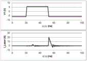
参考图8的示例性时序图,其仅作为示例提供,并且不旨在将本教导限制于所提供示例性图表。使用激光驱动器电路700来产生图8的时序图,所述激光驱动器电路使用激光二极管D1和保护二极管D2的理想二极管、具有低等效串联电阻(ESR)和L1的理想电容器C1。在t=10ns时,源V1变为5V以闭合开关S1。当S1闭合时,在L1中产生反EMF,且V_Switch在V2偏置电压下从其初始状态接地。提供第一探针(first probe)I_Switch来测量通过开关S1的电流。提供第二探针V_Switch来测量跨越开关S1的电压。提供第三探针 V_Laser来测量跨越激光二极管D1的电压。提供第四探针V_Laser来测量驱动激光二极管D1的所产生的DC电流。跨越电容器C1的电压无法立即改变,因此电压V_Laser也会下降V2电压值。接着,这在保护二极管D2上施加正向偏置,且通过C1和S1发射电流脉冲。电感器L1的线圈接着开始充电,如可从 10到40ns在I_Switch上的电流斜坡中看到。当电压V1使开关S1再次断开时,通过线圈L1的电流无法立即停止。接着,能量作为感应反EMF被传递到电容器,且由L1和C1形成的LC电路开始谐振,从而将电流脉冲传递到激光二极管D1和保护二极管D2。Reference is made to the exemplary timing diagram of FIG. 8, which is provided by way of example only, and is not intended to limit the present teachings to the exemplary diagram provided. The timing diagram of FIG. 8 is generated using a
由探针V-Switch测量的信号振荡所见的谐振的振幅随着时间的推移被电容器C1的等效串联电阻(ESR)中的能量损失衰减。由于非理想部件,电路中可能存在更多能量损失。电感器L1和开关S1将具有一些电阻,且二极管D2将通过热量损耗耗散一些功率。激光在现实中也将是非理想的,且目的是调谐电路,以使得激光在第一振荡周期内耗散大部分能量以产生光和热,从而抑制振荡。The amplitude of the resonance seen by the signal oscillations measured by the probe V-Switch is attenuated over time by energy losses in the equivalent series resistance (ESR) of capacitor C1. There may be more energy losses in the circuit due to non-ideal components. Inductor L1 and switch S1 will have some resistance, and diode D2 will dissipate some power through heat loss. The laser will also be non-ideal in reality, and the purpose is to tune the circuit so that the laser dissipates most of its energy during the first oscillation cycle to generate light and heat, thereby suppressing the oscillation.
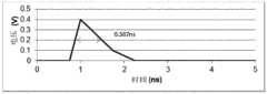
参考图9,其说明了也根据本教导的另一LiDAR设备900。LiDAR设备900 基本上类似于LiDAR设备700,且相同部件具有对应标签。LiDAR设备900中的激光二极管D1用10Ω的串联电阻模型化,以模拟激光器的功率耗散。如图 10中说明的波形展示了振荡现可通过R1中的功率耗散快速衰减,这可粗略地模型化激光二极管D1中能量转换为光和热的效果。峰值电流的值较高,而脉冲的宽度是约一纳秒。Referring to Figure 9, another
参考图11,其是基于针对S1、L1、C1和D2的商业现货部件的激光驱动器电路的SPICE模型。激光器的封装也包括于模型中,L2和L3分别代表阳极和阴极导线键合的电感,C2代表封装的并联电容,R1代表串联电阻。在图12中示出来自模型的I_laser仿真曲线。在高速MOSFET栅极驱动器上模型化脉冲源V1的上升和下降时间,例如上升和下降时间分别为1.2ns和1.4ns的Intersil ISL55110。理想情况下,这些时间是零时间长度,但最小化上升和下降时间的最实用解决方案是使用栅极驱动器。Referring to Figure 11, which is a SPICE model of the laser driver circuit based on commercial off-the-shelf parts of S1, L1, C1 and D2. The package of the laser is also included in the model, with L2 and L3 representing the inductance of the anode and cathode wire bonds, respectively, C2 the shunt capacitance of the package, and R1 the series resistance. The I_laser simulation curve from the model is shown in FIG. 12 . Model the rise and fall times of a pulsed source V1 on a high-speed MOSFET gate driver, such as the Intersil ISL55110 with rise and fall times of 1.2ns and 1.4ns, respectively. Ideally, these times are of zero duration, but the most practical solution to minimize rise and fall times is to use gate drivers.
为了获得线圈L1的快速充电,晶体管应该能够处理高电流密度并具有低导通电阻。快速关断也有利于最大化将流经激光二极管D1的峰值电流。在示例性布置中,开关S1可以由被MOSFET栅极驱动器驱动的快速氮化镓(GaN)晶体管提供,所述MOSFET栅极驱动器驱动带有具有短工作周期(例如,在10KHz 到200Mhz下10ns到100ns)的正和负脉冲(例如,±6V)的氮化镓(GaN) 晶体管S1(模型中使用的GaN系统GS66502B)。GaN晶体管优于正达到其速度、温度和功率极限的硅功率装置。GaN晶体管相比于硅的优势在于所述材料提供更高的电击穿特性、三倍的带隙和高载流子迁移率。与高功率硅替代品相比,GaN晶体管的材料和电子特性具有数个优势:To get fast charging of coil L1, the transistor should be able to handle high current density and have low on-resistance. Fast turn-off also helps maximize the peak current that will flow through laser diode D1. In an exemplary arrangement, switch S1 may be provided by a fast Gallium Nitride (GaN) transistor driven by a MOSFET gate driver with a short duty cycle (eg, 10 ns to 10 ns at 10 KHz to 200 Mhz). 100ns) positive and negative pulses (eg, ±6V) of gallium nitride (GaN) transistor S1 (GaN system GS66502B used in the model). GaN transistors are superior to silicon power devices that are reaching their speed, temperature and power limits. The advantages of GaN transistors over silicon are that the material provides higher electrical breakdown properties, a tripled band gap and high carrier mobility. The material and electronic properties of GaN transistors offer several advantages over high-power silicon alternatives:
·高介电强度·High dielectric strength
·高操作温度· High operating temperature
·高电流密度· High current density
·高速开关·High-speed switch
·低导通电阻·Low on-resistance
当S1的栅极源极电压Vgs变为正时,从S1的漏极源极路径中的电感器L1 向接地流出电流。L1由电源V2(15到40V)偏置,并在正向V1脉冲的持续时间内存储能量,通过L1的电流逐渐增加。当S1的栅极被负向驱动成-6V时,晶体管栅极源极结(Gate Source junction)被驱动为耗尽,从而导致漏极源极电流极快地关断。存储于L1上的能量接着作为尖锐的电流脉冲(sharp current pulse)通过电容器C1且作为激光驱动器电流被递送给激光二极管。图13中的仿真展示了在几纳秒的时段内获得高峰值电流(约15A)脉冲。When the gate-source voltage Vgs of S1 becomes positive, current flows from the inductor L1 in the drain-source path of S1 to ground. L1 is biased by power supply V2 (15 to 40V) and stores energy for the duration of the positive V1 pulse, the current through L1 is gradually increased. When the gate of S1 is driven negatively to -6V, the gate source junction of the transistor is driven to depletion, causing the drain source current to turn off very quickly. The energy stored on L1 is then delivered to the laser diode as a sharp current pulse through capacitor C1 and as a laser driver current. The simulation in Figure 13 shows that high peak current (about 15A) pulses are obtained over a period of several nanoseconds.
由于激光二极管通常具有数伏特的最大反向电压,因此二极管D2停止跨越激光二极管D1累积负偏置。D3的典型特性可包括低反向电流、低串联电阻和快速开关。已经发现RFPIN二极管是合适的选择。Since laser diodes typically have a maximum reverse voltage of several volts, diode D2 stops accumulating negative bias across laser diode D1. Typical characteristics of D3 can include low reverse current, low series resistance, and fast switching. RFPIN diodes have been found to be a suitable choice.
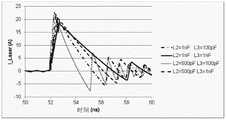
对于图11中示出的激光器模型,L2和L3表示激光器封装导线键合(laser packagewire bonds)的电感。针对图12中的仿真使用1nF的值,其表示TO18 或塑料封装部件中的短引线的电感。使用板上芯片技术或其他现有技术的封装技术,可降低封装的电感。可在阳极侧上使用多个导线键合,且可通过铜钨 (CuW)衬底将激光器的衬底阴极触点直接连接到PCB接地平面,以最小化封装电感。在图13的仿真中示出降低封装电感的效果。驱动电流的脉冲宽度减小,且峰值电流略有增大。在基于SiPM的成像LiDAR测距应用中,期望具有高峰值电流和小激光脉冲宽度。这可最大化返回光子的数目,并最小化长距离处的低反射率目标的距离不确定性。For the laser model shown in Figure 11, L2 and L3 represent the inductance of the laser package wire bonds. A value of 1 nF was used for the simulation in Figure 12, which represents the inductance of a short lead in a TO18 or plastic packaged part. Using chip-on-board technology or other state-of-the-art packaging techniques, the inductance of the package can be reduced. Multiple wire bonds can be used on the anode side, and the substrate cathode contact of the laser can be connected directly to the PCB ground plane through a copper tungsten (CuW) substrate to minimize package inductance. The effect of reducing the package inductance is shown in the simulation of FIG. 13 . The pulse width of the drive current decreases, and the peak current increases slightly. In SiPM-based imaging LiDAR ranging applications, high peak currents and small laser pulse widths are desired. This maximizes the number of returning photons and minimizes range uncertainty for low reflectivity targets at long distances.
为了实现电路,需要以正偏置和负偏置驱动晶体管的栅极,以便获得最大开关速度。在实际系统中,将需要从例如LVTTL或LVCMOS等逻辑脉冲输出导出晶体管驱动信号。图14(a)示出用于将逻辑脉冲转化为栅极驱动信号的电路实现方式的框图。V+和V-对于所选GS66502B分别是+6V和-6V,但可根据 GaN晶体管的Vgs规格而变化。调节器用于提供有关于V-轨(V-rail)的Vcc 电源供应器。Vcc通常位于V-轨上方3.3V到5V。光隔离器允许逻辑输入脉冲转换为从V-到Vcc的脉冲。接着在FET驱动器块(FET driver block)之前缓冲光隔离器输出,所述FET驱动器块再次将V-到Vcc时钟脉冲转换为在V-到V+ 的栅极驱动脉冲。FET驱动器块能够高速驱动GaN晶体管栅极,从而将双通道组合在一起以实现最大驱动能力。所使用的光隔离器是TLP117(F),且其输出由两个输出接合在一起的NC7WZ14P6X双逆变器缓冲。接着使用ISL5510IVZ来驱动晶体管栅极。To implement the circuit, the gates of the transistors need to be driven with positive and negative bias for maximum switching speed. In a real system, transistor drive signals would need to be derived from logic pulse outputs such as LVTTL or LVCMOS. Figure 14(a) shows a block diagram of a circuit implementation for converting logic pulses into gate drive signals. V+ and V- are +6V and -6V respectively for the selected GS66502B, but can vary depending on the Vgs specification of the GaN transistor. The regulator is used to provide the Vcc power supply with respect to the V-rail. Vcc is typically 3.3V to 5V above the V-rail. Opto-isolators allow logic input pulses to be converted to pulses from V- to Vcc. The opto-isolator output is then buffered before the FET driver block, which again converts the V- to Vcc clock pulses to gate drive pulses at V- to V+. The FET driver block is capable of driving GaN transistor gates at high speed, combining dual channels for maximum drive capability. The opto-isolator used is a TLP117(F) and its output is buffered by an NC7WZ14P6X dual inverter with the two outputs spliced together. Then use the ISL5510IVZ to drive the transistor gate.
图14(b)中示出的电路用作具有高峰值功率和窄脉冲宽度的脉冲激光驱动器的原型,其适用于LiDAR飞行时间(ToF)测距系统中。针对C1使用两个并联电容器,以降低快速脉冲路径到激光二极管的电感。The circuit shown in Figure 14(b) serves as a prototype for a pulsed laser driver with high peak power and narrow pulse width, which is suitable for use in LiDAR time-of-flight (ToF) ranging systems. Use two parallel capacitors for C1 to reduce the inductance of the fast pulse path to the laser diode.
参考图15,其说明了也依照本教导的另一LiDAR设备1000。LiDAR设备 1000包括如参考图7所描述的激光驱动器700和如参考图4所描述的LiDAR装置300。应理解,激光驱动器700提供用于驱动激光器305的短脉冲激光驱动器电流。在LiDAR设备1000中使用的光学检测器是以参考图5和6描述的方式操作的SiPM传感器315。Referring to Figure 15, another
参考图16,其说明通过测试OSRAM SPL PL90_3,75W,905nm,塑料封装的激光二极管获得的光脉冲的示波器屏幕截图。使用Thorlabs DET08C/M-5GHz InGaAs自由空间光电检测器来测量脉冲形状。所使用的脉冲重复率是100Khz,且结果显示实现具有785ps的脉冲。功率计用于测量平均功率,这表明激光脉冲的峰值功率约是35W。Reference is made to Figure 16, which illustrates an oscilloscope screen shot of optical pulses obtained by testing an OSRAM SPL PL90_3, 75W, 905nm, plastic packaged laser diode. Pulse shape was measured using a Thorlabs DET08C/M-5GHz InGaAs Free Space Photodetector. The pulse repetition rate used was 100Khz and the results showed that pulses with 785ps were achieved. A power meter was used to measure the average power, which indicated that the peak power of the laser pulse was about 35W.
类似的905nm激光器可从Excelitas购得,但采用降低封装引脚的电感的表面贴装封装。Excelitas TPGAD1S09H 70W SMD激光器的脉冲形状结果在图17 中示出,且可看出,脉冲宽度变为587ps,且测得峰值功率是约90W。这表明最小化激光器封装电感的优点以及其在本实用新型中的利用方式。A similar 905nm laser is available from Excelitas, but in a surface mount package that reduces the inductance of the package leads. The pulse shape results for the Excelitas TPGAD1S09H 70W SMD laser are shown in Figure 17 and it can be seen that the pulse width becomes 587ps and the measured peak power is about 90W. This demonstrates the advantages of minimizing laser package inductance and how it can be utilized in the present invention.
可调整许多参数以改变峰值功率和光脉冲宽度,L1、C1、栅极驱动脉冲的宽度、栅极偏置电压V+/V-以及线圈偏置V2是主要参数。虽然电流脉冲的宽度可能不直接对应于光脉冲宽度,但是仿真可用作用于获得所需峰值功率和脉冲的指导。Many parameters can be adjusted to vary the peak power and optical pulse width, L1, C1, the width of the gate drive pulse, gate bias voltage V+/V- and coil bias V2 are the main parameters. Although the width of the current pulse may not correspond directly to the optical pulse width, simulation can be used as a guide for obtaining the desired peak power and pulse.
参考图18,示出基本上类似于激光驱动器700的另一激光驱动器2000,且相同部件由对应标签指示。主要区别在于在激光驱动器2000中极性相比于激光驱动器700是相反的。偏置电压基准V2是负的,且二极管D1与D2的极性相反。否则,激光驱动器2000的操作以与激光驱动器700类似的方式操作。Referring to Figure 18, another
在所描述示例性实施例中,应理解,激光驱动器700可包括具有电感器L1 和DC阻隔电容器C1的谐振电路。偏置电压基准V2可以可操作地联接到电感器L1。在示例性实施例中包括开关S1的控制器可操作地控制谐振电路,以在高阻抗与低阻抗之间选择性地连接电感器L1。DC阻隔电容器C1是可操作的,用以连接到激光二极管D1。当电感器L1连接到高阻抗时,电感器L1的至少一个端子连接到开路。当电感器L1连接到低阻抗时,L1的至少一个端子被短接以接地。控制器还可包括晶体管栅极驱动器或其他控制电路,并被配置为在高阻抗与低阻抗之间重复地开关电感器L1。在示例性布置中,电感器L1具有在1nH 到50nH范围内的值,且DC阻隔电容器具有10pF到1nF范围内的值。应理解,这些示例性值仅作为示例提供,且替代值可用于电感器L1和电容器C2。由于跨越L1产生的通过电容器C1中继到激光二极管D1的反EMF电压,谐振电路产生感应激光驱动器电流。感应激光驱动器电流是具有短脉冲宽度的脉冲信号。在一个实例中,脉冲信号的每个脉冲的宽度小于或等于1ns。在另一实例中,脉冲信号的每个脉冲的宽度在100ps到2ns的范围内。控制器还可包括控制电压参考V1,其可操作来选择性地断开和闭合开关S1。控制电压参考V1是可操作的,以提供脉冲电压参考。偏置电压基准V2以10V到50V的范围内的电压电平偏置电感器L1。控制器使开关S1在断开状态与闭合状态之间重复地循环。在一个实例中,循环中的断开状态的时间段≥10纳秒。在另一实例中,循环中的闭合状态的时间段是10到100纳秒。在另一实例中,断开状态与闭合状态的时间段基本上相等。In the described exemplary embodiment, it should be understood that the
当开关S1闭合时,流经电感器的DC电流无法突然停止,由此跨越电感器 L1生成反EMF,且通过DC电流阻隔电容器C1和激光二极管D1转移由反EMF 产生的感应电流。当通过氮化镓晶体管设置开关S1时,用以驱动所述开关的栅极的脉冲信号的最大值对应于氮化镓晶体管的最大栅极源极电压范围。在一个实例中,脉冲信号在-6V到+6V的范围内。在又一个实例中,脉冲信号在-9V 到+9V的范围内。脉冲信号在10Khz到200Mhz下具有10ns到100ns的短工作周期。当晶体管被驱动成耗尽而导致漏极源极电流突然关断时,晶体管的最大反向栅极源极电压对应于栅极源极结值。存储于电感器L1上的能量接着作为尖锐的电流脉冲通过DC阻隔电容器C1且被递送给激光二极管D1。When switch S1 is closed, the DC current flowing through the inductor cannot stop abruptly, thereby generating a back EMF across inductor L1 and diverting the induced current generated by back EMF through DC current blocking capacitor C1 and laser diode D1. When the switch S1 is set by a gallium nitride transistor, the maximum value of the pulse signal used to drive the gate of the switch corresponds to the maximum gate-source voltage range of the gallium nitride transistor. In one example, the pulsed signal is in the range of -6V to +6V. In yet another example, the pulsed signal is in the range of -9V to +9V. The pulse signal has a short duty cycle of 10ns to 100ns at 10Khz to 200Mhz. The maximum reverse gate-source voltage of the transistor corresponds to the gate-source junction value when the transistor is driven into depletion causing the drain-source current to turn off abruptly. The energy stored on inductor L1 then passes through DC blocking capacitor C1 as a sharp current pulse and is delivered to laser diode D1.
应理解,图19到22的图表以图形方式示出改变电感器L1和电容器C1的值的效果。图19说明使用图7的激光驱动器的时序图,L1的值是1nH,C1的值是440pF。图20说明使用图7的激光驱动器的时序图,L1的值是10nH,C1 的值是440pF。图21说明使用图7的激光驱动器的时序图,L1的值是6nH, C1的值是10pF。图22说明使用图7的激光驱动器的时序图,L1的值是6nH, C1的值是1000pF。总激光驱动电流脉冲宽度约为谐振频率下的周期的四分之一。图23说明根据图11中的电路配置、减慢GaN晶体管的开关的效果。通过使V1的下降时间从1变化成5ns来控制GaN的开关速度。当下降时间增加且跨越开关V_Switch存在电压的相位延迟时,通过开关I_Switch减少电流所花费的时间增加。对激光器电流I_Laser的净效应(neteffect)是将峰值电流减小两倍,从而随后降低峰值光功率输出。It will be appreciated that the graphs of Figures 19 to 22 graphically illustrate the effect of varying the values of inductor L1 and capacitor C1. 19 illustrates a timing diagram using the laser driver of FIG. 7, the value of L1 is 1 nH, and the value of C1 is 440 pF. Figure 20 illustrates a timing diagram using the laser driver of Figure 7, the value of L1 is 10nH and the value of C1 is 440pF. Figure 21 illustrates a timing diagram using the laser driver of Figure 7, the value of L1 is 6nH and the value of C1 is 10pF. Figure 22 illustrates a timing diagram using the laser driver of Figure 7, the value of L1 is 6nH and the value of C1 is 1000pF. The total laser drive current pulse width is about a quarter of the period at the resonant frequency. FIG. 23 illustrates the effect of slowing down the switching of the GaN transistor according to the circuit configuration in FIG. 11 . The switching speed of GaN is controlled by varying the fall time of V1 from 1 to 5ns. As the fall time increases and there is a phase delay of the voltage across switch V_Switch, the time it takes to reduce current through switch I_Switch increases. The net effect on the laser current I_Laser is to reduce the peak current by a factor of two, thereby reducing the peak optical power output subsequently.
本领域技术人员将理解,在不脱离本实用新型的范围的情况下,可以对上述实施例进行各种修改。具体的说,应理解,图8、图10到13、图16到17和图19到23的图表仅作为示例提供,并且不旨在将本教导限制于包含于仅作为示例实例提供的这些图表中的示例性数据。以此方式,应理解,仅在根据所附权利要求认为必要的范围内限制本教导。术语半导体光电倍增器旨在覆盖任何固态光电倍增器装置,诸如硅光电倍增器[SiPM]、微像素光子计数器[MPPC]、微像素雪崩光电二极管[MAPD],但不限于此。Those skilled in the art will appreciate that various modifications may be made to the above-described embodiments without departing from the scope of the present invention. In particular, it should be understood that the graphs of FIGS. 8, 10-13, 16-17, and 19-23 are provided by way of example only, and are not intended to limit the present teachings to include those graphs provided by way of example only Example data in . In this manner, it is to be understood that the present teachings are to be limited only to the extent deemed necessary in accordance with the appended claims. The term semiconductor photomultiplier is intended to cover any solid state photomultiplier device, such as, but not limited to, silicon photomultiplier [SiPM], micropixel photon counter [MPPC], micropixel avalanche photodiode [MAPD].
类似地,当在说明书中使用时,措辞“包括”用于指出存在所述特征、整数、步骤或部件,但不排除存在或添加一个或多个附加特征、整数、步骤、部件或其群组。Similarly, when used in the specification, the word "comprising" is used to indicate the presence of stated features, integers, steps or components, but does not preclude the presence or addition of one or more additional features, integers, steps, components or groups thereof .
Claims (10)
Translated fromChineseApplications Claiming Priority (3)
| Application Number | Priority Date | Filing Date | Title |
|---|---|---|---|
| US15/451,905 | 2017-03-07 | ||
| US15/451,905US10673204B2 (en) | 2017-03-07 | 2017-03-07 | Laser driver |
| PCT/EP2018/055425WO2018162456A1 (en) | 2017-03-07 | 2018-03-06 | Laser driver |
Publications (1)
| Publication Number | Publication Date |
|---|---|
| CN211295694Utrue CN211295694U (en) | 2020-08-18 |
Family
ID=61628322
Family Applications (1)
| Application Number | Title | Priority Date | Filing Date |
|---|---|---|---|
| CN201890000589.7UActiveCN211295694U (en) | 2017-03-07 | 2018-03-06 | Laser drivers and LiDAR devices |
Country Status (3)
| Country | Link |
|---|---|
| US (1) | US10673204B2 (en) |
| CN (1) | CN211295694U (en) |
| WO (1) | WO2018162456A1 (en) |
Cited By (1)
| Publication number | Priority date | Publication date | Assignee | Title |
|---|---|---|---|---|
| CN115917896A (en)* | 2020-09-08 | 2023-04-04 | 斯兰纳亚洲有限公司 | Configurable Pulsed Laser Diode Driver |
Families Citing this family (47)
| Publication number | Priority date | Publication date | Assignee | Title |
|---|---|---|---|---|
| US10627490B2 (en) | 2016-01-31 | 2020-04-21 | Velodyne Lidar, Inc. | Multiple pulse, LIDAR based 3-D imaging |
| WO2017210418A1 (en) | 2016-06-01 | 2017-12-07 | Velodyne Lidar, Inc. | Multiple pixel scanning lidar |
| US11025031B2 (en) | 2016-11-29 | 2021-06-01 | Leonardo Electronics Us Inc. | Dual junction fiber-coupled laser diode and related methods |
| EP3593166B1 (en)* | 2017-03-31 | 2024-04-17 | Velodyne Lidar USA, Inc. | Integrated lidar illumination power control |
| CN110809704B (en) | 2017-05-08 | 2022-11-01 | 威力登激光雷达美国有限公司 | LIDAR data acquisition and control |
| EP3837743A4 (en)* | 2018-08-13 | 2022-05-18 | Leonardo Electronics US Inc. | USING A METAL-CORE Printed Circuit Board (PCB) TO CREATE AN ULTRA-THIN, HIGH-CURRENT PULSE DRIVER |
| US11056854B2 (en) | 2018-08-14 | 2021-07-06 | Leonardo Electronics Us Inc. | Laser assembly and related methods |
| US10712434B2 (en) | 2018-09-18 | 2020-07-14 | Velodyne Lidar, Inc. | Multi-channel LIDAR illumination driver |
| WO2020105145A1 (en)* | 2018-11-21 | 2020-05-28 | 三菱電機株式会社 | Optical module |
| US10826269B2 (en)* | 2018-12-24 | 2020-11-03 | Beijing Voyager Technology Co., Ltd. | Multi-pulse generation for pulsed laser diodes using low-side drivers |
| US11885958B2 (en) | 2019-01-07 | 2024-01-30 | Velodyne Lidar Usa, Inc. | Systems and methods for a dual axis resonant scanning mirror |
| US11296481B2 (en) | 2019-01-09 | 2022-04-05 | Leonardo Electronics Us Inc. | Divergence reshaping array |
| US11211421B2 (en) | 2019-01-23 | 2021-12-28 | Omnivision Technologies, Inc. | Sensor comprising gate modulation with inductor to form a resonant circuit |
| CN112868148B (en) | 2019-03-01 | 2025-08-26 | 英飞凌科技加拿大公司 | Fast-Pulse, High-Current Laser Driver |
| US11808892B2 (en)* | 2019-04-19 | 2023-11-07 | Lumentum Operations Llc | Methods for driving optical loads and driver circuits for optical loads |
| US11752571B1 (en) | 2019-06-07 | 2023-09-12 | Leonardo Electronics Us Inc. | Coherent beam coupler |
| FR3097332A1 (en)* | 2019-06-11 | 2020-12-18 | STMicroelectronics (Alps) SAS | High speed, high power optical light emitter drive circuit |
| US11876346B2 (en)* | 2019-06-26 | 2024-01-16 | Analog Devices, Inc. | Continuous wave laser driver with energy recycling |
| EP3994773A4 (en)* | 2019-07-02 | 2023-07-12 | OMRON Corporation | Electronics driver for pulsed discharge |
| US11070026B2 (en) | 2019-07-19 | 2021-07-20 | Analog Devices International Unlimited Company | High current nanosecond laser driver circuit with wide pulse-width adjustment range |
| US11075502B2 (en) | 2019-08-29 | 2021-07-27 | Analog Devices, Inc. | Laser diode driver circuit techniques |
| EP3792683A1 (en) | 2019-09-16 | 2021-03-17 | Leonardo Electronics US Inc. | Asymmetric input intensity hexagonal homogenizer |
| US11342725B2 (en)* | 2019-10-17 | 2022-05-24 | Artilux, Inc. | Light emission apparatus |
| US12334709B2 (en) | 2019-10-17 | 2025-06-17 | Artilux, Inc. | Light emission apparatus |
| WO2021079611A1 (en)* | 2019-10-23 | 2021-04-29 | ローム株式会社 | Laser diode drive circuit |
| CN111103574B (en)* | 2019-11-25 | 2025-09-30 | 上海禾赛科技有限公司 | Multi-channel driving system, laser radar including the same, and laser driving method |
| US11378663B2 (en) | 2019-11-26 | 2022-07-05 | Waymo Llc | Systems and methods for biasing light detectors |
| US11050416B1 (en)* | 2020-03-03 | 2021-06-29 | Invensense, Inc. | Implementing process, voltage, and/or temperature-insensitive resistance in complementary metal-oxide-semiconductors using a short-duty-clock cycle |
| US11870215B2 (en)* | 2020-03-23 | 2024-01-09 | Lumentum Operations Llc | Reconfigurable laser pulse generating circuit |
| CN115336124A (en)* | 2020-03-25 | 2022-11-11 | 斯兰纳亚洲有限公司 | Pulsed Laser Diode Drivers |
| DE112020006729T5 (en)* | 2020-04-15 | 2022-12-01 | Murata Manufacturing Co., Ltd. | LASER DIODE DRIVER CIRCUIT |
| US11789129B2 (en)* | 2020-07-07 | 2023-10-17 | Lumentum Operations Llc | Rectangular pulse driving circuit using cathode pre-charge and cathode-pull compensation |
| CN114076932B (en)* | 2020-08-12 | 2025-09-05 | 上海禾赛科技有限公司 | Driving device and method for laser radar light emitting device and laser radar |
| US12061291B2 (en)* | 2021-01-11 | 2024-08-13 | Beijing Voyager Technology Co., Ltd. | Systems and methods for controlling laser power in light detection and ranging (LiDAR) systems |
| US12366638B2 (en)* | 2021-03-22 | 2025-07-22 | Lumentum Operations Llc | Driver circuit for an addressable array of optical emitters |
| KR20230170011A (en) | 2021-04-12 | 2023-12-18 | 실라나 아시아 피티이 리미티드 | Pulsed Resonant Laser Diode Array Driver |
| CN113504534B (en)* | 2021-09-08 | 2021-12-07 | 柯泰光芯(常州)测试技术有限公司 | TRTF performance test system of TOF laser and working method thereof |
| US20230112690A1 (en)* | 2021-10-08 | 2023-04-13 | Lumentum Operations Llc | Driver circuit with a signal output |
| US11894656B2 (en) | 2022-03-03 | 2024-02-06 | Silanna Asia Pte Ltd | Configurable high-frequency pulsed laser diode driver |
| US12431686B2 (en) | 2022-04-05 | 2025-09-30 | Silanna Asia Pte Ltd | Single-FET pulsed laser diode driver |
| US11901697B2 (en) | 2022-04-05 | 2024-02-13 | Silanna Asia Pte Ltd | Single-FET pulsed laser diode driver |
| JP2023181772A (en)* | 2022-06-13 | 2023-12-25 | 株式会社デンソー | Light emitting unit and optical sensor |
| US12438338B2 (en) | 2022-10-03 | 2025-10-07 | Silanna Asia Pte Ltd | Auto flux timing for current resonant laser diode driver |
| US20240213741A1 (en)* | 2022-12-22 | 2024-06-27 | Silanna Asia Pte Ltd | Die-level current resonant laser diode driver |
| DE102023127718A1 (en) | 2023-10-11 | 2025-04-17 | Sick Ag | Electronic circuit and laser scanner |
| DE202023105869U1 (en) | 2023-10-11 | 2025-01-14 | Sick Ag | Electronic circuit and laser scanner |
| WO2025168409A1 (en)* | 2024-02-06 | 2025-08-14 | Ams-Osram International Gmbh | Laser device and method of operating a semiconductor laser |
Family Cites Families (23)
| Publication number | Priority date | Publication date | Assignee | Title |
|---|---|---|---|---|
| JPS5338154B2 (en)* | 1973-08-24 | 1978-10-13 | ||
| US6469357B1 (en)* | 1994-03-23 | 2002-10-22 | Agere Systems Guardian Corp. | Article comprising an oxide layer on a GaAs or GaN-based semiconductor body |
| US5822343A (en)* | 1994-08-26 | 1998-10-13 | Psc Inc. | Operating and control system for lasers useful in bar code scanners |
| DE19546563C2 (en) | 1995-12-13 | 1997-09-18 | Leica Ag | Power supply for a pulse output stage |
| US7028899B2 (en)* | 1999-06-07 | 2006-04-18 | Metrologic Instruments, Inc. | Method of speckle-noise pattern reduction and apparatus therefore based on reducing the temporal-coherence of the planar laser illumination beam before it illuminates the target object by applying temporal phase modulation techniques during the transmission of the plib towards the target |
| US7545839B2 (en) | 2003-01-02 | 2009-06-09 | Optiswitch Technology Corporation | Apparatus and method for driving a pulsed laser diode |
| US20040245592A1 (en) | 2003-05-01 | 2004-12-09 | Yale University | Solid state microchannel plate photodetector |
| JP5345383B2 (en) | 2005-04-22 | 2013-11-20 | コーニンクレッカ フィリップス エヌ ヴェ | Detector pixel, radiation detector and method, positron emission tomography system, imaging detector and calibration method thereof, detector cell invalidation method |
| RU2416840C2 (en) | 2006-02-01 | 2011-04-20 | Конинклейке Филипс Электроникс, Н.В. | Avalanche photodiode in geiger counter mode |
| JP2008287165A (en) | 2007-05-21 | 2008-11-27 | Konica Minolta Medical & Graphic Inc | Radiographic image reading apparatus |
| DE102007024074B4 (en) | 2007-05-22 | 2022-09-15 | Leica Microsystems Cms Gmbh | microscope |
| US7652257B2 (en) | 2007-06-15 | 2010-01-26 | General Electric Company | Structure of a solid state photomultiplier |
| GB2451678A (en) | 2007-08-10 | 2009-02-11 | Sensl Technologies Ltd | Silicon photomultiplier circuitry for minimal onset and recovery times |
| JP2011501189A (en) | 2007-10-25 | 2011-01-06 | ザ・リサーチ・ファウンデーション・オブ・ステイト・ユニバーシティー・オブ・ニューヨーク | Single photon spectrometer |
| AU2008318371B2 (en) | 2007-11-02 | 2013-10-17 | University Of Washington | Data acquisition for positron emission tomography |
| US7956332B2 (en) | 2008-10-29 | 2011-06-07 | General Electric Company | Multi-layer radiation detector assembly |
| US8110806B2 (en) | 2008-10-31 | 2012-02-07 | General Electric Company | Solid-state photomultiplier having improved timing resolution |
| WO2010052674A2 (en) | 2008-11-07 | 2010-05-14 | Nxp B.V. | Analog silicon photomultiplier using phase detection |
| EP2376942B1 (en) | 2008-12-15 | 2013-03-27 | Koninklijke Philips Electronics N.V. | Temperature compensation circuit for silicon photomultipliers and other single photon counters |
| EP2446301B1 (en) | 2009-06-22 | 2018-08-01 | Toyota Motor Europe | Pulsed light optical rangefinder |
| GB201004922D0 (en) | 2010-03-24 | 2010-05-12 | Sensl Technologies Ltd | Silicon photomultiplier and readout method |
| US9185762B2 (en)* | 2013-04-19 | 2015-11-10 | Infineon Technologies Ag | Time of flight illumination circuit |
| JP6738129B2 (en)* | 2015-07-28 | 2020-08-12 | 株式会社東芝 | Photodetector and lidar device using the same |
- 2017
- 2017-03-07USUS15/451,905patent/US10673204B2/enactiveActive
- 2018
- 2018-03-06WOPCT/EP2018/055425patent/WO2018162456A1/ennot_activeCeased
- 2018-03-06CNCN201890000589.7Upatent/CN211295694U/enactiveActive
Cited By (1)
| Publication number | Priority date | Publication date | Assignee | Title |
|---|---|---|---|---|
| CN115917896A (en)* | 2020-09-08 | 2023-04-04 | 斯兰纳亚洲有限公司 | Configurable Pulsed Laser Diode Driver |
Also Published As
| Publication number | Publication date |
|---|---|
| US20180261975A1 (en) | 2018-09-13 |
| WO2018162456A1 (en) | 2018-09-13 |
| US10673204B2 (en) | 2020-06-02 |
Similar Documents
| Publication | Publication Date | Title |
|---|---|---|
| CN211295694U (en) | Laser drivers and LiDAR devices | |
| US20210066885A1 (en) | Laser diode driver circuit techniques | |
| US12176679B2 (en) | Fast pulse, high current laser drivers | |
| US10852437B2 (en) | High dynamic range analog front-end receiver for long range LIDAR | |
| CN109378704B (en) | Circuit and method for driving a laser diode | |
| Kostamovaara et al. | On laser ranging based on high-speed/energy laser diode pulses and single-photon detection techniques | |
| US9985163B2 (en) | Single photon avalanche diode having pulse shaping filter | |
| CN111936885B (en) | Optical distance measuring device | |
| Nissinen et al. | A high repetition rate CMOS driver for high-energy sub-ns laser pulse generation in SPAD-based time-of-flight range finding | |
| Hallman et al. | A high-speed/power laser transmitter for single photon imaging applications | |
| CN211014629U (en) | Laser radar device | |
| Nissinen et al. | A 4 a peak current and 2 ns pulse width CMOS laser diode driver for high measurement rate applications | |
| US20070273862A1 (en) | Laser diode switching system | |
| Wen et al. | Large current nanosecond pulse generating circuit for driving semiconductor laser diode | |
| WO2022165821A1 (en) | Drive circuit, light-emitting unit, transmission module, sensing apparatus, and electronic device | |
| WO2022165820A1 (en) | Driving circuit, light-emitting unit, transmission module, sensing apparatus, and electronic device | |
| CN113437952A (en) | Reconfigurable laser pulse generation circuit | |
| Glaser | Optimizing performance of a pulsed laser diode driver based on a GaN FET | |
| Liu et al. | High-Frequency Pulsed Laser Driver Using Complementary GaN HEMTs | |
| Tajfar et al. | A 20 a sub-nanosecond integrated CMOS laser diode driver for high repetition rate SPAD-based direct Time-of-Flight measurements | |
| Blasco et al. | An 80 A, 2 to 25 ns configurable pulse-width integrated CMOS pulsed laser driver with on-chip mounted laser diode | |
| US20240275129A1 (en) | Laser pulser circuit with tunable transmit power | |
| US11265500B2 (en) | Photodetection apparatus, electronic apparatus and photodetection method | |
| Rigault et al. | CMOS VCSEL driver dedicated for sub-nanosecond laser pulses generation in SPAD-based time-of-flight rangefinder | |
| Lidow et al. | GaN-based solutions for cost-effective direct and indirect time-of-flight lidar transmitters are changing the way we live |
Legal Events
| Date | Code | Title | Description |
|---|---|---|---|
| GR01 | Patent grant | ||
| GR01 | Patent grant |