CN211125636U - semiconductor package - Google Patents
semiconductor packageDownload PDFInfo
- Publication number
- CN211125636U CN211125636UCN201922211559.XUCN201922211559UCN211125636UCN 211125636 UCN211125636 UCN 211125636UCN 201922211559 UCN201922211559 UCN 201922211559UCN 211125636 UCN211125636 UCN 211125636U
- Authority
- CN
- China
- Prior art keywords
- leads
- die pad
- die
- semiconductor package
- base portion
- Prior art date
- Legal status (The legal status is an assumption and is not a legal conclusion. Google has not performed a legal analysis and makes no representation as to the accuracy of the status listed.)
- Withdrawn - After Issue
Links
Images


Classifications
- H—ELECTRICITY
- H01—ELECTRIC ELEMENTS
- H01L—SEMICONDUCTOR DEVICES NOT COVERED BY CLASS H10
- H01L23/00—Details of semiconductor or other solid state devices
- H01L23/48—Arrangements for conducting electric current to or from the solid state body in operation, e.g. leads, terminal arrangements ; Selection of materials therefor
- H01L23/488—Arrangements for conducting electric current to or from the solid state body in operation, e.g. leads, terminal arrangements ; Selection of materials therefor consisting of soldered or bonded constructions
- H01L23/495—Lead-frames or other flat leads
- H01L23/49503—Lead-frames or other flat leads characterised by the die pad
- H—ELECTRICITY
- H01—ELECTRIC ELEMENTS
- H01L—SEMICONDUCTOR DEVICES NOT COVERED BY CLASS H10
- H01L21/00—Processes or apparatus adapted for the manufacture or treatment of semiconductor or solid state devices or of parts thereof
- H01L21/02—Manufacture or treatment of semiconductor devices or of parts thereof
- H01L21/04—Manufacture or treatment of semiconductor devices or of parts thereof the devices having potential barriers, e.g. a PN junction, depletion layer or carrier concentration layer
- H01L21/48—Manufacture or treatment of parts, e.g. containers, prior to assembly of the devices, using processes not provided for in a single one of the groups H01L21/18 - H01L21/326 or H10D48/04 - H10D48/07
- H01L21/4814—Conductive parts
- H01L21/4821—Flat leads, e.g. lead frames with or without insulating supports
- H01L21/4828—Etching
- H—ELECTRICITY
- H01—ELECTRIC ELEMENTS
- H01L—SEMICONDUCTOR DEVICES NOT COVERED BY CLASS H10
- H01L23/00—Details of semiconductor or other solid state devices
- H01L23/28—Encapsulations, e.g. encapsulating layers, coatings, e.g. for protection
- H01L23/31—Encapsulations, e.g. encapsulating layers, coatings, e.g. for protection characterised by the arrangement or shape
- H01L23/3107—Encapsulations, e.g. encapsulating layers, coatings, e.g. for protection characterised by the arrangement or shape the device being completely enclosed
- H01L23/3121—Encapsulations, e.g. encapsulating layers, coatings, e.g. for protection characterised by the arrangement or shape the device being completely enclosed a substrate forming part of the encapsulation
- H—ELECTRICITY
- H01—ELECTRIC ELEMENTS
- H01L—SEMICONDUCTOR DEVICES NOT COVERED BY CLASS H10
- H01L23/00—Details of semiconductor or other solid state devices
- H01L23/28—Encapsulations, e.g. encapsulating layers, coatings, e.g. for protection
- H01L23/31—Encapsulations, e.g. encapsulating layers, coatings, e.g. for protection characterised by the arrangement or shape
- H01L23/3107—Encapsulations, e.g. encapsulating layers, coatings, e.g. for protection characterised by the arrangement or shape the device being completely enclosed
- H01L23/3142—Sealing arrangements between parts, e.g. adhesion promotors
- H—ELECTRICITY
- H01—ELECTRIC ELEMENTS
- H01L—SEMICONDUCTOR DEVICES NOT COVERED BY CLASS H10
- H01L23/00—Details of semiconductor or other solid state devices
- H01L23/48—Arrangements for conducting electric current to or from the solid state body in operation, e.g. leads, terminal arrangements ; Selection of materials therefor
- H01L23/488—Arrangements for conducting electric current to or from the solid state body in operation, e.g. leads, terminal arrangements ; Selection of materials therefor consisting of soldered or bonded constructions
- H01L23/495—Lead-frames or other flat leads
- H01L23/49503—Lead-frames or other flat leads characterised by the die pad
- H01L23/49513—Lead-frames or other flat leads characterised by the die pad having bonding material between chip and die pad
- H—ELECTRICITY
- H01—ELECTRIC ELEMENTS
- H01L—SEMICONDUCTOR DEVICES NOT COVERED BY CLASS H10
- H01L23/00—Details of semiconductor or other solid state devices
- H01L23/48—Arrangements for conducting electric current to or from the solid state body in operation, e.g. leads, terminal arrangements ; Selection of materials therefor
- H01L23/488—Arrangements for conducting electric current to or from the solid state body in operation, e.g. leads, terminal arrangements ; Selection of materials therefor consisting of soldered or bonded constructions
- H01L23/495—Lead-frames or other flat leads
- H01L23/49517—Additional leads
- H01L23/4952—Additional leads the additional leads being a bump or a wire
- H—ELECTRICITY
- H01—ELECTRIC ELEMENTS
- H01L—SEMICONDUCTOR DEVICES NOT COVERED BY CLASS H10
- H01L23/00—Details of semiconductor or other solid state devices
- H01L23/48—Arrangements for conducting electric current to or from the solid state body in operation, e.g. leads, terminal arrangements ; Selection of materials therefor
- H01L23/488—Arrangements for conducting electric current to or from the solid state body in operation, e.g. leads, terminal arrangements ; Selection of materials therefor consisting of soldered or bonded constructions
- H01L23/495—Lead-frames or other flat leads
- H01L23/49541—Geometry of the lead-frame
- H01L23/49548—Cross section geometry
- H—ELECTRICITY
- H01—ELECTRIC ELEMENTS
- H01L—SEMICONDUCTOR DEVICES NOT COVERED BY CLASS H10
- H01L24/00—Arrangements for connecting or disconnecting semiconductor or solid-state bodies; Methods or apparatus related thereto
- H01L24/01—Means for bonding being attached to, or being formed on, the surface to be connected, e.g. chip-to-package, die-attach, "first-level" interconnects; Manufacturing methods related thereto
- H01L24/42—Wire connectors; Manufacturing methods related thereto
- H01L24/47—Structure, shape, material or disposition of the wire connectors after the connecting process
- H01L24/49—Structure, shape, material or disposition of the wire connectors after the connecting process of a plurality of wire connectors
- H—ELECTRICITY
- H01—ELECTRIC ELEMENTS
- H01L—SEMICONDUCTOR DEVICES NOT COVERED BY CLASS H10
- H01L24/00—Arrangements for connecting or disconnecting semiconductor or solid-state bodies; Methods or apparatus related thereto
- H01L24/73—Means for bonding being of different types provided for in two or more of groups H01L24/10, H01L24/18, H01L24/26, H01L24/34, H01L24/42, H01L24/50, H01L24/63, H01L24/71
- H—ELECTRICITY
- H01—ELECTRIC ELEMENTS
- H01L—SEMICONDUCTOR DEVICES NOT COVERED BY CLASS H10
- H01L24/00—Arrangements for connecting or disconnecting semiconductor or solid-state bodies; Methods or apparatus related thereto
- H01L24/80—Methods for connecting semiconductor or other solid state bodies using means for bonding being attached to, or being formed on, the surface to be connected
- H01L24/85—Methods for connecting semiconductor or other solid state bodies using means for bonding being attached to, or being formed on, the surface to be connected using a wire connector
- H—ELECTRICITY
- H01—ELECTRIC ELEMENTS
- H01L—SEMICONDUCTOR DEVICES NOT COVERED BY CLASS H10
- H01L2224/00—Indexing scheme for arrangements for connecting or disconnecting semiconductor or solid-state bodies and methods related thereto as covered by H01L24/00
- H01L2224/01—Means for bonding being attached to, or being formed on, the surface to be connected, e.g. chip-to-package, die-attach, "first-level" interconnects; Manufacturing methods related thereto
- H01L2224/26—Layer connectors, e.g. plate connectors, solder or adhesive layers; Manufacturing methods related thereto
- H01L2224/27—Manufacturing methods
- H01L2224/273—Manufacturing methods by local deposition of the material of the layer connector
- H01L2224/2733—Manufacturing methods by local deposition of the material of the layer connector in solid form
- H01L2224/27334—Manufacturing methods by local deposition of the material of the layer connector in solid form using preformed layer
- H—ELECTRICITY
- H01—ELECTRIC ELEMENTS
- H01L—SEMICONDUCTOR DEVICES NOT COVERED BY CLASS H10
- H01L2224/00—Indexing scheme for arrangements for connecting or disconnecting semiconductor or solid-state bodies and methods related thereto as covered by H01L24/00
- H01L2224/01—Means for bonding being attached to, or being formed on, the surface to be connected, e.g. chip-to-package, die-attach, "first-level" interconnects; Manufacturing methods related thereto
- H01L2224/26—Layer connectors, e.g. plate connectors, solder or adhesive layers; Manufacturing methods related thereto
- H01L2224/27—Manufacturing methods
- H01L2224/274—Manufacturing methods by blanket deposition of the material of the layer connector
- H01L2224/2743—Manufacturing methods by blanket deposition of the material of the layer connector in solid form
- H01L2224/27436—Lamination of a preform, e.g. foil, sheet or layer
- H—ELECTRICITY
- H01—ELECTRIC ELEMENTS
- H01L—SEMICONDUCTOR DEVICES NOT COVERED BY CLASS H10
- H01L2224/00—Indexing scheme for arrangements for connecting or disconnecting semiconductor or solid-state bodies and methods related thereto as covered by H01L24/00
- H01L2224/01—Means for bonding being attached to, or being formed on, the surface to be connected, e.g. chip-to-package, die-attach, "first-level" interconnects; Manufacturing methods related thereto
- H01L2224/26—Layer connectors, e.g. plate connectors, solder or adhesive layers; Manufacturing methods related thereto
- H01L2224/28—Structure, shape, material or disposition of the layer connectors prior to the connecting process
- H01L2224/29—Structure, shape, material or disposition of the layer connectors prior to the connecting process of an individual layer connector
- H01L2224/29001—Core members of the layer connector
- H01L2224/29099—Material
- H01L2224/2919—Material with a principal constituent of the material being a polymer, e.g. polyester, phenolic based polymer, epoxy
- H—ELECTRICITY
- H01—ELECTRIC ELEMENTS
- H01L—SEMICONDUCTOR DEVICES NOT COVERED BY CLASS H10
- H01L2224/00—Indexing scheme for arrangements for connecting or disconnecting semiconductor or solid-state bodies and methods related thereto as covered by H01L24/00
- H01L2224/01—Means for bonding being attached to, or being formed on, the surface to be connected, e.g. chip-to-package, die-attach, "first-level" interconnects; Manufacturing methods related thereto
- H01L2224/26—Layer connectors, e.g. plate connectors, solder or adhesive layers; Manufacturing methods related thereto
- H01L2224/28—Structure, shape, material or disposition of the layer connectors prior to the connecting process
- H01L2224/29—Structure, shape, material or disposition of the layer connectors prior to the connecting process of an individual layer connector
- H01L2224/29001—Core members of the layer connector
- H01L2224/29099—Material
- H01L2224/29198—Material with a principal constituent of the material being a combination of two or more materials in the form of a matrix with a filler, i.e. being a hybrid material, e.g. segmented structures, foams
- H01L2224/29199—Material of the matrix
- H01L2224/29294—Material of the matrix with a principal constituent of the material being a liquid not provided for in groups H01L2224/292 - H01L2224/29291
- H—ELECTRICITY
- H01—ELECTRIC ELEMENTS
- H01L—SEMICONDUCTOR DEVICES NOT COVERED BY CLASS H10
- H01L2224/00—Indexing scheme for arrangements for connecting or disconnecting semiconductor or solid-state bodies and methods related thereto as covered by H01L24/00
- H01L2224/01—Means for bonding being attached to, or being formed on, the surface to be connected, e.g. chip-to-package, die-attach, "first-level" interconnects; Manufacturing methods related thereto
- H01L2224/26—Layer connectors, e.g. plate connectors, solder or adhesive layers; Manufacturing methods related thereto
- H01L2224/28—Structure, shape, material or disposition of the layer connectors prior to the connecting process
- H01L2224/29—Structure, shape, material or disposition of the layer connectors prior to the connecting process of an individual layer connector
- H01L2224/29001—Core members of the layer connector
- H01L2224/29099—Material
- H01L2224/29198—Material with a principal constituent of the material being a combination of two or more materials in the form of a matrix with a filler, i.e. being a hybrid material, e.g. segmented structures, foams
- H01L2224/29298—Fillers
- H01L2224/29299—Base material
- H01L2224/2939—Base material with a principal constituent of the material being a polymer, e.g. polyester, phenolic based polymer, epoxy
- H—ELECTRICITY
- H01—ELECTRIC ELEMENTS
- H01L—SEMICONDUCTOR DEVICES NOT COVERED BY CLASS H10
- H01L2224/00—Indexing scheme for arrangements for connecting or disconnecting semiconductor or solid-state bodies and methods related thereto as covered by H01L24/00
- H01L2224/01—Means for bonding being attached to, or being formed on, the surface to be connected, e.g. chip-to-package, die-attach, "first-level" interconnects; Manufacturing methods related thereto
- H01L2224/26—Layer connectors, e.g. plate connectors, solder or adhesive layers; Manufacturing methods related thereto
- H01L2224/31—Structure, shape, material or disposition of the layer connectors after the connecting process
- H01L2224/32—Structure, shape, material or disposition of the layer connectors after the connecting process of an individual layer connector
- H01L2224/321—Disposition
- H01L2224/32151—Disposition the layer connector connecting between a semiconductor or solid-state body and an item not being a semiconductor or solid-state body, e.g. chip-to-substrate, chip-to-passive
- H01L2224/32221—Disposition the layer connector connecting between a semiconductor or solid-state body and an item not being a semiconductor or solid-state body, e.g. chip-to-substrate, chip-to-passive the body and the item being stacked
- H01L2224/32245—Disposition the layer connector connecting between a semiconductor or solid-state body and an item not being a semiconductor or solid-state body, e.g. chip-to-substrate, chip-to-passive the body and the item being stacked the item being metallic
- H—ELECTRICITY
- H01—ELECTRIC ELEMENTS
- H01L—SEMICONDUCTOR DEVICES NOT COVERED BY CLASS H10
- H01L2224/00—Indexing scheme for arrangements for connecting or disconnecting semiconductor or solid-state bodies and methods related thereto as covered by H01L24/00
- H01L2224/01—Means for bonding being attached to, or being formed on, the surface to be connected, e.g. chip-to-package, die-attach, "first-level" interconnects; Manufacturing methods related thereto
- H01L2224/42—Wire connectors; Manufacturing methods related thereto
- H01L2224/44—Structure, shape, material or disposition of the wire connectors prior to the connecting process
- H01L2224/45—Structure, shape, material or disposition of the wire connectors prior to the connecting process of an individual wire connector
- H01L2224/45001—Core members of the connector
- H01L2224/45099—Material
- H—ELECTRICITY
- H01—ELECTRIC ELEMENTS
- H01L—SEMICONDUCTOR DEVICES NOT COVERED BY CLASS H10
- H01L2224/00—Indexing scheme for arrangements for connecting or disconnecting semiconductor or solid-state bodies and methods related thereto as covered by H01L24/00
- H01L2224/01—Means for bonding being attached to, or being formed on, the surface to be connected, e.g. chip-to-package, die-attach, "first-level" interconnects; Manufacturing methods related thereto
- H01L2224/42—Wire connectors; Manufacturing methods related thereto
- H01L2224/47—Structure, shape, material or disposition of the wire connectors after the connecting process
- H01L2224/48—Structure, shape, material or disposition of the wire connectors after the connecting process of an individual wire connector
- H01L2224/4805—Shape
- H01L2224/4809—Loop shape
- H01L2224/48091—Arched
- H—ELECTRICITY
- H01—ELECTRIC ELEMENTS
- H01L—SEMICONDUCTOR DEVICES NOT COVERED BY CLASS H10
- H01L2224/00—Indexing scheme for arrangements for connecting or disconnecting semiconductor or solid-state bodies and methods related thereto as covered by H01L24/00
- H01L2224/01—Means for bonding being attached to, or being formed on, the surface to be connected, e.g. chip-to-package, die-attach, "first-level" interconnects; Manufacturing methods related thereto
- H01L2224/42—Wire connectors; Manufacturing methods related thereto
- H01L2224/47—Structure, shape, material or disposition of the wire connectors after the connecting process
- H01L2224/48—Structure, shape, material or disposition of the wire connectors after the connecting process of an individual wire connector
- H01L2224/481—Disposition
- H01L2224/48151—Connecting between a semiconductor or solid-state body and an item not being a semiconductor or solid-state body, e.g. chip-to-substrate, chip-to-passive
- H01L2224/48153—Connecting between a semiconductor or solid-state body and an item not being a semiconductor or solid-state body, e.g. chip-to-substrate, chip-to-passive the body and the item being arranged next to each other, e.g. on a common substrate
- H01L2224/48175—Connecting between a semiconductor or solid-state body and an item not being a semiconductor or solid-state body, e.g. chip-to-substrate, chip-to-passive the body and the item being arranged next to each other, e.g. on a common substrate the item being metallic
- H—ELECTRICITY
- H01—ELECTRIC ELEMENTS
- H01L—SEMICONDUCTOR DEVICES NOT COVERED BY CLASS H10
- H01L2224/00—Indexing scheme for arrangements for connecting or disconnecting semiconductor or solid-state bodies and methods related thereto as covered by H01L24/00
- H01L2224/01—Means for bonding being attached to, or being formed on, the surface to be connected, e.g. chip-to-package, die-attach, "first-level" interconnects; Manufacturing methods related thereto
- H01L2224/42—Wire connectors; Manufacturing methods related thereto
- H01L2224/47—Structure, shape, material or disposition of the wire connectors after the connecting process
- H01L2224/48—Structure, shape, material or disposition of the wire connectors after the connecting process of an individual wire connector
- H01L2224/481—Disposition
- H01L2224/48151—Connecting between a semiconductor or solid-state body and an item not being a semiconductor or solid-state body, e.g. chip-to-substrate, chip-to-passive
- H01L2224/48221—Connecting between a semiconductor or solid-state body and an item not being a semiconductor or solid-state body, e.g. chip-to-substrate, chip-to-passive the body and the item being stacked
- H01L2224/48245—Connecting between a semiconductor or solid-state body and an item not being a semiconductor or solid-state body, e.g. chip-to-substrate, chip-to-passive the body and the item being stacked the item being metallic
- H01L2224/48247—Connecting between a semiconductor or solid-state body and an item not being a semiconductor or solid-state body, e.g. chip-to-substrate, chip-to-passive the body and the item being stacked the item being metallic connecting the wire to a bond pad of the item
- H—ELECTRICITY
- H01—ELECTRIC ELEMENTS
- H01L—SEMICONDUCTOR DEVICES NOT COVERED BY CLASS H10
- H01L2224/00—Indexing scheme for arrangements for connecting or disconnecting semiconductor or solid-state bodies and methods related thereto as covered by H01L24/00
- H01L2224/73—Means for bonding being of different types provided for in two or more of groups H01L2224/10, H01L2224/18, H01L2224/26, H01L2224/34, H01L2224/42, H01L2224/50, H01L2224/63, H01L2224/71
- H01L2224/732—Location after the connecting process
- H01L2224/73251—Location after the connecting process on different surfaces
- H01L2224/73265—Layer and wire connectors
- H—ELECTRICITY
- H01—ELECTRIC ELEMENTS
- H01L—SEMICONDUCTOR DEVICES NOT COVERED BY CLASS H10
- H01L2224/00—Indexing scheme for arrangements for connecting or disconnecting semiconductor or solid-state bodies and methods related thereto as covered by H01L24/00
- H01L2224/80—Methods for connecting semiconductor or other solid state bodies using means for bonding being attached to, or being formed on, the surface to be connected
- H01L2224/83—Methods for connecting semiconductor or other solid state bodies using means for bonding being attached to, or being formed on, the surface to be connected using a layer connector
- H01L2224/831—Methods for connecting semiconductor or other solid state bodies using means for bonding being attached to, or being formed on, the surface to be connected using a layer connector the layer connector being supplied to the parts to be connected in the bonding apparatus
- H01L2224/83101—Methods for connecting semiconductor or other solid state bodies using means for bonding being attached to, or being formed on, the surface to be connected using a layer connector the layer connector being supplied to the parts to be connected in the bonding apparatus as prepeg comprising a layer connector, e.g. provided in an insulating plate member
- H—ELECTRICITY
- H01—ELECTRIC ELEMENTS
- H01L—SEMICONDUCTOR DEVICES NOT COVERED BY CLASS H10
- H01L2224/00—Indexing scheme for arrangements for connecting or disconnecting semiconductor or solid-state bodies and methods related thereto as covered by H01L24/00
- H01L2224/80—Methods for connecting semiconductor or other solid state bodies using means for bonding being attached to, or being formed on, the surface to be connected
- H01L2224/83—Methods for connecting semiconductor or other solid state bodies using means for bonding being attached to, or being formed on, the surface to be connected using a layer connector
- H01L2224/8319—Arrangement of the layer connectors prior to mounting
- H01L2224/83191—Arrangement of the layer connectors prior to mounting wherein the layer connectors are disposed only on the semiconductor or solid-state body
- H—ELECTRICITY
- H01—ELECTRIC ELEMENTS
- H01L—SEMICONDUCTOR DEVICES NOT COVERED BY CLASS H10
- H01L2224/00—Indexing scheme for arrangements for connecting or disconnecting semiconductor or solid-state bodies and methods related thereto as covered by H01L24/00
- H01L2224/80—Methods for connecting semiconductor or other solid state bodies using means for bonding being attached to, or being formed on, the surface to be connected
- H01L2224/83—Methods for connecting semiconductor or other solid state bodies using means for bonding being attached to, or being formed on, the surface to be connected using a layer connector
- H01L2224/8319—Arrangement of the layer connectors prior to mounting
- H01L2224/83192—Arrangement of the layer connectors prior to mounting wherein the layer connectors are disposed only on another item or body to be connected to the semiconductor or solid-state body
- H—ELECTRICITY
- H01—ELECTRIC ELEMENTS
- H01L—SEMICONDUCTOR DEVICES NOT COVERED BY CLASS H10
- H01L2224/00—Indexing scheme for arrangements for connecting or disconnecting semiconductor or solid-state bodies and methods related thereto as covered by H01L24/00
- H01L2224/80—Methods for connecting semiconductor or other solid state bodies using means for bonding being attached to, or being formed on, the surface to be connected
- H01L2224/83—Methods for connecting semiconductor or other solid state bodies using means for bonding being attached to, or being formed on, the surface to be connected using a layer connector
- H01L2224/8319—Arrangement of the layer connectors prior to mounting
- H01L2224/83193—Arrangement of the layer connectors prior to mounting wherein the layer connectors are disposed on both the semiconductor or solid-state body and another item or body to be connected to the semiconductor or solid-state body
- H—ELECTRICITY
- H01—ELECTRIC ELEMENTS
- H01L—SEMICONDUCTOR DEVICES NOT COVERED BY CLASS H10
- H01L2224/00—Indexing scheme for arrangements for connecting or disconnecting semiconductor or solid-state bodies and methods related thereto as covered by H01L24/00
- H01L2224/80—Methods for connecting semiconductor or other solid state bodies using means for bonding being attached to, or being formed on, the surface to be connected
- H01L2224/85—Methods for connecting semiconductor or other solid state bodies using means for bonding being attached to, or being formed on, the surface to be connected using a wire connector
- H—ELECTRICITY
- H01—ELECTRIC ELEMENTS
- H01L—SEMICONDUCTOR DEVICES NOT COVERED BY CLASS H10
- H01L2224/00—Indexing scheme for arrangements for connecting or disconnecting semiconductor or solid-state bodies and methods related thereto as covered by H01L24/00
- H01L2224/91—Methods for connecting semiconductor or solid state bodies including different methods provided for in two or more of groups H01L2224/80 - H01L2224/90
- H01L2224/92—Specific sequence of method steps
- H01L2224/922—Connecting different surfaces of the semiconductor or solid-state body with connectors of different types
- H01L2224/9222—Sequential connecting processes
- H01L2224/92242—Sequential connecting processes the first connecting process involving a layer connector
- H01L2224/92247—Sequential connecting processes the first connecting process involving a layer connector the second connecting process involving a wire connector
- H—ELECTRICITY
- H01—ELECTRIC ELEMENTS
- H01L—SEMICONDUCTOR DEVICES NOT COVERED BY CLASS H10
- H01L24/00—Arrangements for connecting or disconnecting semiconductor or solid-state bodies; Methods or apparatus related thereto
- H01L24/01—Means for bonding being attached to, or being formed on, the surface to be connected, e.g. chip-to-package, die-attach, "first-level" interconnects; Manufacturing methods related thereto
- H01L24/26—Layer connectors, e.g. plate connectors, solder or adhesive layers; Manufacturing methods related thereto
- H01L24/28—Structure, shape, material or disposition of the layer connectors prior to the connecting process
- H01L24/29—Structure, shape, material or disposition of the layer connectors prior to the connecting process of an individual layer connector
- H—ELECTRICITY
- H01—ELECTRIC ELEMENTS
- H01L—SEMICONDUCTOR DEVICES NOT COVERED BY CLASS H10
- H01L24/00—Arrangements for connecting or disconnecting semiconductor or solid-state bodies; Methods or apparatus related thereto
- H01L24/01—Means for bonding being attached to, or being formed on, the surface to be connected, e.g. chip-to-package, die-attach, "first-level" interconnects; Manufacturing methods related thereto
- H01L24/26—Layer connectors, e.g. plate connectors, solder or adhesive layers; Manufacturing methods related thereto
- H01L24/31—Structure, shape, material or disposition of the layer connectors after the connecting process
- H01L24/32—Structure, shape, material or disposition of the layer connectors after the connecting process of an individual layer connector
- H—ELECTRICITY
- H01—ELECTRIC ELEMENTS
- H01L—SEMICONDUCTOR DEVICES NOT COVERED BY CLASS H10
- H01L24/00—Arrangements for connecting or disconnecting semiconductor or solid-state bodies; Methods or apparatus related thereto
- H01L24/01—Means for bonding being attached to, or being formed on, the surface to be connected, e.g. chip-to-package, die-attach, "first-level" interconnects; Manufacturing methods related thereto
- H01L24/42—Wire connectors; Manufacturing methods related thereto
- H01L24/47—Structure, shape, material or disposition of the wire connectors after the connecting process
- H01L24/48—Structure, shape, material or disposition of the wire connectors after the connecting process of an individual wire connector
- H—ELECTRICITY
- H01—ELECTRIC ELEMENTS
- H01L—SEMICONDUCTOR DEVICES NOT COVERED BY CLASS H10
- H01L24/00—Arrangements for connecting or disconnecting semiconductor or solid-state bodies; Methods or apparatus related thereto
- H01L24/80—Methods for connecting semiconductor or other solid state bodies using means for bonding being attached to, or being formed on, the surface to be connected
- H01L24/83—Methods for connecting semiconductor or other solid state bodies using means for bonding being attached to, or being formed on, the surface to be connected using a layer connector
- H—ELECTRICITY
- H01—ELECTRIC ELEMENTS
- H01L—SEMICONDUCTOR DEVICES NOT COVERED BY CLASS H10
- H01L2924/00—Indexing scheme for arrangements or methods for connecting or disconnecting semiconductor or solid-state bodies as covered by H01L24/00
- H01L2924/15—Details of package parts other than the semiconductor or other solid state devices to be connected
- H01L2924/181—Encapsulation
Landscapes
- Engineering & Computer Science (AREA)
- Microelectronics & Electronic Packaging (AREA)
- Computer Hardware Design (AREA)
- Power Engineering (AREA)
- Physics & Mathematics (AREA)
- Condensed Matter Physics & Semiconductors (AREA)
- General Physics & Mathematics (AREA)
- Geometry (AREA)
- Manufacturing & Machinery (AREA)
- Lead Frames For Integrated Circuits (AREA)
Abstract
Description
Translated fromChinese技术领域technical field
本公开的实施例涉及半导体封装件。Embodiments of the present disclosure relate to semiconductor packages.
背景技术Background technique
无引线(或没有引线)封装件通常用于其中期望小尺寸封装件的应用。通常,扁平无引线封装件提供由平面引线框形成的近芯片级包封的封装件。位于封装件的底表面上的焊接区(land)提供与板(诸如印刷电路板(PCB))的电连接。许多无引线封装件(诸如方形扁平无引线(QFN)封装件)包括安装至裸片焊盘并诸如通过导电线电耦合至引线的半导体裸片或芯片。包封材料包围半导体裸片和导电线以及部分裸片焊盘和引线。包封材料保护其中的导电元件。Leadless (or leadless) packages are often used in applications where small footprint packages are desired. Typically, flat no-lead packages provide a near chip-scale encapsulated package formed from a planar leadframe. Lands on the bottom surface of the package provide electrical connection to a board, such as a printed circuit board (PCB). Many leadless packages, such as quad flat no-lead (QFN) packages, include a semiconductor die or chip mounted to a die pad and electrically coupled to leads, such as by conductive wires. The encapsulant surrounds the semiconductor die and conductive lines and portions of the die pads and leads. The encapsulating material protects the conductive elements therein.
这些封装件的制造商在保持最小规格(诸如,为了防止短路或其他电气故障的封装件中的电部件之间的距离、以及用于将封装件焊接至PCB的合适尺寸的焊接区)的同时面临着减小封装件尺寸的重大挑战。期望可满足最小规格的更小的无引线封装件。Manufacturers of these packages maintain minimum specifications, such as the distance between electrical components in the package to prevent short circuits or other electrical failures, and appropriately sized pads for soldering the package to the PCB There is a significant challenge to reduce package size. Smaller leadless packages that meet minimum specifications are desired.
实用新型内容Utility model content
为了在满足最小规格的同时进一步减小封装件的尺寸,本公开提出了一种半导体封装件。In order to further reduce the size of the package while meeting minimum specifications, the present disclosure proposes a semiconductor package.
在第一方面,提供了一种半导体封装件,该半导体封装件包括:裸片焊盘,具有内部部分和外部部分,内部部分包括内部周界部分,外部部分包括外部周界部分,内部周界部分延伸超出外部周界部分,内部周界部分包括多个突起,多个突起通过凹部彼此间隔开;半导体裸片,被耦合至裸片焊盘的内部部分;多个引线,每个引线包括上部部分和基底部分,其中引线的基底部分相对于裸片焊盘的内部周界部分的多个突起交错,使得每个基底部分面对相应的凹部;多个导电线,半导体裸片分别通过多个导电线电耦合至多个引线;以及包封材料,位于多个引线、裸片焊盘、半导体裸片和多个导电线上方,其中裸片焊盘的外部部分的表面和多个引线的基底部分的表面在半导体封装件的外表面处暴露。In a first aspect, a semiconductor package is provided, the semiconductor package including a die pad having an inner portion and an outer portion, the inner portion including an inner perimeter portion, the outer portion including an outer perimeter portion, the inner perimeter a portion extending beyond the outer perimeter portion, the inner perimeter portion including a plurality of protrusions spaced apart from each other by the recess; a semiconductor die coupled to the inner portion of the die pad; a plurality of leads, each lead including an upper portion portion and base portion, wherein the base portion of the lead is staggered relative to the plurality of protrusions of the inner perimeter portion of the die pad such that each base portion faces a corresponding recess; a plurality of conductive lines, the semiconductor die respectively passing through a plurality of a conductive line electrically coupled to the plurality of leads; and an encapsulation material over the plurality of leads, the die pad, the semiconductor die, and the plurality of conductive lines, wherein a surface of an outer portion of the die pad and a base portion of the plurality of leads The surface of the semiconductor package is exposed at the outer surface of the semiconductor package.
根据一个实施例,多个引线的上部部分具有在相邻引线之间延伸的第一宽度,多个引线的基底部分具有在相邻引线之间延伸的第二宽度,其中第二宽度小于第一宽度。According to one embodiment, upper portions of the plurality of leads have a first width extending between adjacent leads, and base portions of the plurality of leads have a second width extending between adjacent leads, wherein the second width is less than the first width width.
根据一个实施例,多个引线的上部部分延伸超出基底部分的相对侧,形成引线锁,引线锁帮助将多个引线锁定在包封材料中。According to one embodiment, upper portions of the plurality of leads extend beyond opposite sides of the base portion, forming lead locks that assist in locking the plurality of leads within the encapsulation material.
根据一个实施例,多个引线的上部部分通过中心部分与基底部分间隔开,其中中心部分在宽度方向上具有与上部部分相同的宽度。According to one embodiment, the upper portion of the plurality of leads is spaced apart from the base portion by a central portion, wherein the central portion has the same width in the width direction as the upper portion.
根据一个实施例,多个引线的基底部分小于多个引线的总厚度的50%,其中裸片焊盘的内部周界部分小于裸片焊盘的总厚度的50%。According to one embodiment, the base portion of the plurality of leads is less than 50% of the total thickness of the plurality of leads, wherein the inner perimeter portion of the die pad is less than 50% of the total thickness of the die pad.
根据一个实施例,多个引线与裸片焊盘之间的最小距离在多个引线的基底部分与裸片焊盘的内部周界部分之间。According to one embodiment, the minimum distance between the plurality of leads and the die pad is between a base portion of the plurality of leads and an inner perimeter portion of the die pad.
根据一个实施例,每个引线和裸片焊盘之间的最小距离至少为0.15mm。According to one embodiment, the minimum distance between each lead and the die pad is at least 0.15mm.
根据一个实施例,多个突起从裸片焊盘的内部周界部分的一部分延伸。According to one embodiment, a plurality of protrusions extend from a portion of the inner perimeter portion of the die pad.
根据一个实施例,多个引线的基底部分包括中心部分,中心部分将上部部分与朝向裸片焊盘延伸超出上部部分的基底部分的表面分离。According to one embodiment, the base portion of the plurality of leads includes a central portion separating the upper portion from a surface of the base portion extending beyond the upper portion toward the die pad.
在第二方面,提供了一种半导体封装件,该半导体封装件包括:裸片焊盘,具有内部部分和外部部分,内部部分大于外部部分,其中内部部分包括沿着裸片焊盘的第一侧的多个突起,其中多个突起在相邻突起之间形成凹部;半导体裸片,被耦合至裸片焊盘的内部部分;多个引线,面对裸片焊盘的第一侧,多个引线包括上部部分和基底部分,其中多个引线的基底部分相对于裸片焊盘的内部部分的多个突起交错,其中上部部分形成引线锁,引线锁在相邻引线的方向上延伸;多个导电线,半导体裸片分别通过多个导电线电耦合至多个引线;以及包封材料,位于多个引线、裸片焊盘、半导体裸片和多个导电线上方,其中裸片焊盘的外部部分的表面和多个引线的基底部分的表面在半导体封装件的外表面处暴露。In a second aspect, a semiconductor package is provided that includes a die pad having an inner portion and an outer portion, the inner portion being larger than the outer portion, wherein the inner portion includes a first portion along the die pad a plurality of bumps on the side, wherein the plurality of bumps form recesses between adjacent bumps; a semiconductor die coupled to the inner portion of the die pad; a plurality of leads facing the first side of the die pad, a plurality of each lead includes an upper portion and a base portion, wherein the base portions of the plurality of leads are staggered relative to the plurality of protrusions of the inner portion of the die pad, wherein the upper portion forms lead locks that extend in the direction of adjacent leads; a plurality of conductive lines, the semiconductor die is electrically coupled to the plurality of leads through the plurality of conductive lines, respectively; and an encapsulation material located over the plurality of leads, the die pad, the semiconductor die and the plurality of conductive lines, wherein the die pad is The surface of the outer portion and the surface of the base portion of the plurality of leads are exposed at the outer surface of the semiconductor package.
根据一个实施例,在上部部分的相对侧,多个引线的上部部分延伸超出多个引线的基底部分。According to one embodiment, the upper portion of the plurality of leads extends beyond the base portion of the plurality of leads on the opposite side of the upper portion.
根据一个实施例,多个引线的基底部分面对裸片焊盘的外部部分,并且相对于相邻突起之间的凹部对准。According to one embodiment, the base portions of the plurality of leads face the outer portions of the die pads and are aligned relative to the recesses between adjacent bumps.
根据一个实施例,多个引线中的每个引线与裸片焊盘之间的最短距离为至少0.15mm。According to one embodiment, the shortest distance between each lead of the plurality of leads and the die pad is at least 0.15 mm.
根据一个实施例,引线锁通过多个引线的上部部分形成,上部部分具有的宽度大于多个引线的基底部分的宽度。According to one embodiment, the lead lock is formed by an upper portion of the plurality of leads, the upper portion having a width greater than the width of a base portion of the plurality of leads.
通过上述实施例,实现了可满足最小规格的、具有更小尺寸的无引线封装件。Through the above-described embodiments, a leadless package having a smaller size that can meet minimum specifications is realized.
附图说明Description of drawings
在附图中,相同的参考标号表示相似的元件。附图中元件的大小和相对位置不需要按比例绘制。In the drawings, the same reference numerals denote similar elements. The sizes and relative positions of elements in the drawings are not necessarily drawn to scale.
图1A是根据一个实施例的半导体封装件的截面图的示意图。1A is a schematic illustration of a cross-sectional view of a semiconductor package according to one embodiment.
图1B是图1A的半导体封装件在另一位置处的截面图的示意图。1B is a schematic illustration of a cross-sectional view of the semiconductor package of FIG. 1A at another location.
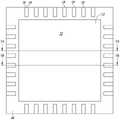
图1C是图1A的封装件的仰视图。Figure 1C is a bottom view of the package of Figure 1A.
图2A-图2D是图1的封装件的引线框的各个视图的示意图。2A-2D are schematic diagrams of various views of the leadframe of the package of FIG. 1 .
图3A-图3F是示出根据一个实施例的图1A的引线框半导体封装件的制造阶段的截面图。3A-3F are cross-sectional views illustrating stages of manufacture of the leadframe semiconductor package of FIG. 1A according to one embodiment.
具体实施方式Detailed ways
总体而言,一个或多个实施例是针对一种引线框封装件,其具有多个引线、裸片焊盘、耦合至裸片焊盘的半导体裸片和包封材料。裸片焊盘的内部部分包括周界部分,周界部分包括彼此间隔开的多个突起。突起帮助将裸片焊盘锁定在包封材料中。多个引线包括上部部分和基底部分。多个引线的基底部分相对于裸片焊盘的多个突起偏移(或交错)。特别地,基底部分朝向裸片焊盘纵向延伸,并且位于相应的突起之间。引线的上部部分包括引线锁,引线锁沿相邻引线的方向延伸超出基底部分。引线锁和裸片焊盘中的突起帮助将引线和裸片焊盘锁定在包封材料中。In general, one or more embodiments are directed to a leadframe package having a plurality of leads, a die pad, a semiconductor die coupled to the die pad, and an encapsulation material. The inner portion of the die pad includes a perimeter portion that includes a plurality of protrusions spaced apart from each other. The bumps help lock the die pad in the encapsulant. The plurality of leads include an upper portion and a base portion. The base portions of the plurality of leads are offset (or staggered) with respect to the plurality of bumps of the die pad. In particular, the base portion extends longitudinally towards the die pad and is located between the corresponding protrusions. The upper portion of the leads includes lead locks that extend beyond the base portion in the direction of adjacent leads. Lead locks and bumps in the die pad help lock the leads and die pad into the encapsulant.
在以下描述中,阐述了某些特定细节以提供对所公开的主题的各个方面的透彻理解。然而,可以在没有这些具体细节的情况下实践所公开的主题。在一些情况下,不详细描述半导体处理的已知结构和方法(诸如形成半导体芯片),以避免混淆本公开的其他方面的描述。In the following description, certain specific details are set forth in order to provide a thorough understanding of various aspects of the disclosed subject matter. However, the disclosed subject matter may be practiced without these specific details. In some instances, known structures and methods of semiconductor processing, such as forming semiconductor chips, are not described in detail in order to avoid obscuring the description of other aspects of the present disclosure.
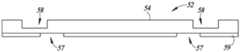
图1A和图1B示出了根据本公开的一个实施例的引线框半导体封装件10的截面图。图1C示出了封装件的底表面以及图1A和图1B的截面线的位置。1A and 1B illustrate cross-sectional views of a
封装件10是引线框封装件,其包括裸片焊盘12和位于裸片焊盘12的所有侧的多个引线14。引线14彼此间隔开,并且与裸片焊盘12间隔开。参照图1B,引线14包括上部部分16和基底部分18。如下面将要解释的,上部部分16包括帮助将引线固定在封装件本体(诸如包封材料44)内的锁定特征或锚(引线锁)。
尽管在图1C中在封装件10的每侧示出了八个引线14,但是应当理解,封装件中可以包括任意数目的引线,包括位于裸片焊盘的一侧或多侧上的一个引线。在至少一个实施例中,引线14被设置在裸片焊盘12的相对两侧。裸片焊盘12和引线14由导电材料(诸如金属材料)的引线框形成。在一个实施例中,引线框是铜或铜合金。Although eight
参考图1A和图1B,裸片焊盘12具有内部部分20和外部部分22。半导体裸片30通过粘合材料32固定至裸片焊盘12的内部部分20的表面。如本领域已知的,半导体裸片30由半导体材料(诸如硅)制成,并且包括上有源表面,该表面包括电子部件(诸如集成电路)。半导体裸片30可以结合有微机电传感器(MEMS)器件、专用集成电路(ASIC)或任何其他类型的有源结构。粘合材料32可以是被配置为适当地将半导体裸片30固定至裸片焊盘12的任何材料,诸如胶、膏、胶带等。Referring to FIGS. 1A and 1B , the
参照图1B,导电线36将半导体裸片30电耦合至引线14的上部部分16。特别地,导电线36的第一端38被耦合至半导体裸片30的接合焊盘40,并且导电线36的第二端42被耦合至引线14中的相应一个引线的上部部分16。如本领域已知的,导电线36提供半导体裸片30的电路和引线14之间的电通信。Referring to FIG. 1B ,
包封材料44位于裸片焊盘12和引线14上,并且围绕半导体裸片30和导电线36。包封材料44填充相邻引线14之间以及引线14和裸片焊盘12之间的空间。包封材料44形成封装件10的底表面以及裸片焊盘12的外部部分22的表面和引线14的基底部分18的表面。引线14的基底部分18的表面形成封装件10的焊接区。包封材料44的上表面形成封装件10的外部上表面。包封材料44的侧面以及引线14的侧面形成封装件10的外部侧面。
包封材料44是绝缘材料,其保护半导体裸片的电部件和导电线不受损害,诸如腐蚀、物理损坏、湿气损坏或其他导致电器件和材料损坏的原因。在一些实施例中,包封材料是模制材料,诸如聚合物、硅酮、树脂、聚酰亚胺或环氧树脂。The
参照图1A,裸片焊盘12的内部部分20宽于裸片焊盘12的外部部分22。即,裸片焊盘12的内部部分20的周界延伸超出裸片焊盘12的外部部分22的周界。如下文将更详细解释的,裸片焊盘12的内部部分20的周界用作帮助将裸片焊盘12保持在包封材料44内的锁定特征或锚。Referring to FIG. 1A , the
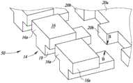
图2A是包括图1A-图1C的封装件10的裸片焊盘12和引线14的引线框50的一部分的俯视图,而图2B是引线框50的一部分的顶部等距视图。图2C是如图2B中的框所示的图2B的引线框50的截面的分解顶部等距视图,而图2D是该框截面的分解底部等距视图。2A is a top view of a portion of
在所示实施例中,引线框50由具有恒定厚度的引线框形成。因此,引线14的上部部分16的表面与裸片焊盘12的内部部分20的表面共面;并且引线14的基底部分18的表面与裸片焊盘12的外部部分22共面。In the illustrated embodiment, the
如前所述,裸片焊盘12包括内部部分20和外部部分22。从图2D更好地看出,内部部分20具有的周界20a延伸超过外部部分22。特别地,周界部分20a围绕裸片焊盘12的整个周界延伸超过外部部分22。内部部分的周界20a包括多个间隔开的突起20b。包括突起20b的周界部分20a用作帮助将裸片焊盘12保持在包封材料内的锁定特征或锚。即,当包封材料被形成在引线框50周围时,包括突起20b的周界部分20a帮助将裸片焊盘12锚定在包封材料中。As previously mentioned, the
突起20b在它们之间形成凹部。突起20b相对于引线14交错,使得引线14的基底部分18面对在周界部分20a的相邻突起20b之间形成的凹部,这从图2A可以更好地看出。因此,如图2A中的箭头A-A所示,保持引线14和裸片焊盘12之间的最小距离。在一个实施例中,引线14和裸片焊盘12之间的最小距离至少为0.15毫米(mm)。The
参考图2D,每个引线14具有:最大厚度T,从上部部分16的顶部延伸到基底部分18的底表面;最大宽度W,在相邻引线14的方向上在上部部分16中延伸;以及长度L,沿引线14的纵向轴线朝向裸片焊盘12在基底部分中延伸。上部部分16的宽度宽于基底部分18的宽度。基底部分18的长度长于上部部分16的长度。2D, each lead 14 has: a maximum thickness T, extending from the top of the
引线14的上部部分16沿其最大宽度W的方向朝向相邻引线横向突出,以形成引线锁16a。即,引线锁16a延伸超过引线14在基底部分18处的侧面,使得引线14的基底部分18在W方向上比上部部分16窄。因此,相邻引线14之间的最小距离由相邻引线锁16a之间的距离来限定。在一个实施例中,相邻引线锁16a之间的最小距离至少为0.15mm。引线锁16a用作帮助将引线14固定在包封材料内的锁定特征或锚。即,当包封材料被形成在引线框50周围时,包封材料包围引线14的上部部分16,以帮助将引线14锚定在包封材料中。The
引线14的基底部分18在从引线14朝向裸片焊盘12延伸的纵向方向上具有更大的长度L。较长的基底部分18提供用于在封装件的底表面处形成焊接区的改进表面积。关于这点,用于板级可靠性(BLR)性能的焊点可靠性因此得到提高。由于裸片焊盘12的周界部分20a的相邻突起20b之间的凹部,在不必增加封装件尺寸的情况下提供增加的焊接区。The
从图2D可以更好地看出,引线14的基底部分18中的每一个都包括将基底部分18与上部部分16间隔开一定距离的中心部分。即,中心部分将基底部分18与上部部分16分离。在所示的实施例中,每个引线14的上部部分16都具有与裸片焊盘12的周界部分20a(包括突起20b)相同的厚度T。此外,由于上部部分16和基底部分18之间的距离,由于中心部分,裸片焊盘12的周界部分20a也沿厚度T的方向与引线14的基底部分18间隔开。因此,相应引线14与裸片焊盘14之间的最小距离由如图2C中的箭头B-B所示的距离来限定。在至少一个实施例中,引线14与裸片焊盘12(在突起20b处)之间的最小距离至少为0.15mm。As can be better seen in FIG. 2D , each of the
通过使引线14的基底部分18与裸片焊盘12的周界部分20a的突起20b交错,可以减小封装件的尺寸,同时保持引线的适当尺寸的焊接区以用于耦合至另一器件。此外,形成在相邻引线的方向上延伸的引线锁也允许适当尺寸的焊接区。By staggering the
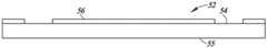
图3A-图3F示出了制造图1A-图1C的引线框半导体封装件10的各个阶段。如图3A所示,提供引线框条带52的一部分。引线框条带52是导电材料(诸如金属),并且在一些实施例中由铜或铜合金制成。尽管仅示出一个裸片焊盘和引线集合,但是引线框条带52包括多个裸片焊盘12、引线14和耦合到一起的连接杆或拉杆(tie bar)(未示出)。如本领域已知的,引线框条带52可以包括沿单行布置的裸片焊盘,或者可以包括裸片焊盘的阵列。3A-3F illustrate various stages of manufacturing the
引线框条带52包括上表面54和下表面55。在引线框条带52的上表面54上形成图案化层56。图案化层56可以是任何合适的材料,诸如光敏材料,如光阻剂。上表面54上的图案化层56包括开口,在该开口处,引线框条带52的部分将被刻蚀以形成第一凹部58,从而形成引线14的上部部分16、裸片焊盘12的突起20b,并且在上表面处将引线彼此间隔开,并且将引线和裸片焊盘间隔开。特别地,引线框条带52的上表面54在第一刻蚀步骤中被半刻蚀以形成第一凹部58。根据标准半导体处理技术,第一刻蚀步骤可以包括湿法刻蚀、干法刻蚀或它们的组合。第一凹部58可以具有大于从上表面54开始到引线框条带52的厚度的一半的深度。例如,第一凹部58可以在引线框条带的厚度的60%或70%之间延伸。在一个实施例中,凹部58延伸通过引线框条带52的厚度的60%。如图2B所示,从引线框条带52的上表面54移除图案化层56。The
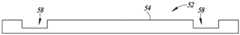
类似地,如图3C所示,在引线框条带52的下表面55上形成具有开口57的另一图案化层59,以形成如图3D所示的第二凹部60。开口57与第一凹部58的部分重叠,使得在刻蚀步骤之后形成裸片焊盘12和引线14。特别地,下表面55上的图案化层59包括开口57,在该开口57处,引线框条带52的部分将被刻蚀以形成第二凹部60。特别地,引线框条带52的下表面55在第二刻蚀步骤中被半刻蚀以形成第二凹部60。使用标准半导体处理技术,第二刻蚀步骤可以包括湿法刻蚀、干法刻蚀或它们的组合。第二凹部60延伸超过引线框条带52的厚度的一半,特别地,在厚度的60%或70%之间,更特别地,是厚度的60%。应理解,第一和第二刻蚀步骤共同刻蚀穿过至少引线框条带的整个厚度,使得在第一凹部和第二凹部之间形成通孔。Similarly, as shown in FIG. 3C, another patterned
图案化层59可以是与图案化层56相似的材料,并且在形成凹部60之后被移除。可代替地,图案化层59可以是在形成凹部60之后不被移除的图案化导电层。特别地,诸如通过电镀技术,在引线框条带52的下表面55上沉积图案化导电层。图案化导电层可以包括与引线框条带本身不同的一种或多种导电材料。例如,图案化导电层可以是一种或多种金属材料,诸如Ni/Pd/Ag、Ni/Pd/Au-Ag合金或Ni/Pd/Au/Ag。
如图3E所示,半导体裸片30通过粘合材料32(诸如胶带、膏、胶等)耦合至裸片焊盘12的表面。在将半导体裸片30放置在裸片焊盘12的表面上之前,粘合材料32可以首先被耦合至半导体裸片30、裸片焊盘12或裸片和裸片焊盘二者。As shown in FIG. 3E, the semiconductor die 30 is coupled to the surface of the
半导体裸片30被电耦合至引线14的相应集合。例如,如本领域已知的,导电线36的第一端38被耦合至半导体裸片30的接合焊盘40,并且导电线36的第二端42被耦合至引线18的表面。尽管仅一个裸片被示出为被耦合至一个裸片焊盘,但是多个半导体裸片可以分别被耦合至引线框条带的多个裸片焊盘。Semiconductor dies 30 are electrically coupled to respective sets of leads 14 . For example, the
如图3F所示,包封材料形成在引线框条带52上方,使得包封材料围绕半导体裸片30、导电线36以及裸片焊盘12和引线14的部分。包封材料可以通过常规技术形成,例如通过模制工艺,并且在一些实施例中被硬化,这可能涉及固化步骤。在模制期间,包封材料在模具内流动以填充引线和裸片焊盘之间的空间(第一和第二凹部58和60),使得引线的基底部分、裸片焊盘和包封材料在封装件的底表面处形成共面表面。如前所述,引线锁16a将引线固定在包封材料中。类似地,包括突起20b的周界部分20a将裸片焊盘12固定在包封材料中。在封装件的底表面处,从包封材料中暴露引线的基底部分18。As shown in FIG. 3F , the encapsulation material is formed over the leadframe strips 52 such that the encapsulation material surrounds the semiconductor die 30 , the
制造工艺还包括通过在切割线处切割来将每个封装件分成单独的封装件,这在本领域中是已知的。可以使用任何合适的切割技术(诸如锯切、激光等)分离封装件。例如,可以使用切割穿过包封材料和引线的锯切刀片(blade)来分离封装件。The manufacturing process also includes separating each package into individual packages by dicing at dicing lines, as is known in the art. The packages may be separated using any suitable cutting technique (such as sawing, laser, etc.). For example, a saw blade that cuts through the encapsulation material and leads can be used to separate the packages.
应理解,制备封装件的方法可以以与所示和所述不同的顺序发生。例如,在上表面处形成第一凹部之前,可以在下表面处形成第二凹部。可代替地,半导体裸片可以在刻蚀引线框条带的下表面之前被附接至上表面。It should be understood that the method of making the package may occur in a different order than shown and described. For example, before forming the first recess at the upper surface, the second recess may be formed at the lower surface. Alternatively, the semiconductor die may be attached to the upper surface prior to etching the lower surface of the leadframe strip.
在一个实施例中,裸片焊盘的上部部分包括从单侧或两侧(诸如两个相对侧)延伸的突起。类似地,引线锁可以从引线上部部分的单侧而不是相对侧延伸。In one embodiment, the upper portion of the die pad includes protrusions extending from one side or two sides, such as two opposite sides. Similarly, the lead lock may extend from one side of the upper portion of the lead rather than the opposite side.
可以组合上述各种实施例以提供另外的实施例。在本说明书中参考的和/或在申请数据表中列出的所有美国专利、美国专利申请出版物、美国专利申请、外国专利、外国专利申请和非专利出版物全部以其整体通过引用并入本文。如有必要,可以修改实施例的方面,以利用各个专利、申请和出版物的概念来提供进一步的实施例。The various embodiments described above can be combined to provide further embodiments. All U.S. patents, U.S. patent application publications, U.S. patent applications, foreign patents, foreign patent applications, and non-patent publications referenced in this specification and/or listed in the Application Data Sheet are incorporated by reference in their entirety This article. Aspects of the embodiments may be modified, if necessary, to utilize concepts from various patents, applications, and publications to provide further embodiments.
根据上面的详细描述,可以对实施例进行这些和其他更改。一般而言,在随附的权利要求中,所使用的术语不应解释为将权利要求限于在本说明书和权利要求中公开的具体实施例,而应解释为包括所有可能的实施例以及这些权利要求被赋予的等同方案的全范围。因此,权利要求不受本公开的限制。These and other changes can be made to the embodiments in light of the above detailed description. In general, in the appended claims, the terms used should not be construed to limit the claims to the specific embodiments disclosed in this specification and the claims, but should be construed to include all possible embodiments and such rights The full range of equivalency programs to be granted is required. Accordingly, the claims are not to be limited by this disclosure.
Claims (14)
Translated fromChineseApplications Claiming Priority (4)
| Application Number | Priority Date | Filing Date | Title |
|---|---|---|---|
| US201862778705P | 2018-12-12 | 2018-12-12 | |
| US62/778,705 | 2018-12-12 | ||
| US16/707,823US11227817B2 (en) | 2018-12-12 | 2019-12-09 | Compact leadframe package |
| US16/707,823 | 2019-12-09 |
Publications (1)
| Publication Number | Publication Date |
|---|---|
| CN211125636Utrue CN211125636U (en) | 2020-07-28 |
Family
ID=71071831
Family Applications (2)
| Application Number | Title | Priority Date | Filing Date |
|---|---|---|---|
| CN201911277569.1AActiveCN111312682B (en) | 2018-12-12 | 2019-12-11 | Compact Leadframe Package |
| CN201922211559.XUWithdrawn - After IssueCN211125636U (en) | 2018-12-12 | 2019-12-11 | semiconductor package |
Family Applications Before (1)
| Application Number | Title | Priority Date | Filing Date |
|---|---|---|---|
| CN201911277569.1AActiveCN111312682B (en) | 2018-12-12 | 2019-12-11 | Compact Leadframe Package |
Country Status (2)
| Country | Link |
|---|---|
| US (2) | US11227817B2 (en) |
| CN (2) | CN111312682B (en) |
Cited By (1)
| Publication number | Priority date | Publication date | Assignee | Title |
|---|---|---|---|---|
| CN111312682A (en)* | 2018-12-12 | 2020-06-19 | 意法半导体公司 | Compact leadframe package |
Families Citing this family (3)
| Publication number | Priority date | Publication date | Assignee | Title |
|---|---|---|---|---|
| USD940090S1 (en)* | 2019-05-29 | 2022-01-04 | Diodes Incorporated | Leadframe |
| USD939458S1 (en)* | 2019-05-29 | 2021-12-28 | Diodes Incorporated | Leadframe |
| JP7631157B2 (en)* | 2021-09-17 | 2025-02-18 | 株式会社東芝 | Semiconductor Device |
Family Cites Families (15)
| Publication number | Priority date | Publication date | Assignee | Title |
|---|---|---|---|---|
| US6448633B1 (en) | 1998-11-20 | 2002-09-10 | Amkor Technology, Inc. | Semiconductor package and method of making using leadframe having lead locks to secure leads to encapsulant |
| KR20010037247A (en)* | 1999-10-15 | 2001-05-07 | 마이클 디. 오브라이언 | Semiconductor package |
| US6525406B1 (en) | 1999-10-15 | 2003-02-25 | Amkor Technology, Inc. | Semiconductor device having increased moisture path and increased solder joint strength |
| US6984878B2 (en) | 2004-05-24 | 2006-01-10 | Advanced Semiconductor Engineering, Inc. | Leadless leadframe with an improved die pad for mold locking |
| US7338841B2 (en) | 2005-04-14 | 2008-03-04 | Stats Chippac Ltd. | Leadframe with encapsulant guide and method for the fabrication thereof |
| US7262491B2 (en) | 2005-09-06 | 2007-08-28 | Advanced Interconnect Technologies Limited | Die pad for semiconductor packages and methods of making and using same |
| US7968998B1 (en) | 2006-06-21 | 2011-06-28 | Amkor Technology, Inc. | Side leaded, bottom exposed pad and bottom exposed lead fusion quad flat semiconductor package |
| US20080079124A1 (en) | 2006-10-03 | 2008-04-03 | Chris Edward Haga | Interdigitated leadfingers |
| KR20080063995A (en) | 2007-01-03 | 2008-07-08 | 삼성전자주식회사 | Semiconductor package and its manufacturing method which can reinforce lead locking |
| US7781899B2 (en) | 2008-02-27 | 2010-08-24 | Infineon Technologies Ag | Leadframe having mold lock vent |
| US8026127B2 (en) | 2008-05-16 | 2011-09-27 | Stats Chippac Ltd. | Integrated circuit package system with slotted die paddle and method of manufacture thereof |
| US8802500B2 (en)* | 2009-11-11 | 2014-08-12 | Stats Chippac Ltd. | Integrated circuit packaging system with leads and method of manufacture thereof |
| US8648450B1 (en) | 2011-01-27 | 2014-02-11 | Amkor Technology, Inc. | Semiconductor device including leadframe with a combination of leads and lands |
| US8497165B2 (en) | 2011-10-20 | 2013-07-30 | Intersil Americas Inc. | Systems and methods for lead frame locking design features |
| US11227817B2 (en)* | 2018-12-12 | 2022-01-18 | Stmicroelectronics, Inc. | Compact leadframe package |
- 2019
- 2019-12-09USUS16/707,823patent/US11227817B2/enactiveActive
- 2019-12-11CNCN201911277569.1Apatent/CN111312682B/enactiveActive
- 2019-12-11CNCN201922211559.XUpatent/CN211125636U/ennot_activeWithdrawn - After Issue
- 2021
- 2021-11-29USUS17/537,318patent/US11948868B2/enactiveActive
Cited By (3)
| Publication number | Priority date | Publication date | Assignee | Title |
|---|---|---|---|---|
| CN111312682A (en)* | 2018-12-12 | 2020-06-19 | 意法半导体公司 | Compact leadframe package |
| CN111312682B (en)* | 2018-12-12 | 2022-11-15 | 意法半导体公司 | Compact Leadframe Package |
| US11948868B2 (en) | 2018-12-12 | 2024-04-02 | Stmicroelectronics, Inc. | Compact leadframe package |
Also Published As
| Publication number | Publication date |
|---|---|
| US11227817B2 (en) | 2022-01-18 |
| CN111312682B (en) | 2022-11-15 |
| US20200194351A1 (en) | 2020-06-18 |
| US20220084913A1 (en) | 2022-03-17 |
| US11948868B2 (en) | 2024-04-02 |
| CN111312682A (en) | 2020-06-19 |
Similar Documents
| Publication | Publication Date | Title |
|---|---|---|
| US20210143089A1 (en) | Semiconductor package with wettable flank | |
| US6917097B2 (en) | Dual gauge leadframe | |
| CN211125636U (en) | semiconductor package | |
| US12354932B2 (en) | SMDs integration on QFN by 3D stacked solution | |
| US6400004B1 (en) | Leadless semiconductor package | |
| CN110010489B (en) | Method for fabricating semiconductor device with sidewall recesses and related device | |
| US8184453B1 (en) | Increased capacity semiconductor package | |
| TWI453838B (en) | No lead package with heat spreader | |
| US20100013069A1 (en) | Semiconductor device, lead frame and method of manufacturing semiconductor device | |
| TWI419291B (en) | Leadframe structure, advanced quad flat no lead package structure using the same, and manufacturing methods thereof | |
| US11848256B2 (en) | Semiconductor package having die pad with cooling fins | |
| JP5232394B2 (en) | Manufacturing method of semiconductor device | |
| US10090228B1 (en) | Semiconductor device with leadframe configured to facilitate reduced burr formation | |
| CN212182312U (en) | Semiconductor package | |
| US20090206459A1 (en) | Quad flat non-leaded package structure | |
| CN105374787B (en) | Mould flip chip semiconductor package body | |
| JP2006049694A (en) | Double gauge lead frame | |
| KR101120718B1 (en) | Dual gauge leadframe | |
| US20100283135A1 (en) | Lead frame for semiconductor device | |
| US20180025965A1 (en) | WFCQFN (Very-Very Thin Flip Chip Quad Flat No Lead) with Embedded Component on Leadframe and Method Therefor | |
| CN114725029A (en) | Semiconductor packaging structure and manufacturing method thereof | |
| KR20100040152A (en) | Semiconductor package and method for fabricating the same |
Legal Events
| Date | Code | Title | Description |
|---|---|---|---|
| GR01 | Patent grant | ||
| GR01 | Patent grant | ||
| AV01 | Patent right actively abandoned | ||
| AV01 | Patent right actively abandoned | ||
| AV01 | Patent right actively abandoned | Granted publication date:20200728 Effective date of abandoning:20221115 | |
| AV01 | Patent right actively abandoned | Granted publication date:20200728 Effective date of abandoning:20221115 |