CN210864747U - Fingerprint detection device and electronic equipment - Google Patents
Fingerprint detection device and electronic equipmentDownload PDFInfo
- Publication number
- CN210864747U CN210864747UCN201921636356.9UCN201921636356UCN210864747UCN 210864747 UCN210864747 UCN 210864747UCN 201921636356 UCN201921636356 UCN 201921636356UCN 210864747 UCN210864747 UCN 210864747U
- Authority
- CN
- China
- Prior art keywords
- optical sensing
- microlens
- optical
- light
- fingerprint detection
- Prior art date
- Legal status (The legal status is an assumption and is not a legal conclusion. Google has not performed a legal analysis and makes no representation as to the accuracy of the status listed.)
- Active
Links
Images


Classifications
- G—PHYSICS
- G06—COMPUTING OR CALCULATING; COUNTING
- G06V—IMAGE OR VIDEO RECOGNITION OR UNDERSTANDING
- G06V40/00—Recognition of biometric, human-related or animal-related patterns in image or video data
- G06V40/10—Human or animal bodies, e.g. vehicle occupants or pedestrians; Body parts, e.g. hands
- G06V40/12—Fingerprints or palmprints
- G06V40/1382—Detecting the live character of the finger, i.e. distinguishing from a fake or cadaver finger
- H—ELECTRICITY
- H10—SEMICONDUCTOR DEVICES; ELECTRIC SOLID-STATE DEVICES NOT OTHERWISE PROVIDED FOR
- H10F—INORGANIC SEMICONDUCTOR DEVICES SENSITIVE TO INFRARED RADIATION, LIGHT, ELECTROMAGNETIC RADIATION OF SHORTER WAVELENGTH OR CORPUSCULAR RADIATION
- H10F39/00—Integrated devices, or assemblies of multiple devices, comprising at least one element covered by group H10F30/00, e.g. radiation detectors comprising photodiode arrays
- H10F39/10—Integrated devices
- H10F39/12—Image sensors
- H10F39/198—Contact-type image sensors [CIS]
- G—PHYSICS
- G06—COMPUTING OR CALCULATING; COUNTING
- G06F—ELECTRIC DIGITAL DATA PROCESSING
- G06F3/00—Input arrangements for transferring data to be processed into a form capable of being handled by the computer; Output arrangements for transferring data from processing unit to output unit, e.g. interface arrangements
- G06F3/01—Input arrangements or combined input and output arrangements for interaction between user and computer
- G06F3/03—Arrangements for converting the position or the displacement of a member into a coded form
- G06F3/041—Digitisers, e.g. for touch screens or touch pads, characterised by the transducing means
- G06F3/042—Digitisers, e.g. for touch screens or touch pads, characterised by the transducing means by opto-electronic means
- G06F3/0421—Digitisers, e.g. for touch screens or touch pads, characterised by the transducing means by opto-electronic means by interrupting or reflecting a light beam, e.g. optical touch-screen
- G—PHYSICS
- G06—COMPUTING OR CALCULATING; COUNTING
- G06V—IMAGE OR VIDEO RECOGNITION OR UNDERSTANDING
- G06V40/00—Recognition of biometric, human-related or animal-related patterns in image or video data
- G06V40/10—Human or animal bodies, e.g. vehicle occupants or pedestrians; Body parts, e.g. hands
- G06V40/12—Fingerprints or palmprints
- G06V40/13—Sensors therefor
- G06V40/1318—Sensors therefor using electro-optical elements or layers, e.g. electroluminescent sensing
- G—PHYSICS
- G06—COMPUTING OR CALCULATING; COUNTING
- G06V—IMAGE OR VIDEO RECOGNITION OR UNDERSTANDING
- G06V40/00—Recognition of biometric, human-related or animal-related patterns in image or video data
- G06V40/10—Human or animal bodies, e.g. vehicle occupants or pedestrians; Body parts, e.g. hands
- G06V40/12—Fingerprints or palmprints
- G06V40/13—Sensors therefor
- G06V40/1324—Sensors therefor by using geometrical optics, e.g. using prisms
- H—ELECTRICITY
- H10—SEMICONDUCTOR DEVICES; ELECTRIC SOLID-STATE DEVICES NOT OTHERWISE PROVIDED FOR
- H10F—INORGANIC SEMICONDUCTOR DEVICES SENSITIVE TO INFRARED RADIATION, LIGHT, ELECTROMAGNETIC RADIATION OF SHORTER WAVELENGTH OR CORPUSCULAR RADIATION
- H10F39/00—Integrated devices, or assemblies of multiple devices, comprising at least one element covered by group H10F30/00, e.g. radiation detectors comprising photodiode arrays
- H10F39/80—Constructional details of image sensors
- H10F39/805—Coatings
- H10F39/8057—Optical shielding
- H—ELECTRICITY
- H10—SEMICONDUCTOR DEVICES; ELECTRIC SOLID-STATE DEVICES NOT OTHERWISE PROVIDED FOR
- H10F—INORGANIC SEMICONDUCTOR DEVICES SENSITIVE TO INFRARED RADIATION, LIGHT, ELECTROMAGNETIC RADIATION OF SHORTER WAVELENGTH OR CORPUSCULAR RADIATION
- H10F39/00—Integrated devices, or assemblies of multiple devices, comprising at least one element covered by group H10F30/00, e.g. radiation detectors comprising photodiode arrays
- H10F39/80—Constructional details of image sensors
- H10F39/806—Optical elements or arrangements associated with the image sensors
- H10F39/8063—Microlenses
- H—ELECTRICITY
- H10—SEMICONDUCTOR DEVICES; ELECTRIC SOLID-STATE DEVICES NOT OTHERWISE PROVIDED FOR
- H10K—ORGANIC ELECTRIC SOLID-STATE DEVICES
- H10K59/00—Integrated devices, or assemblies of multiple devices, comprising at least one organic light-emitting element covered by group H10K50/00
- H10K59/60—OLEDs integrated with inorganic light-sensitive elements, e.g. with inorganic solar cells or inorganic photodiodes
- H10K59/65—OLEDs integrated with inorganic image sensors
Landscapes
- Engineering & Computer Science (AREA)
- Physics & Mathematics (AREA)
- Theoretical Computer Science (AREA)
- Human Computer Interaction (AREA)
- General Physics & Mathematics (AREA)
- Multimedia (AREA)
- Optics & Photonics (AREA)
- General Engineering & Computer Science (AREA)
- Chemical & Material Sciences (AREA)
- Inorganic Chemistry (AREA)
- Life Sciences & Earth Sciences (AREA)
- Sustainable Development (AREA)
- Image Input (AREA)
- Measurement Of The Respiration, Hearing Ability, Form, And Blood Characteristics Of Living Organisms (AREA)
Abstract
Translated fromChinese
Description
Translated fromChinese本申请要求以下申请的优先权,其全部内容通过应用结合在本申请中:This application claims priority to the following applications, the entire contents of which are incorporated herein by application:
2019-07-12提交中国专利局、申请号为PCT/CN2019/095780、发明名称为“指纹检测装置和电子设备”的PCT申请;2019-07-12 Submit a PCT application to the China Patent Office with the application number PCT/CN2019/095780 and the invention titled "Fingerprint Detection Device and Electronic Equipment";
2019-07-12提交中国专利局、申请号为PCT/CN2019/095880、发明名称为“指纹检测装置和电子设备”的PCT申请;2019-07-12 Submit a PCT application to the China Patent Office with the application number PCT/CN2019/095880 and the invention titled "Fingerprint Detection Device and Electronic Equipment";
2019-08-02提交中国专利局、申请号为PCT/CN2019/099135、发明名称为“指纹检测装置和电子设备”的PCT申请;以及On 2019-08-02, a PCT application with the application number PCT/CN2019/099135 and the invention titled "Fingerprint Detection Device and Electronic Equipment" was submitted to the Chinese Patent Office; and
2019-08-08提交中国专利局、申请号为PCT/CN2019/099822、发明名称为“指纹检测装置和电子设备”的PCT申请。On 2019-08-08, a PCT application with the application number of PCT/CN2019/099822 and the invention titled "Fingerprint Detection Device and Electronic Equipment" was submitted to the Chinese Patent Office.
技术领域technical field
本申请实施例涉及指纹检测领域,并且更具体地,涉及指纹检测装置和电子设备。The embodiments of the present application relate to the field of fingerprint detection, and more particularly, to a fingerprint detection apparatus and an electronic device.
背景技术Background technique
随着终端行业的高速发展,生物识别技术越来越受到人们重视,更加便捷的屏下生物特征识别技术,例如屏下光学指纹识别技术的实用化已成为大众所需。屏下光学指纹识别技术是将光学指纹模组设置于显示屏下,通过采集光学指纹图像,实现指纹识别。屏下指纹光学系统其原理是利用屏幕自发光照射指纹,经由屏幕上方的手指反射的光信号光穿过屏幕后,被屏下的光学指纹模组采集与识别。例如,所述光学指纹模组可以通过微透镜阵列将接收到的光信号会聚至光学感应像素阵列,所述光学感应像素阵列基于接收到的光信号生成指纹图像,进而进行指纹识别。With the rapid development of the terminal industry, more and more attention has been paid to biometric identification technology, and the practical application of more convenient under-screen biometric identification technology, such as under-screen optical fingerprint identification technology, has become a popular demand. The under-screen optical fingerprint recognition technology is to set the optical fingerprint module under the display screen, and realize fingerprint recognition by collecting the optical fingerprint image. The principle of the under-screen fingerprint optical system is to use the self-illumination of the screen to illuminate the fingerprint. After the light signal reflected by the finger above the screen passes through the screen, it is collected and recognized by the optical fingerprint module under the screen. For example, the optical fingerprint module can condense received optical signals to an optical sensing pixel array through a microlens array, and the optical sensing pixel array generates a fingerprint image based on the received optical signals, thereby performing fingerprint identification.
但是,由于相关技术中的微透镜阵列位于光学感应像素阵列的正上方或斜上方,且一个微透镜对应一个光学感应像素,即微透镜阵列中的每一个微透镜将接收到的光线聚焦至同一微透镜对应的光学感应像素。因此,所述光学指纹模组的指纹识别区域受到微透镜阵列的尺寸的影响。However, because the microlens array in the related art is located directly above or obliquely above the optical sensing pixel array, and one microlens corresponds to one optical sensing pixel, that is, each microlens in the microlens array focuses the received light to the same The optical sensing pixel corresponding to the microlens. Therefore, the fingerprint recognition area of the optical fingerprint module is affected by the size of the microlens array.
因此,如何提升指纹识别的区域,成为一个亟待解决的技术问题。Therefore, how to improve the area of fingerprint identification has become an urgent technical problem to be solved.
实用新型内容Utility model content
提供了一种指纹检测装置和电子设备,能够在不增加微透镜阵列的尺寸的情况下,有效增加所述指纹检测装置的指纹识别区域。Provided are a fingerprint detection device and an electronic device, which can effectively increase the fingerprint identification area of the fingerprint detection device without increasing the size of the microlens array.
第一方面,提供了一种指纹检测装置,适用于显示屏的下方以实现屏下光学指纹检测,所述指纹检测装置包括呈阵列分布或交错设置多个指纹检测单元,所述多个指纹检测单元中的每个指纹检测单元包括:In a first aspect, a fingerprint detection device is provided, which is suitable for use under a display screen to realize off-screen optical fingerprint detection. The fingerprint detection device includes a plurality of fingerprint detection units arranged in an array or staggered. Each fingerprint detection unit in the unit includes:
多个光学感应像素;Multiple optical sensing pixels;
至少一个微透镜,设置在所述多个光学感应像素的上方;at least one microlens, disposed above the plurality of optical sensing pixels;
至少一个挡光层,设置在所述至少一个微透镜和所述多个光学感应像素之间,所述至少一层挡光层中每一层挡光层中设置有所述多个光学感应像素对应的开孔;At least one light-blocking layer is disposed between the at least one microlens and the plurality of optical sensing pixels, and each of the at least one light-blocking layer is provided with the plurality of optical sensing pixels corresponding openings;
其中,从所述显示屏上方的手指反射的多个方向上的倾斜光信号通过所述至少一个微透镜会聚后,通过所述至少一层挡光层中设置的开孔分别传输至所述多个光学感应像素,所述倾斜光信号用于检测所述手指的指纹信息。Wherein, after the inclined light signals in multiple directions reflected from the finger above the display screen are collected by the at least one microlens, they are respectively transmitted to the multiple light-shielding layers through the openings provided in the at least one light-blocking layer. an optical sensing pixel, and the oblique light signal is used to detect the fingerprint information of the finger.
从所述显示屏上方的手指反射的多个方向上的倾斜光信号通过所述至少一个微透镜会聚后,通过所述至少一层挡光层中设置的开孔分别传输至所述多个光学感应像素,不仅能够降低所述多个光学感应像素的曝光时长,以及指纹检测装置的厚度和成本,而且能够提高指纹检测装置的鲁棒性、公差容忍度、视场角以及视场,进而提升指纹识别效果,尤其是干手指的指纹识别效果。After the oblique light signals in multiple directions reflected from the finger above the display screen are collected by the at least one microlens, they are respectively transmitted to the multiple optical signals through the openings provided in the at least one light-blocking layer. The sensing pixel can not only reduce the exposure time of the plurality of optical sensing pixels, as well as the thickness and cost of the fingerprint detection device, but also improve the robustness, tolerance tolerance, field of view and field of view of the fingerprint detection device, thereby improving The fingerprint recognition effect, especially the fingerprint recognition effect of dry fingers.
所述至少一个微透镜的数量等于所述多个光学感应像素的数量,其中所述多个光学感应像素中的每一个光学感应像素的上方设置有一个微透镜。The number of the at least one microlens is equal to the number of the plurality of optical sensing pixels, wherein a microlens is disposed above each optical sensing pixel of the plurality of optical sensing pixels.
在一些可能实现的方式中,所述至少一个微透镜为2x2微透镜矩形阵列,所述多个光学感应像素为2x2光学感应像素矩形阵列,所述2x2光学感应像素矩形阵列中的每一个光学感应像素的正上方设置有一个微透镜。In some possible implementations, the at least one microlens is a 2x2 microlens rectangular array, the plurality of optical sensing pixels is a 2x2 optical sensing pixel rectangular array, and each optical sensing pixel in the 2x2 optical sensing pixel rectangular array is optically sensitive A microlens is placed just above the pixel.
在一些可能实现的方式中,所述2x2微透镜矩形阵列沿顺时针方向接收所述多个方向上的倾斜光信号,所述2x2微透镜矩形阵列中的每一个微透镜将接收到的倾斜光信号会聚至所述顺时针方向上的相邻微透镜下方的光学感应像素,或所述2x2微透镜矩形阵列沿逆时针方向接收所述多个方向上的倾斜光信号,所述2x2微透镜矩形阵列中的每一个微透镜将接收到的倾斜光信号会聚至所述逆时针方向上的相邻微透镜下方的光学感应像素。In some possible implementation manners, the 2x2 microlens rectangular array receives the oblique light signals in the multiple directions in a clockwise direction, and each microlens in the 2x2 microlens rectangular array receives the oblique light The signal is converged to the optical sensing pixel below the adjacent microlens in the clockwise direction, or the 2x2 microlens rectangular array receives the inclined light signals in the plurality of directions in the counterclockwise direction, the 2x2 microlens rectangle Each microlens in the array converges the received oblique light signal to the optical sensing pixel below the adjacent microlens in the counterclockwise direction.
在一些可能实现的方式中,所述2x2微透镜矩形阵列沿所述2x2微透镜矩形阵列的对角线方向接收所述多个方向上的倾斜光信号,所述2x2微透镜矩形阵列中每一个微透镜将接收到的倾斜光信号会聚至所述对角线方向上的相邻微透镜下方的光学感应像素。In some possible implementations, the 2x2 microlens rectangular array receives the inclined light signals in the plurality of directions along a diagonal direction of the 2x2 microlens rectangular array, each of the 2x2 microlens rectangular arrays The microlenses converge the received oblique light signals to the optical sensing pixels below the adjacent microlenses in the diagonal direction.
在一些可能实现的方式中,所述至少一个微透镜为多排微透镜,所述多个光学感应像素为所述多排微透镜对应的多排光学感应像素,其中所述多排光学感应像素中的每一排光学感应像素错位设置在对应的一排微透镜的下方。In some possible implementation manners, the at least one microlens is a multi-row microlens, and the plurality of optical sensing pixels are multiple rows of optical sensing pixels corresponding to the multiple rows of microlenses, wherein the multiple rows of optical sensing pixels Each row of optical sensing pixels is disposed below a corresponding row of microlenses by dislocation.
在一些可能实现的方式中,所述多排微透镜沿所述多排光学感应像素的错位方向接收所述多个方向上的倾斜光信号,所述多排微透镜中的每一排微透镜将接收到的倾斜光信号汇聚至同一排微透镜下的光学感应像素。In some possible implementation manners, the plurality of rows of microlenses receive inclined light signals in the plurality of directions along the misalignment direction of the plurality of rows of optical sensing pixels, and each row of microlenses in the plurality of rows of microlenses The received oblique light signals are concentrated to the optical sensing pixels under the same row of microlenses.
在一些可能实现的方式中,所述多排微透镜中的每一排微透镜中的每一个微透镜在所述显示屏所在平面的投影为圆形,所述多排光学感应像素中的每一排光学感应像素中的每一个光学感应像素在所述显示屏所在平面的投影为矩形,所述多排光学感应像素中的每一排光学感应像素中的每一个光学感应像素的中心在所述显示屏所在的平面上的投影,相对对应的微透镜的中心在所述显示屏所在的平面上的投影,沿所述多排光学感应像素的错位方向偏移预设距离,所述预设距离小于或等于所述矩形的边长或所述圆形的直径。In some possible implementation manners, the projection of each microlens in each of the multiple rows of microlenses on the plane where the display screen is located is a circle, and each of the multiple rows of optical sensing pixels The projection of each optical sensing pixel in a row of optical sensing pixels on the plane where the display screen is located is a rectangle, and the center of each optical sensing pixel in each row of optical sensing pixels in the multiple rows of optical sensing pixels is at the The projection on the plane where the display screen is located, relative to the projection of the center of the corresponding microlens on the plane where the display screen is located, is offset by a preset distance along the misalignment direction of the multiple rows of optical sensing pixels, and the preset The distance is less than or equal to the side length of the rectangle or the diameter of the circle.
在一些可能实现的方式中,所述至少一个微透镜的数量小于所述多个光学感应像素的数量。In some possible implementations, the number of the at least one microlens is smaller than the number of the plurality of optical sensing pixels.
在一些可能实现的方式中,所述至少一个微透镜为一个微透镜,所述多个光学感应像素为2x2光学感应像素矩形阵列,其中所述一个微透镜设置在所述2x2光学感应像素矩形阵列的正上方。In some possible implementation manners, the at least one microlens is a microlens, the plurality of optical sensing pixels are a 2x2 optical sensing pixel rectangular array, wherein the one microlens is arranged in the 2×2 optical sensing pixel rectangular array directly above.
在一些可能实现的方式中,所述一个微透镜沿所述2x2光学感应像素矩形阵列的对角线方向接收所述多个方向上的倾斜光信号,所述一个微透镜将所述多个方向上的倾斜光信号沿所述对角线方向分别会聚至所述2x2光学感应像素矩形阵列中的光学感应像素。In some possible implementations, the one microlens receives the inclined light signals in the multiple directions along the diagonal direction of the 2×2 optical sensing pixel rectangular array, and the one microlens converts the multiple directions The oblique optical signals on the above are respectively converged to the optical sensing pixels in the 2×2 rectangular array of optical sensing pixels along the diagonal direction.
在一些可能实现的方式中,所述一个微透镜为2x2微透镜矩形阵列,所述多个光学感应像素为3x3光学感应像素矩形阵列,所述3x3矩形阵列中每相邻的4个光学感应像素的正上方设置有一个微透镜。In some possible implementation manners, the one microlens is a 2×2 microlens rectangular array, the plurality of optical sensing pixels is a 3×3 optical sensing pixel rectangular array, and each adjacent 4 optical sensing pixels in the 3×3 rectangular array There is a microlens directly above it.
在一些可能实现的方式中,所述2x2微透镜矩形阵列中的每一个微透镜将接收到的倾斜光信号会聚至的所述3x3光学感应像素矩形阵列的4个角上的光学感应像素中的距离同一微透镜距离最近的光学感应像素。In some possible implementation manners, each microlens in the 2x2 microlens rectangular array converges the received oblique light signal to one of the optical sensing pixels on the 4 corners of the 3x3 optical sensing pixel rectangular array The optical sensing pixel closest to the same microlens.
在一些可能实现的方式中,所述至少一个微透镜为3x3微透镜矩形阵列,所述多个光学感应像素为4x4光学感应像素矩形阵列,所述4x4光学感应像素矩形阵列中每相邻的4个光学感应像素的正上方设置有一个微透镜。In some possible implementations, the at least one microlens is a 3×3 microlens rectangular array, the plurality of optical sensing pixels is a 4×4 optical sensing pixel rectangular array, and each adjacent 4 of the 4×4 optical sensing pixel rectangular arrays are A microlens is arranged directly above each optical sensing pixel.
在一些可能实现的方式中,所述3x3微透镜矩形阵列中的中心微透镜将接收到的倾斜光信号分别会聚至所述中心微透镜下方的4个光学感应像素,所述3x3微透镜矩形阵列中的4个角上的微透镜中的每一个微透镜将接收到的倾斜光信号会聚至同一微透镜下方的位于所述4x4光学感应像素矩形阵列的角上的光学感应像素,所述3x3微透镜矩形阵列中的其他微透镜中的每一个微透镜将接收到的倾斜光信号会聚至同一微透镜下方的外侧的两个光学感应像素。In some possible implementation manners, the central microlens in the 3x3 microlens rectangular array respectively condenses the received oblique light signals to 4 optical sensing pixels below the central microlens, and the 3x3 microlens rectangular array Each of the microlenses on the 4 corners of the microlenses converges the received oblique light signal to the optical sensing pixels located on the corners of the 4x4 optical sensing pixel rectangular array under the same microlens, the 3x3 microlens Each of the other microlenses in the lens rectangular array converges the received oblique light signal to the two outer optical sensing pixels below the same microlens.
在一些可能实现的方式中,其特征在于,所述至少一层挡光层为多层挡光层,所述多层挡光层中的底层挡光层设置有与所述多个光学感应像素分别对应的多个开孔,以便所述至少一个微透镜通过所述多个开孔将所述多个方向上的倾斜光信号分别会聚至所述多个光学感应像素。In some possible implementations, the at least one light-blocking layer is a multi-layer light-blocking layer, and the bottom light-blocking layer in the multilayer light-blocking layer is provided with the plurality of optical sensing pixels. A plurality of corresponding openings, so that the at least one microlens condenses the oblique light signals in the plurality of directions to the plurality of optical sensing pixels respectively through the plurality of openings.
在一些可能实现的方式中,所述多层挡光层中与同一像素对应的开孔由上至下孔径依次减小。In some possible implementation manners, the apertures of the openings corresponding to the same pixel in the multilayer light blocking layer decrease sequentially from top to bottom.
在一些可能实现的方式中,所述多层挡光层的顶层挡光层设置有所述多个光学感应像素对应的至少一个开孔。In some possible implementation manners, the top light blocking layer of the multilayer light blocking layer is provided with at least one opening corresponding to the plurality of optical sensing pixels.
在一些可能实现的方式中,所述至少一层挡光层为一层挡光层,所述一层挡光层设置有与所述多个光学感应像素分别对应多个倾斜孔,使得所述至少一个微透镜通过所述多个开孔将所述多个方向上的倾斜光信号分别会聚至所述多个光学感应像素。In some possible implementation manners, the at least one light-blocking layer is a light-blocking layer, and the first light-blocking layer is provided with a plurality of inclined holes corresponding to the plurality of optical sensing pixels, so that the At least one microlens condenses the oblique light signals in the plurality of directions to the plurality of optical sensing pixels respectively through the plurality of openings.
在一些可能实现的方式中,所述一层挡光层的厚度大于或等于预设厚度,使得所述多个倾斜孔分别用于传输所述多个方向上的倾斜光信号。In some possible implementation manners, the thickness of the light blocking layer is greater than or equal to a preset thickness, so that the plurality of inclined holes are respectively used to transmit the inclined light signals in the plurality of directions.
在一些可能实现的方式中,所述指纹检测装置还包括:In some possible implementations, the fingerprint detection device further includes:
透明介质层;transparent medium layer;
其中,所述透明介质层用于连接所述至少一个微透镜、所述至少一层挡光层以及所述多个光学感应像素之间。Wherein, the transparent medium layer is used to connect the at least one microlens, the at least one light blocking layer and the plurality of optical sensing pixels.
在一些可能实现的方式中,所述指纹检测装置还包括:In some possible implementations, the fingerprint detection device further includes:
滤波层;filter layer;
其中,所述滤波层设置在所述至少一个微透镜到所述多个光学感应像素之间的光路中或者设置在所述微透镜上方,用于滤除非目标波段的光信号,以透过目标波段的光信号。Wherein, the filter layer is arranged in the optical path between the at least one microlens and the plurality of optical sensing pixels or above the microlens, and is used to filter the light signal of the non-target wavelength band so as to pass through the target wavelength of light.
第二方面,提供了一种电子设备,包括:In a second aspect, an electronic device is provided, including:
显示屏;以及第一方面或第一方面中任一种可能的实现方式中所述的指纹检测的装置,所述装置设置于所述显示屏下方,以实现屏下光学指纹检测。A display screen; and the device for fingerprint detection described in the first aspect or any possible implementation manner of the first aspect, where the device is disposed below the display screen to implement off-screen optical fingerprint detection.
附图说明Description of drawings
图1是本申请可以适用的电子设备的示意性结构图。FIG. 1 is a schematic structural diagram of an electronic device to which the present application can be applied.
图2是图1所示的电子设备的剖面示意图。FIG. 2 is a schematic cross-sectional view of the electronic device shown in FIG. 1 .
图3是本申请可以适用的电子设备的另一示意性结构图。FIG. 3 is another schematic structural diagram of an electronic device to which the present application can be applied.
图4是图3所示的电子设备的剖面示意图。FIG. 4 is a schematic cross-sectional view of the electronic device shown in FIG. 3 .
图5至图29本申请实施例的指纹检测装置的示意性结构图。5 to 29 are schematic structural diagrams of a fingerprint detection apparatus according to an embodiment of the present application.
具体实施方式Detailed ways
下面将结合附图,对本申请中的技术方案进行描述。The technical solutions in the present application will be described below with reference to the accompanying drawings.
本申请实施例的技术方案可以应用于各种电子设备。例如,智能手机、笔记本电脑、平板电脑、游戏设备等便携式或移动计算设备,以及电子数据库、汽车、银行自动柜员机(Automated Teller Machine,ATM)等其他电子设备。但本申请实施例对此并不限定。The technical solutions of the embodiments of the present application can be applied to various electronic devices. Examples include portable or mobile computing devices such as smartphones, laptops, tablets, gaming devices, and other electronic devices such as electronic databases, automobiles, and bank Automated Teller Machines (ATMs). However, the embodiments of the present application do not limit this.
本申请实施例的技术方案可以用于生物特征识别技术。其中,生物特征识别技术包括但不限于指纹识别、掌纹识别、虹膜识别、人脸识别以及活体识别等识别技术。为了便于说明,下文以指纹识别技术为例进行说明。The technical solutions of the embodiments of the present application can be used for biometric identification technology. Among them, biometric identification technologies include but are not limited to identification technologies such as fingerprint identification, palmprint identification, iris identification, face identification, and living body identification. For convenience of description, the following description takes the fingerprint identification technology as an example.
本申请实施例的技术方案可以用于屏下指纹识别技术和屏内指纹识别技术。The technical solutions of the embodiments of the present application can be used for the off-screen fingerprint recognition technology and the on-screen fingerprint recognition technology.
屏下指纹识别技术是指将指纹识别模组安装在显示屏下方,从而实现在显示屏的显示区域内进行指纹识别操作,不需要在电子设备正面除显示区域外的区域设置指纹采集区域。具体地,指纹识别模组使用从电子设备的显示组件的顶面返回的光来进行指纹感应和其他感应操作。这种返回的光携带与显示组件的顶面接触或者接近的物体(例如手指)的信息,位于显示组件下方的指纹识别模组通过采集和检测这种返回的光以实现屏下指纹识别。其中,指纹识别模组的设计可以为通过恰当地配置用于采集和检测返回的光的光学元件来实现期望的光学成像,从而检测出所述手指的指纹信息。The under-screen fingerprint recognition technology refers to installing the fingerprint recognition module under the display screen, so as to realize the fingerprint recognition operation in the display area of the display screen, and it is not necessary to set a fingerprint collection area on the front of the electronic device except the display area. Specifically, the fingerprint recognition module uses light returned from the top surface of the display assembly of the electronic device for fingerprint sensing and other sensing operations. This returned light carries information on objects (such as fingers) in contact with or approaching the top surface of the display assembly. The fingerprint recognition module located below the display assembly collects and detects this returned light to realize off-screen fingerprint recognition. Wherein, the design of the fingerprint identification module can be such that desired optical imaging can be realized by properly configuring the optical element for collecting and detecting the returned light, so as to detect the fingerprint information of the finger.
相应的,屏内(In-display)指纹识别技术是指将指纹识别模组或者部分指纹识别模组安装在显示屏内部,从而实现在显示屏的显示区域内进行指纹识别操作,不需要在电子设备正面除显示区域外的区域设置指纹采集区域。Correspondingly, the in-display fingerprint recognition technology refers to installing the fingerprint recognition module or part of the fingerprint recognition module inside the display screen, so as to realize the fingerprint recognition operation in the display area of the display screen, without the need for electronic The fingerprint collection area is set on the front of the device except the display area.
图1至图4示出了本申请实施例可以适用的电子设备的示意图。其中,图1和图3为电子设备10的定向示意图,图2和图4分别为图1和图3所示的电子设备10的剖面示意图。1 to 4 are schematic diagrams of electronic devices to which the embodiments of the present application may be applied. 1 and 3 are schematic diagrams of orientation of the
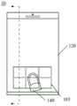
请参见图1至图4,电子设备10可以包括显示屏120和光学指纹识别模组130。Referring to FIGS. 1 to 4 , the
其中,显示屏120可以为自发光显示屏,其采用具有自发光的显示单元作为显示像素。比如显示屏120可以为有机发光二极管(Organic Light-Emitting Diode,OLED)显示屏或者微型发光二极管(Micro-LED)显示屏。在其他可替代实施例中,显示屏120也可以为液晶显示屏(Liquid Crystal Display, LCD)或者其他被动发光显示屏,本申请实施例对此不做限制。进一步地,显示屏120还可以具体为触控显示屏,其不仅可以进行画面显示,还可以检测用户的触摸或者按压操作,从而为用户提供一个人机交互界面。比如,在一种实施例中,电子设备10可以包括触摸传感器,所述触摸传感器可以具体为触控面板(Touch Panel,TP),其可以设置在所述显示屏120表面,也可以部分集成或者整体集成到所述显示屏120内部,从而形成所述触控显示屏。The
光学指纹模组130包括光学指纹传感器,所述光学指纹传感器包括具有多个光学感应单元131(也可以称为光学感应像素、感光像素、像素单元等) 的感应阵列133。所述感应阵列133所在区域或者其感应区域为所述光学指纹模组130的指纹检测区域103(也称为指纹采集区域、指纹识别区域等)。例如,所述光学感应单元131可以是光探测器,即所述感应阵列133具体可以为光探测器(Photo detector)阵列,其包括多个呈阵列式分布的光探测器。The
其中,所述光学指纹模组130设置在所述显示屏120下方的局部区域。Wherein, the
请继续参见图1,所述指纹检测区域103可以位于所述显示屏120的显示区域之中。在一种可替代实施例中,所述光学指纹模组130还可以设置在其他位置,比如所述显示屏120的侧面或者所述电子设备10的边缘非透光区域,并通过光路设计来将来自所述显示屏120的至少部分显示区域的光信号导引到所述光学指纹模组130,从而使得所述指纹检测区域103实际上位于所述显示屏120的显示区域。Please continue to refer to FIG. 1 , the
针对电子设备10,用户在需要对所述电子设备10进行解锁或者其他指纹验证的时候,只需要将手指按压在位于所述显示屏120的指纹检测区域 103,便可以实现指纹输入。由于指纹检测可以在屏内实现,因此采用上述结构的电子设备10无需其正面专门预留空间来设置指纹按键(比如Home键),从而可以采用全面屏方案,即所述显示屏120的显示区域可以基本扩展到整个电子设备10的正面。For the
请继续参见图2,所述光学指纹模组130可以包括光检测部分134和光学组件132。所述光检测部分134包括所述感应阵列133(也可称为光学指纹传感器)以及与所述感应阵列133电性连接的读取电路及其他辅助电路,其可以在通过半导体工艺制作在一个芯片(Die)上,比如光学成像芯片或者光学指纹传感器。所述光学组件132可以设置在所述光检测部分134的感应阵列133的上方,其可以具体包括滤光层(Filter)、导光层或光路引导结构、以及其他光学元件,所述滤光层可以用于滤除穿透手指的环境光,而所述导光层或光路引导结构主要用于从手指表面反射回来的反射光导引至所述感应阵列133进行光学检测。Please continue to refer to FIG. 2 , the
在本申请的一些实施例中,所述光学组件132可以与所述光检测部分134 封装在同一个光学指纹部件。比如所述光学组件132可以与所述光学检测部分134封装在同一个光学指纹芯片,也可以将所述光学组件132设置在所述光检测部分134所在的芯片外部,比如将所述光学组件132贴合在所述芯片上方,或者将所述光学组件132的部分元件集成在上述芯片之中。In some embodiments of the present application, the
在本申请的一些实施例中,所述光学指纹模组130的感应阵列133的所在区域或者光感应范围对应所述光学指纹模组130的指纹检测区域103。其中,所述光学指纹模组130的指纹采集区域103可以等于或不等于所述光学指纹模组130的感应阵列133的所在区域的面积或者光感应范围,本申请实施例对此不做具体限定。In some embodiments of the present application, the area or light sensing range of the
例如,通过光线准直方式进行光路引导,所述光学指纹模组130的指纹检测区域103可以设计成与所述光学指纹模组130的感应阵列的面积基本一致。For example, the optical path is guided by light collimation, and the
又例如,例如通过例如透镜成像的光路设计、反射式折叠光路设计或者其他光线会聚或者反射等光路设计,可以使得所述光学指纹模组130的指纹检测区域103的面积大于所述光学指纹模组130的感应阵列133的面积。For another example, the area of the
下面对光学组件132可以包括的光路引导结构进行示例性说明。The following is an exemplary description of the optical path guiding structure that the
以所述光路引导结构采用具有高深宽比的通孔阵列的光学准直器为例,所述光学准直器可以具体为在半导体硅片制作而成的准直器(Collimator)层,其具有多个准直单元或者微孔,所述准直单元可以具体为小孔,从手指反射回来的反射光中,垂直入射到所述准直单元的光线可以穿过并被其下方的传感器芯片接收,而入射角度过大的光线在所述准直单元内部经过多次反射被衰减掉,因此每一个传感器芯片基本只能接收到其正上方的指纹纹路反射回来的反射光,能够有效提高图像分辨率,进而提高指纹识别效果。Taking the optical path guiding structure using an optical collimator with a high aspect ratio through-hole array as an example, the optical collimator may be specifically a collimator layer fabricated on a semiconductor silicon wafer, which has A plurality of collimation units or micro-holes, the collimation unit can be specifically a small hole, from the reflected light from the finger, the light perpendicularly incident to the collimation unit can pass through and be received by the sensor chip below it , and the light with an excessively large incident angle is attenuated after multiple reflections inside the collimating unit, so each sensor chip can basically only receive the reflected light from the fingerprint pattern directly above it, which can effectively improve the image resolution. rate, thereby improving the fingerprint recognition effect.
以所述光路引导结构采用光学镜头的光路设计为例,所述光路引导结构可以为光学透镜(Lens)层,其具有一个或多个透镜单元,比如一个或多个非球面透镜组成的透镜组,其用于将从手指反射回来的反射光会聚到其下方的光检测部分134的感应阵列133,以使得所述感应阵列133可以基于所述反射光进行成像,从而得到所述手指的指纹图像。进一步地,所述光学透镜层在所述透镜单元的光路中还可以形成有针孔或者微孔光阑,比如,在所述透镜单元的光路中可以形成有一个或者多个遮光片,其中至少一个遮光片可以在所述透镜单元的光轴或者光学中心区域形成有透光微孔,所述透光微孔可以作为上述针孔或者微孔光阑。所述针孔或者微孔光阑可以配合所述光学透镜层和/或所述光学透镜层上方的其他光学膜层,扩大光学指纹模组130的视场,以提高所述光学指纹模组130的指纹成像效果。Taking the optical path design of the optical path guide structure using an optical lens as an example, the optical path guide structure can be an optical lens (Lens) layer, which has one or more lens units, such as a lens group composed of one or more aspherical lenses , which is used to condense the reflected light from the finger to the
以所述光路引导结构采用微透镜(Micro-Lens)层的光路设计为例,所述光路引导结构可以为包括由多个微透镜形成的微透镜阵列,其可以通过半导体生长工艺或者其他工艺形成在所述光检测部分134的感应阵列133上方,并且每一个微透镜可以分别对应于所述感应阵列133的其中一个感应单元。并且所述微透镜层和所述感应单元之间还可以形成其他光学膜层,比如介质层或者钝化层。更具体地,所述微透镜层和所述感应单元之间还可以包括具有微孔(或称为开孔)的挡光层(或称为遮光层、阻光层等),其中所述微孔形成在其对应的微透镜和感应单元之间,所述挡光层可以阻挡相邻微透镜和感应单元之间的光学干扰,并使得所述感应单元所对应的光线通过所述微透镜会聚到所述微孔内部并经由所述微孔传输到所述感应单元以进行光学指纹成像。Taking the optical path design of the optical path guiding structure using a micro-lens (Micro-Lens) layer as an example, the optical path guiding structure may include a microlens array formed by a plurality of microlenses, which may be formed by a semiconductor growth process or other processes Above the
应理解,上述针对光路引导结构的几种实现方案可以单独使用也可以结合使用。It should be understood that the above several implementation solutions for the optical path guiding structure can be used alone or in combination.
例如,可以在所述准直器层或者所述光学透镜层的上方或下方进一步设置微透镜层。当然,在所述准直器层或者所述光学透镜层与所述微透镜层结合使用时,其具体叠层结构或者光路可能需要按照实际需要进行调整。For example, a microlens layer may be further disposed above or below the collimator layer or the optical lens layer. Of course, when the collimator layer or the optical lens layer is used in combination with the microlens layer, its specific stack structure or optical path may need to be adjusted according to actual needs.
另一方面,所述光学组件132还可以包括其他光学元件,比如滤光层 (Filter)或其他光学膜片,其可以设置在所述光路引导结构和所述光学指纹传感器之间或者设置在所述显示屏120与所述光路引导结构之间,主要用于隔离外界干扰光对光学指纹检测的影响。其中,所述滤光层可以用于滤除穿透手指并经过所述显示屏120进入所述光学指纹传感器的环境光,与所述光路引导结构相类似,所述滤光层可以针对每个光学指纹传感器分别设置以滤除干扰光,或者也可以采用一个大面积的滤光层同时覆盖所述多个光学指纹传感器。On the other hand, the
指纹识别模组140可以用于采集用户的指纹信息(比如指纹图像信息)。The
以显示屏120采用具有自发光显示单元的显示屏为例,比如有机发光二极管(Organic Light-Emitting Diode,OLED)显示屏或者微型发光二极管 (Micro-LED)显示屏。所述光学指纹模组130可以利用所述OLED显示屏 120位于所述指纹检测区域103的显示单元(即OLED光源)作为光学指纹检测的激励光源。当手指140按压在所述指纹检测区域103时,显示屏120 向所述指纹检测区域103上方的目标手指140发出一束光111,该光111在手指140的表面发生反射形成反射光或者经过所述手指140内部散射而形成散射光(透射光)。在相关专利申请中,为便于描述,上述反射光和散射光统称为反射光。由于指纹的脊(ridge)141与谷(valley)142对于光的反射能力不同,因此,来自指纹脊的反射光151和来自指纹谷的反射光152具有不同的光强,反射光经过光学组件132后,被光学指纹模组130中的感应阵列133 所接收并转换为相应的电信号,即指纹检测信号;基于所述指纹检测信号便可以获得指纹图像数据,并且可以进一步进行指纹匹配验证,从而在电子设备10实现光学指纹识别功能。Taking the
在其他替代方案中,光学指纹模组130也可以采用内置光源或者外置光源来提供用于进行指纹检测识别的光信号。在这种情况下,光学指纹模组130 不仅可以适用于如OLED显示屏等自发光显示屏,还可以适用于非自发光显示屏,比如液晶显示屏或者其他的被动发光显示屏。In other alternative solutions, the
以应用在具有背光模组和液晶面板的液晶显示屏为例,为支持液晶显示屏的屏下指纹检测,电子设备10的光学指纹系统还可以包括用于光学指纹检测的激励光源,所述激励光源可以具体为红外光源或者特定波长非可见光的光源,其可以设置在所述液晶显示屏的背光模组下方或者设置在电子设备10 的保护盖板下方的边缘区域,而所述光学指纹模组130可以设置液晶面板或者保护盖板的边缘区域下方并通过光路引导以使得指纹检测光可以到达所述光学指纹模组130;或者,所述光学指纹模组130也可以设置在所述背光模组下方,且所述背光模组通过对扩散片、增亮片、反射片等膜层进行开孔或者其他光学设计以允许指纹检测光穿过液晶面板和背光模组并到达所述光学指纹模组130。当采用所述光学指纹模组130采用内置光源或者外置光源来提供用于进行指纹检测的光信号时,其检测原理与上面描述内容是一致的。Taking an application in a liquid crystal display with a backlight module and a liquid crystal panel as an example, in order to support fingerprint detection under the LCD screen, the optical fingerprint system of the
在具体实现上,所述电子设备10还可以包括透明保护盖板,所述盖板可以为玻璃盖板或者蓝宝石盖板,其位于所述显示屏120的上方并覆盖所述电子设备10的正面。因此,本申请实施例中,所谓的手指按压在所述显示屏 120实际上是指按压在所述显示屏120上方的盖板或者覆盖所述盖板的保护层表面。In terms of specific implementation, the
另一方面,所述光学指纹模组130可以仅包括一个光学指纹传感器,此时光学指纹模组130的指纹检测区域103的面积较小且位置固定,因此用户在进行指纹输入时需要将手指按压到所述指纹检测区域103的特定位置,否则光学指纹模组130可能无法采集到指纹图像而造成用户体验不佳。在其他替代实施例中,所述光学指纹模组130可以具体包括多个光学指纹传感器。所述多个光学指纹传感器可以通过拼接方式并排设置在所述显示屏120的下方,且所述多个光学指纹传感器的感应区域共同构成所述光学指纹模组130 的指纹检测区域103。从而所述光学指纹模组130的指纹检测区域103可以扩展到所述显示屏的下半部分的主要区域,即扩展到手指惯常按压区域,从而实现盲按式指纹输入操作。进一步地,当所述光学指纹传感器数量足够时,所述指纹检测区域103还可以扩展到半个显示区域甚至整个显示区域,从而实现半屏或者全屏指纹检测。On the other hand, the
请参见图3和图4,所述电子设备10中的光学指纹模组130可以包括多个光学指纹传感器,所述多个光学指纹传感器可以通过例如拼接等方式并排设置在所述显示屏120的下方,且所述多个光学指纹传感器的感应区域共同构成所述光学指纹装置130的指纹检测区域103。Referring to FIGS. 3 and 4 , the
进一步地,所述光学组件132可以包括多个光路引导结构,每个光路引导结构分别对应一个光学指纹传感器(即感应阵列133),并分别贴合设置在其对应的光学指纹传感器的上方。或者,所述多个光学指纹传感器也可以共享一个整体的光路引导结构,即所述光路引导结构具有一个足够大的面积以覆盖所述多个光学指纹传感器的感应阵列。Further, the
以所述光学组件132采用具有高深宽比的通孔阵列的光学准直器为例,所述当光学指纹模组130包括多个光学指纹传感器时,可以为每个光学指纹传感器的光学感应阵列中的一个光学感应单元配置一个或多个准直单元,并贴合设置在其对应的光学感应单元的上方。当然,所述多个光学感应单元也可以共享一个准直单元,即所述一个准直单元具有足够大的孔径以覆盖多个光学感应单元。由于一个准直单元可以对应多个光学感应单元或一个光学感应单元对应多个准直单元,破坏了显示屏120的空间周期和光学指纹传感器的空间周期的对应性,因此,即使显示屏120的发光显示阵列的空间结构和光学指纹传感器的光学感应阵列的空间结构类似,也能够有效避免光学指纹模组130利用经过显示屏120的光信号进行指纹成像生成莫尔条纹,有效提高了光学指纹模组130的指纹识别效果。Taking the
以所述光学组件132采用光学镜头为例,当光学指纹模组130包括多个传感器芯片时,可以为每一个传感器芯片配置一个光学镜头进行指纹成像,或者为多个传感器芯片配置一个光学镜头来实现光线会聚和指纹成像。甚至于,当一个传感器芯片具有两个感应阵列(Dual Array)或多个感应阵列 (Multi-Array)时,也可以为这个传感器芯片配置两个或多个光学镜头配合所述两个感应阵列或多个感应阵列进行光学成像,从而减小成像距离并增强成像效果。Taking the
应当理解,附图1至4仅为本申请的示例,不应理解为对本申请的限制。It should be understood that the accompanying
例如,本申请对指纹传感器的数量、尺寸和排布情况不做具体限定,其可以根据实际需求进行调整。例如,光学指纹模组130可以包括多个呈方形或圆形分布的多个指纹传感器。For example, the present application does not specifically limit the number, size and arrangement of fingerprint sensors, which can be adjusted according to actual needs. For example, the
需要说明的是,假设光学组件132包括的光学导引结构为光学准直器或微透镜阵列时,所述光学指纹模组130的感应阵列133的有效视受到到光学组件的面积的限制。以微透镜阵列为例,一般设计中,所述微透镜阵列位于感应阵列133的正上方或斜上方,且一个微透镜对应一个光学感应单元,即微透镜阵列中的每一个微透镜将接收到的光线聚焦至同一微透镜对应的光学感应单元。因此,所述感应阵列133的指纹识别区域受到微透镜阵列的尺寸的影响。It should be noted that, if the optical guiding structure included in the
因此,如何提升指纹识别的区域,成为一个亟待解决的技术问题。Therefore, how to improve the area of fingerprint identification has become an urgent technical problem to be solved.
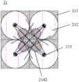
本申请实施例的指纹检测的装置适用于显示屏下方以实现屏下光学指纹检测。所述指纹检测装置可以适用于图1至图4所示的电子设备10,或者说所述装置可以是图1至图4所示的光学指纹模组130。如图5所示,所述指纹检测装置包括多个指纹检测单元21。The fingerprint detection device according to the embodiment of the present application is suitable for use under the display screen to realize off-screen optical fingerprint detection. The fingerprint detection apparatus may be applicable to the
应当理解,所述指纹检测装置可包括呈阵列分布或交错设置多个指纹检测单元,也可以包括呈中心对称或轴对称分布的多个指纹检测单元,本申请实施例对此不做具体限定。It should be understood that the fingerprint detection device may include a plurality of fingerprint detection units distributed in an array or staggered, and may also include a plurality of fingerprint detection units distributed centrally or axisymmetrically, which is not specifically limited in this embodiment of the present application.
其中,所述多个指纹检测单元中的每个指纹检测单元包括:多个光学感应像素、至少一个微透镜和至少一个挡光层。Wherein, each fingerprint detection unit in the plurality of fingerprint detection units includes: a plurality of optical sensing pixels, at least one microlens and at least one light blocking layer.
在具体实现中,所述至少一个微透镜可以设置在所述多个光学感应像素的上方;所述至少一个挡光层可设置在所述至少一个微透镜和所述多个光学感应像素之间,所述至少一层挡光层中每一层挡光层中设置有所述多个光学感应像素对应的开孔。其中,从所述显示屏上方的手指反射的多个方向上的倾斜光信号通过所述至少一个微透镜会聚后,通过所述至少一层挡光层中设置的开孔分别传输至所述多个光学感应像素,所述倾斜光信号用于检测所述手指的指纹信息。In a specific implementation, the at least one microlens may be disposed above the plurality of optical sensing pixels; the at least one light blocking layer may be disposed between the at least one microlens and the plurality of optical sensing pixels and each of the at least one light-blocking layer is provided with openings corresponding to the plurality of optical sensing pixels. Wherein, after the inclined light signals in multiple directions reflected from the finger above the display screen are collected by the at least one microlens, they are respectively transmitted to the multiple light-shielding layers through the openings provided in the at least one light-blocking layer. an optical sensing pixel, and the oblique light signal is used to detect the fingerprint information of the finger.
所述多个方向上的倾斜光信号可以是针对所述至少一个微透镜的倾斜光的入射方向。例如,可以将所述至少一个微透镜看作一个整体,此时在俯视图上,所述多个方向可以是所述至少一个微透镜接收到的来自上下左右4个方向的光信号,这4个方向的倾斜光信号相对所述显示屏所在的平面的夹角可以相同,也可以不同。所述多个方向可以是针对所述显示屏所在的平面而言的方向,也可以是针对立体空间而言的方向。所述多个方向可以互不相同,也可以部分不相同。The oblique light signals in the plurality of directions may be incident directions of oblique light for the at least one microlens. For example, the at least one microlens can be regarded as a whole. In this case, in a plan view, the multiple directions can be the light signals received by the at least one microlens from four directions: up, down, left, right, and four directions. The angle between the oblique optical signal in the direction and the plane on which the display screen is located may be the same or different. The multiple directions may be directions for a plane on which the display screen is located, or directions for a three-dimensional space. The multiple directions may be different from each other, and may also be partially different.
所述微透镜可以是各种具有会聚功能的镜头,用于增大视场,增加传输至感光像素的光信号量。所述微透镜的材料可以为有机材料,例如树脂。The microlenses can be various lenses with a converging function, which are used to increase the field of view and increase the amount of light signals transmitted to the photosensitive pixels. The material of the microlens may be an organic material, such as resin.
所述光学感应像素可以为光电传感器,用于将光信号转换为电信号。可选地,所述光学感应像素可以采用互补金属氧化物半导体(Complementary Metal OxideSemiconductor,CMOS)器件,由一个PN结组成的半导体器件,具有单方向导电特性。可选地,所述光学感应像素对于蓝光、绿光、红光或红外光的光灵敏度大于第一预定阈值,量子效率大于第二预定阈值。例如,该第一预定阈值可以为0.5v/lux-sec,该第二预定阈值可以为40%。也就是说,感光像素对于蓝光(波长为460±30nm)、绿光(波长为540±30nm)、红光或红外光(波长≥610nm)具有较高的光灵敏度和较高的量子效率,以便于检测相应的光。The optical sensing pixels may be photoelectric sensors for converting optical signals into electrical signals. Optionally, the optical sensing pixel may use a complementary metal oxide semiconductor (Complementary Metal Oxide Semiconductor, CMOS) device, which is a semiconductor device composed of a PN junction and has unidirectional conduction characteristics. Optionally, the optical sensitivity of the optical sensing pixel to blue light, green light, red light or infrared light is greater than a first predetermined threshold, and the quantum efficiency is greater than a second predetermined threshold. For example, the first predetermined threshold may be 0.5v/lux-sec, and the second predetermined threshold may be 40%. That is to say, the photosensitive pixel has high light sensitivity and high quantum efficiency for blue light (wavelength is 460±30nm), green light (wavelength is 540±30nm), red light or infrared light (wavelength ≥610nm), so that to detect the corresponding light.
应当理解,本申请实施例对所述微透镜和所述光学感应像素的具体形状不做限定。例如,所述多个光学感应像素中每个光学感应像素可以是四边形或六边形像素等多边形像素,也可以是其他形状像素,例如圆形像素,以使得所述多个光学感应像素具有更高的对称性,更高的采样效率,相邻像素等距,更好的角度分辨率,更少的混迭效应。It should be understood that the embodiments of the present application do not limit the specific shapes of the microlenses and the optical sensing pixels. For example, each optical sensing pixel in the plurality of optical sensing pixels may be a polygonal pixel such as a quadrilateral or hexagonal pixel, or may be a pixel of other shapes, such as a circular pixel, so that the plurality of optical sensing pixels have more High symmetry, higher sampling efficiency, equidistant adjacent pixels, better angular resolution, less aliasing effects.
还应理解,感光像素的上述参数可以对应于指纹检测所需的光,例如,若指纹检测所需的光仅为一种波段的光,则感光像素的上述参数仅需要满足该波段的光的要求即可。It should also be understood that the above parameters of the photosensitive pixel may correspond to the light required for fingerprint detection. For example, if the light required for fingerprint detection is only light of one wavelength band, the above parameters of the photosensitive pixel only need to satisfy the light of this wavelength band. on request.
在本申请实施例中,所述多个光学感应像素接收的信号为多个方向的倾斜光信号。即倾斜入射的多个方向的光信号。In the embodiment of the present application, the signals received by the plurality of optical sensing pixels are oblique optical signals in multiple directions. That is, optical signals in multiple directions of oblique incidence.
当干手指纹与OLED屏接触不好时,垂直方向的指纹图像的指纹脊和指纹谷的对比度差,图像模糊到分辨不了指纹纹路,本申请通过合理的光路设计,让光路接收倾斜光信号,在能够较好的获取正常手指指纹的同时,可以更好的检测出干手指指纹图像。在正常生活场景下,例如洗完手、早晨起床、手指抹灰、低温等场景下手指通常较干,其角质层不均匀,其按压在OLED 屏上时,手指局部区域会出现接触不良。这种情况的出现造成当前光学指纹方案对干手指纹识别的效果不好,本申请的有益效果就是提升干手指纹成像效果,让干手指纹图像变清晰。When the dry hand fingerprint is not in good contact with the OLED screen, the contrast between the fingerprint ridge and the fingerprint valley of the fingerprint image in the vertical direction is poor, and the image is blurred to the point where the fingerprint pattern cannot be distinguished. While the normal finger fingerprint can be better obtained, the dry finger fingerprint image can be better detected. In normal life scenarios, such as washing hands, getting up in the morning, plastering fingers, and low temperature, the fingers are usually dry, and the cuticle is uneven. When it is pressed on the OLED screen, the local area of the finger will have poor contact. The appearance of this situation causes the current optical fingerprint scheme to have a poor effect on the identification of dry hand fingerprints. The beneficial effect of the present application is to improve the imaging effect of the dry hand fingerprint, and make the dry hand fingerprint image clearer.
此外,通过所述至少一个微透镜对所述多个方向的倾斜光信号可以进行非正对光成像(即倾斜光成像),能够缩短所述光学感应像素阵列的光路设计 (即所述至少一个挡光层)的厚度,最终能够有效降低所述指纹检测装置的厚度。于此同时,通过对多个方向的倾斜光信号成像,能够扩大光学系统的物方数值孔径,进而提高指纹检测装置的鲁棒性以及公差容忍度。其中数值孔径可以用以衡量所述至少一个微透镜能够收集的光的角度范围。换言之,所述多个光学感应像素通过接收多个方向的光信号还能够扩大所述指纹检测单元的视场角和视场,进而增加所述指纹检测装置的视场角和视场,例如所述指纹检测装置的视场可以由6x9mm2扩展到7.5x10.5mm2,进一步提升指纹识别效果。In addition, the at least one microlens can perform non-positive light imaging (that is, oblique light imaging) on the oblique light signals in multiple directions, which can shorten the optical path design of the optical sensing pixel array (that is, the at least one The thickness of the light blocking layer) can finally effectively reduce the thickness of the fingerprint detection device. At the same time, by imaging oblique optical signals in multiple directions, the object-side numerical aperture of the optical system can be enlarged, thereby improving the robustness and tolerance tolerance of the fingerprint detection device. The numerical aperture can be used to measure the angular range of light that the at least one microlens can collect. In other words, the plurality of optical sensing pixels can also expand the field of view and field of view of the fingerprint detection unit by receiving light signals in multiple directions, thereby increasing the field of view and field of view of the fingerprint detection device. The field of view of the fingerprint detection device can be extended from 6x9mm2 to 7.5x10.5mm2 , which further improves the fingerprint recognition effect.
而且,通过在所述至少一个微透镜的下方设置多个光学感应像素,在所述至少一个微透镜的数量和所述多个光学感应像素的数量不相等时,可以使得微透镜的空间周期(即相邻微透镜之间的间距)和光学感应像素的空间周期(即相邻光学感应像素之间的间距)不相等,进而能够避免指纹图像中出现莫尔条纹并提升指纹识别效果。尤其是,所述至少一个微透镜的数量小于所述多个光学感应像素的数量时,可以减少透镜的成本以及提升所述多个光学感应像素的密度,进而降低所述指纹检测装置的尺寸和成本。Moreover, by arranging a plurality of optical sensing pixels under the at least one microlens, when the number of the at least one microlens is not equal to the number of the plurality of optical sensing pixels, the space period of the microlens ( That is, the spacing between adjacent microlenses) and the spatial period of the optical sensing pixels (ie the spacing between adjacent optical sensing pixels) are not equal, so that moire fringes can be avoided in fingerprint images and the fingerprint recognition effect can be improved. In particular, when the number of the at least one microlens is smaller than the number of the plurality of optical sensing pixels, the cost of the lens can be reduced and the density of the multiple optical sensing pixels can be increased, thereby reducing the size and size of the fingerprint detection device. cost.
与此同时,通过单个指纹检测单元可以复用多个角度的光信号(例如通过单个微透镜可以复用4个角度的光信号),可以对不同的物方孔径角的光束进行分割成像,有效提高了指纹检测装置的进光量,由此可以降低光学感应像素的曝光时长。At the same time, a single fingerprint detection unit can multiplex the optical signals of multiple angles (for example, the optical signals of 4 angles can be multiplexed through a single microlens). The light input amount of the fingerprint detection device is increased, thereby reducing the exposure time of the optical sensing pixels.
而且,由于所述多个光学感应像素分别能够接收到来自多个方向的倾斜光信号,因此按照倾斜光信号的方向,可以将所述多个光学感应像素划分为多个光学感应像素组,所述多个光学感应像素组可以分别用于接收所述多个方向的倾斜光信号,即每个光学感应像素组可以基于接收到的倾斜光信号生成一张指纹图像,由此所述多个光学感应像素组可以用于生成多张指纹图像,在这种情况下,可以将所述多张指纹图像进行叠加,以获取一张高分辨率的指纹图像,进而基于这张高分辨率的指纹图像进行指纹识别,可以提高指纹识别性能。Moreover, since the plurality of optical sensing pixels can respectively receive oblique light signals from multiple directions, the plurality of optical sensing pixels can be divided into multiple optical sensing pixel groups according to the directions of the oblique light signals, so The multiple optical sensing pixel groups can be respectively used to receive the oblique light signals in the multiple directions, that is, each optical sensing pixel group can generate a fingerprint image based on the received oblique optical signal, so that the multiple optical sensing pixel groups can generate a fingerprint image. The sensing pixel group can be used to generate multiple fingerprint images, in this case, the multiple fingerprint images can be superimposed to obtain a high-resolution fingerprint image, and then based on this high-resolution fingerprint image Performing fingerprint identification can improve the fingerprint identification performance.
基于以上分析可知,从所述显示屏上方的手指反射的多个方向上的倾斜光信号通过所述至少一个微透镜会聚后,通过所述至少一层挡光层中设置的开孔分别传输至所述多个光学感应像素,不仅能够降低所述多个光学感应像素的曝光时长,以及指纹检测装置的厚度和成本,而且能够提高指纹检测装置的鲁棒性、公差容忍度、视场角以及视场,进而提升指纹识别效果,尤其是干手指的指纹识别效果。Based on the above analysis, it can be seen that after the oblique light signals reflected from the finger above the display screen in multiple directions are condensed by the at least one microlens, they are respectively transmitted to the The multiple optical sensing pixels can not only reduce the exposure time of the multiple optical sensing pixels, as well as the thickness and cost of the fingerprint detection device, but also improve the robustness, tolerance tolerance, field of view and Field of view, thereby improving the fingerprint recognition effect, especially the fingerprint recognition effect of dry fingers.
下面结合附图对本申请实施例的指纹检测单元进行说明。The fingerprint detection unit of the embodiment of the present application will be described below with reference to the accompanying drawings.
在本申请的一些实施例中,所述至少一个微透镜的数量等于所述多个光学感应像素的数量,其中所述多个光学感应像素中的每一个光学感应像素的上方设置有一个微透镜。In some embodiments of the present application, the number of the at least one microlens is equal to the number of the plurality of optical sensing pixels, wherein a microlens is disposed above each optical sensing pixel of the plurality of optical sensing pixels .
例如,在一种实现方式中,所述至少一个微透镜为2x2微透镜矩形阵列,所述多个光学感应像素为2x2光学感应像素矩形阵列,所述2x2光学感应像素矩形阵列中的每一个光学感应像素的正上方设置有一个微透镜。For example, in an implementation manner, the at least one microlens is a 2x2 microlens rectangular array, the plurality of optical sensing pixels is a 2x2 optical sensing pixel rectangular array, and each optical sensing pixel in the 2x2 optical sensing pixel rectangular array is optically A microlens is arranged just above the sensing pixel.
又例如,在一种实现方式中,所述至少一个微透镜为2x2微透镜矩形阵列,所述多个光学感应像素为2x2光学感应像素矩形阵列,所述2x2光学感应像素矩形阵列中的每一个光学感应像素的斜上方设置有一个微透镜。For another example, in one implementation, the at least one microlens is a 2x2 microlens rectangular array, the plurality of optical sensing pixels is a 2x2 optical sensing pixel rectangular array, and each of the 2x2 optical sensing pixel rectangular arrays A micro-lens is arranged obliquely above the optical sensing pixel.
如图5所示,所述指纹检测单元21可包括呈矩形阵列分布的4个光学感应像素211和4个微透镜212,其中,每个光学感应像素211的正上方设置有一个微透镜212。As shown in FIG. 5 , the
此时,如图6所示,所述指纹检测单元21可包括顶层挡光层和底层挡光层。其中,所述顶层挡光层可包括分别对应所述4个微透镜212的4个开孔 2141,所述底层挡光层可包括分别对应所述4个微透镜212的4个开孔213。At this time, as shown in FIG. 6 , the
在一种实现中,所述2x2微透镜矩形阵列沿顺时针方向接收所述多个方向上的倾斜光信号,所述2x2微透镜矩形阵列中的每一个微透镜将接收到的倾斜光信号会聚至所述顺时针方向上的相邻微透镜下方的光学感应像素,或所述2x2微透镜矩形阵列沿逆时针方向接收所述多个方向上的倾斜光信号,所述2x2微透镜矩形阵列中的每一个微透镜将接收到的倾斜光信号会聚至所述逆时针方向上的相邻微透镜下方的光学感应像素。In one implementation, the 2x2 microlens rectangular array receives the oblique optical signals in the multiple directions in a clockwise direction, and each microlens in the 2x2 microlens rectangular array converges the received oblique optical signals to the optical sensing pixels below the adjacent microlenses in the clockwise direction, or the 2x2 microlens rectangular array receives the inclined light signals in the plurality of directions in the counterclockwise direction, in the 2x2 microlens rectangular array Each of the microlenses converges the received oblique light signal to the optical sensing pixel below the adjacent microlens in the counterclockwise direction.
例如,如图7所示,所述4个微透镜212可以沿以下路径将多个方向的倾斜光信号分别会聚至所述4个光学感应像素211:For example, as shown in FIG. 7 , the four
右上角的微透镜212将接收到的倾斜光信号会聚至左上角的光学感应像素211,左上角的微透镜212将接收到的倾斜光信号会聚至左下角的光学感应像素211,左下角的微透镜212将接收到的倾斜光信号会聚至右下角的光学感应像素211,以及右下角的微透镜212将接收到的倾斜光信号会聚至右上角的光学感应像素211。The
由此,所述指纹检测装置包括阵列分布的多个指纹检测单元时,可以基于接收到的多个方向的光信号生成多幅指纹图像,进而得到一幅高分辨率的指纹图像,以提升指纹识别效果。Therefore, when the fingerprint detection device includes multiple fingerprint detection units distributed in an array, multiple fingerprint images can be generated based on the received optical signals in multiple directions, and then a high-resolution fingerprint image can be obtained, so as to improve the fingerprint quality. Identify the effect.
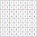
例如,所述4x4指纹检测单元矩形阵列可以包括如图8所示的光学感应像素阵列,其中,“1”表示用于接收第一方向的倾斜光信号的光学感应像素,“2”表示用于接收第二方向的倾斜光信号的光学感应像素,“3”表示用于接收第三方向的倾斜光信号的光学感应像素,“4”表示用于接收第四方向的倾斜光信号的光学感应像素。也就是说,“1”、“2”、“3”以及“4”表示的光学感应像素分别可以用于生成一幅指纹图像,即总共可以生成4幅指纹图像,这4幅指纹图像可以用于合并成一幅高分辨率的指纹图像,进而提升指纹检测装置的识别效果。For example, the 4×4 fingerprint detection unit rectangular array may include an optical sensing pixel array as shown in FIG. 8 , wherein “1” represents an optical sensing pixel for receiving an oblique light signal in the first direction, and “2” represents an optical sensing pixel used for receiving the oblique light signal in the first direction. The optical sensing pixel that receives the oblique light signal in the second direction, "3" represents the optical sensing pixel for receiving the oblique light signal in the third direction, and "4" represents the optical sensing pixel for receiving the oblique light signal in the fourth direction . That is to say, the optical sensing pixels represented by "1", "2", "3" and "4" can be used to generate a fingerprint image respectively, that is, a total of 4 fingerprint images can be generated, and these 4 fingerprint images can be used It can be combined into a high-resolution fingerprint image, thereby improving the recognition effect of the fingerprint detection device.
结合图7来说,所述第一方向可以是针对右下角微透镜212接收的倾斜光信号所在的方向,所述第二方向可以是针对右上角微透镜212接收的倾斜光信号所在的方向,所述第三方向可以是针对左上角微透镜212接收的倾斜光信号所在的方向,所述第四方向可以是针对左下角微透镜212接收的倾斜光信号所在的方向。Referring to FIG. 7 , the first direction may be the direction in which the oblique optical signal received by the
图9是位于显示屏下方的指纹检测装置的侧视图。FIG. 9 is a side view of the fingerprint detection device under the display screen.
如图9所示,所述指纹检测装置可包括呈阵列分布的微透镜212,位于微透镜212下方的顶层挡光层和底层挡光层,以及位于底层挡光层下方的呈阵列分布的光学感应像素,其中针对每个微透镜212,所述顶层挡光层和底层挡光层分别形成有对应的开孔2141和开孔213。所述指纹检测装置设置在显示屏216的下方。As shown in FIG. 9 , the fingerprint detection device may include
其中,每个微透镜212通过对应的开孔2141以及开孔213将接收到的具有特定方向的倾斜光信号(图中实线所示的光信号)会聚至对应的光学感应像素,并将接收到的非特定方向的倾斜光信号(图中虚线所示的光信号)传输至挡光层中除开孔2141以及开孔214之外的区域,以避免被其他光学感应像素接收,进而实现指纹图像的分割成像。Wherein, each
图10是本申请实施例针对两个方向倾斜光信号的光路示意图。FIG. 10 is a schematic diagram of an optical path of an optical signal inclined in two directions according to an embodiment of the present application.
结合图7来说,图10可以是包括图7所示的指纹检测单元的指纹检测装置在A-A'方向上的示意性侧剖面图,此时,指纹检测单元中的一个微透镜212 (例如图7所示的右上角微透镜212)通过对应的开孔2141以及开孔213将接收到的一个方向(即所述第二方向)的倾斜光信号(图10中实线所示的光信号)会聚至对应的光学感应像素(例如图7所示的左上角光学感应像素 211),指纹检测单元中的另一微透镜212(例如图7所示的左下角微透镜212)通过对应的开孔2141以及开孔213将接收到的另一方向(即所述第四方向) 的倾斜光信号(图10中虚线所示的光信号)会聚至对应的光学感应像素(例如图7所示的右下角光学感应像素211)。7, FIG. 10 may be a schematic side sectional view of the fingerprint detection device including the fingerprint detection unit shown in For example, the upper
例如,如图10所示,包括多个指纹检测单元的指纹检测装置的指纹识别区域包括第一指纹识别区域和第二指纹识别区域,其中用于汇聚所述第二方向上的倾斜光信号的微透镜212对应的指纹识别区域为第一指纹识别区域,用于会聚所述第四方向上的倾斜光信号的微透镜对应的指纹识别区域为第二指纹识别区域。所述第一指纹识别区域相对光学感应像素形成的阵列向右偏移第一增加区域,所述第二指纹识别区域相对光学感应像素形成的这列向左偏移第二增加区域。For example, as shown in FIG. 10 , the fingerprint identification area of the fingerprint detection device including a plurality of fingerprint detection units includes a first fingerprint identification area and a second fingerprint identification area, wherein the The fingerprint recognition area corresponding to the
换言之,相对仅接收一个方向的倾斜光信号的指纹检测装置,本申请实施例提供的指纹检测装置的指纹识别区域额外包括所述第一增加区域和所述第二增加区域,有效增加了可视区域(即视场)。此外,所述第一指纹识别区域和所述第二指纹识别区域的重叠区域,能够有效提高指纹图像的图像分辨率,进而提升了指纹识别效果。In other words, compared with a fingerprint detection device that only receives an oblique light signal in one direction, the fingerprint recognition area of the fingerprint detection device provided by the embodiment of the present application additionally includes the first increased area and the second increased area, effectively increasing the visibility area (ie field of view). In addition, the overlapping area of the first fingerprint identification area and the second fingerprint identification area can effectively improve the image resolution of the fingerprint image, thereby improving the fingerprint identification effect.
应理解,图7所示的光路设计仅为本申请的示例,不应理解为对本申请的限制。It should be understood that the optical path design shown in FIG. 7 is only an example of the present application, and should not be construed as a limitation of the present application.
在另一种实现中,所述2x2微透镜矩形阵列沿所述2x2微透镜矩形阵列的对角线方向接收所述多个方向上的倾斜光信号,所述2x2微透镜矩形阵列中每一个微透镜将接收到的倾斜光信号会聚至所述对角线方向上的相邻微透镜下方的光学感应像素。In another implementation, the 2x2 microlens rectangular array receives the slanted optical signals in the plurality of directions along a diagonal direction of the 2x2 microlens rectangular array, and each microlens in the 2x2 microlens rectangular array receives The lens converges the received oblique light signal to the optical sensing pixels below the adjacent microlenses in the diagonal direction.
例如,如图11和图12所示,所述4个微透镜212可以沿以下路径将多个方向的倾斜光信号分别会聚至所述4个光学感应像素211:For example, as shown in FIG. 11 and FIG. 12 , the four
右上角的微透镜212将接收到的倾斜光信号会聚至左下角的光学感应像素211,左下角的微透镜212将接收到的倾斜光信号会聚至右上角的光学感应像素211,左上角的微透镜212将接收到的倾斜光信号会聚至右下角的光学感应像素211,以及右下角的微透镜212将接收到的倾斜光信号会聚至左上角的光学感应像素211。The
由此,所述指纹检测装置包括阵列分布的多个指纹检测单元时,可以基于接收到的多个方向的光信号生成多幅指纹图像,进而得到一幅高分辨率的指纹图像,以提升指纹识别效果。Therefore, when the fingerprint detection device includes multiple fingerprint detection units distributed in an array, multiple fingerprint images can be generated based on the received optical signals in multiple directions, and then a high-resolution fingerprint image can be obtained, so as to improve the fingerprint quality. Identify the effect.
类似地,所述4x4指纹检测单元矩形阵列可以包括如图8所示的光学感应像素阵列,其中,“1”表示用于接收第一方向的倾斜光信号的光学感应像素,“2”表示用于接收第二方向的倾斜光信号的光学感应像素,“3”表示用于接收第三方向的倾斜光信号的光学感应像素,“4”表示用于接收第四方向的倾斜光信号的光学感应像素。也就是说,“1”、“2”、“3”以及“4”表示的光学感应像素分别可以用于生成一幅指纹图像,即总共可以生成4幅指纹图像,这4幅指纹图像可以用于合并成一幅高分辨率的指纹图像,进而提升指纹检测装置的识别效果。Similarly, the 4×4 fingerprint detection unit rectangular array may include an optical sensing pixel array as shown in FIG. 8 , wherein “1” represents an optical sensing pixel for receiving an oblique light signal in the first direction, and “2” represents an optical sensing pixel with For the optical sensing pixel receiving the oblique light signal in the second direction, "3" represents the optical sensing pixel for receiving the oblique optical signal in the third direction, and "4" represents the optical sensing pixel for receiving the oblique optical signal in the fourth direction. pixel. That is to say, the optical sensing pixels represented by "1", "2", "3" and "4" can be used to generate a fingerprint image respectively, that is, a total of 4 fingerprint images can be generated, and these 4 fingerprint images can be used It can be combined into a high-resolution fingerprint image, thereby improving the recognition effect of the fingerprint detection device.
结合图11来说,所述第一方向可以是针对左下角微透镜212接收的倾斜光信号所在的方向,所述第二方向可以是针对右下角微透镜212接收的倾斜光信号所在的方向,所述第三方向可以是针对右上角微透镜212接收的倾斜光信号所在的方向,所述第四方向可以是针对左上角微透镜212接收的倾斜光信号所在的方向。Referring to FIG. 11 , the first direction may be the direction in which the oblique light signal received by the lower
应理解,本申请实施例中,所述指纹检测单元包括至少一个挡光层和多个光学感应像素,其中所述至少一层挡光层中每一层挡光层中设置有所述多个光学感应像素对应的开孔。例如,所述至少一层挡光层可为多层挡光层,所述多层挡光层的顶层挡光层可设置有所述多个光学感应像素对应的至少一个开孔。例如,所述多层挡光层的顶层挡光层可设置有所述多个光学感应像素对应的一个开孔。又例如,所述多层挡光层的顶层挡光层可设置有所述多个光学感应像素分别对应的多个开孔It should be understood that, in this embodiment of the present application, the fingerprint detection unit includes at least one light blocking layer and a plurality of optical sensing pixels, wherein each of the at least one light blocking layer is provided with the plurality of light blocking layers. The openings corresponding to the optical sensing pixels. For example, the at least one light-blocking layer may be a multi-layer light-blocking layer, and the top light-blocking layer of the multilayer light-blocking layer may be provided with at least one opening corresponding to the plurality of optical sensing pixels. For example, the top light-blocking layer of the multilayer light-blocking layer may be provided with an opening corresponding to the plurality of optical sensing pixels. For another example, the top light-blocking layer of the multilayer light-blocking layer may be provided with a plurality of openings corresponding to the plurality of optical sensing pixels respectively
例如,如图12所示,所述至少一层挡光层可包括顶层挡光层和底层挡光层,其中所述顶层挡光层设置有4个光学感应像素分别对应的4个开孔2141。底层挡光层设置有4个光学感应像素分别对应的4个开孔213。For example, as shown in FIG. 12 , the at least one light-blocking layer may include a top light-blocking layer and a bottom light-blocking layer, wherein the top light-blocking layer is provided with four
例如,如图13所示,所述至少一层挡光层可包括顶层挡光层和底层挡光层,其中所述顶层挡光层设置有4个光学感应像素对应的1个开孔2142。底层挡光层设置有4个光学感应像素分别对应的4个开孔213。For example, as shown in FIG. 13 , the at least one light-blocking layer may include a top light-blocking layer and a bottom light-blocking layer, wherein the top light-blocking layer is provided with one
应理解,图12和图13中挡光层中设置的开孔仅以图11所示的指纹检测单元为例进行了说明,其实现方式可适用于本申请的各种实施例,本申请对此不做限制。It should be understood that the openings provided in the light-blocking layer in FIG. 12 and FIG. 13 are only described by taking the fingerprint detection unit shown in FIG. 11 as an example, and its implementation can be applied to various embodiments of the present application. This does not limit.
例如,所述至少一个挡光层可以是大于2层的挡光层。For example, the at least one light blocking layer may be more than 2 light blocking layers.
还应理解,图5至图13仅为每一个光学感应像素的上方设置有一个微透镜的示例,不应理解为对本申请的限制。例如,例如,所述指纹检测单元还可包括其它数量或其它排列方式的微透镜或光学感应像素。It should also be understood that FIG. 5 to FIG. 13 are only examples in which a microlens is disposed above each optical sensing pixel, and should not be construed as a limitation of the present application. For example, the fingerprint detection unit may further include other numbers or other arrangements of microlenses or optical sensing pixels.
例如,在另一种实现方式中,所述至少一个微透镜为多排微透镜,所述多个光学感应像素为所述多排微透镜对应的多排光学感应像素,其中所述多排光学感应像素中的每一排光学感应像素错位设置在对应的一排微透镜的下方。For example, in another implementation manner, the at least one microlens is multiple rows of microlenses, and the multiple optical sensing pixels are multiple rows of optical sensing pixels corresponding to the multiple rows of microlenses, wherein the multiple rows of optical sensing pixels are multiple rows of optical sensing pixels corresponding to the multiple rows of microlenses. Each row of optical sensing pixels in the sensing pixels is disposed under a corresponding row of microlenses by dislocation.
可选地,所述多排微透镜可以是多列或多行微透镜。Optionally, the multiple rows of microlenses may be multiple columns or rows of microlenses.
其中,所述至少一层挡光层可设置有相应的光路设计,以使得所述多排微透镜沿所述多排光学感应像素的错位方向接收所述多个方向上的倾斜光信号,所述多排微透镜中的每一排微透镜将接收到的倾斜光信号汇聚至同一排微透镜或相邻微透镜下的光学感应像素。Wherein, the at least one light-blocking layer may be provided with a corresponding optical path design, so that the multiple rows of microlenses receive the inclined light signals in the multiple directions along the misalignment direction of the multiple rows of optical sensing pixels, so Each row of microlenses in the plurality of rows of microlenses converges the received oblique light signal to the optical sensing pixels under the same row of microlenses or adjacent microlenses.
例如,如图14所示,所述指纹检测单元22可包括呈矩形阵列分布的4 列光学感应像素和所述4列光学感应像素对应的4列微透镜,其中这4列光学感应像素中的每列光学感应像素包括6个光学感应像素221,这4列微透镜中的每列微透镜包括6个微透镜222,一个光学感应像素221错位设置在一个微透镜222的下方。For example, as shown in FIG. 14 , the
例如,所述指纹检测单元22可包括顶层挡光层和底层挡光层。此时,针对每个微透镜222,所述顶层挡光层和所述底层挡光层可分别设置有其对应的开孔2241和开孔2231。其中,所述多排微透镜中的每一排微透镜中的每一个微透镜222通过对应的开孔2241和开孔2231可以将接收到的光信号会聚至同一微透镜222斜下方的光学感应像素221。For example, the
由此,所述指纹检测装置包括阵列分布的多个指纹检测单元时,可以基于接收到的多个方向的光信号生成多幅指纹图像,进而得到一幅高分辨率的指纹图像,以提升指纹识别效果。Therefore, when the fingerprint detection device includes multiple fingerprint detection units distributed in an array, multiple fingerprint images can be generated based on the received optical signals in multiple directions, and then a high-resolution fingerprint image can be obtained, so as to improve the fingerprint quality. Identify the effect.
例如,图14所示的指纹检测单元可以包括如图15所示的光学感应像素阵列,其中,“1”表示用于接收第一方向的倾斜光信号的光学感应像素,“2”表示用于接收第二方向的倾斜光信号的光学感应像素。也就是说,“1”和“2”、表示的光学感应像素分别可以用于生成一幅指纹图像,即总共可以生成2幅指纹图像,这2幅指纹图像可以用于合并成一幅高分辨率的指纹图像,进而提升指纹检测装置的识别效果。For example, the fingerprint detection unit shown in FIG. 14 may include an optical sensing pixel array as shown in FIG. 15 , wherein “1” represents the optical sensing pixel for receiving the oblique light signal in the first direction, and “2” represents the optical sensing pixel for receiving the oblique light signal in the first direction. An optical sensing pixel that receives the oblique light signal in the second direction. That is to say, the optical sensing pixels represented by "1" and "2" can be used to generate a fingerprint image respectively, that is, a total of 2 fingerprint images can be generated, and these 2 fingerprint images can be combined into a high-resolution image The fingerprint image is obtained, thereby improving the recognition effect of the fingerprint detection device.
结合图14来说,基于由左向右的顺序,所述第一方向可以是针对第一列和第二列微透镜中的微透镜接收的倾斜光信号所在的方向,所述第二方向可以是第三列和第四列微透镜接收的倾斜光信号所在的方向。Referring to FIG. 14 , based on the order from left to right, the first direction may be the direction in which the oblique light signals received by the microlenses in the first column and the second column of microlenses are located, and the second direction may be is the direction of the oblique light signal received by the third and fourth columns of microlenses.
可选地,在本申请的一个实施例中,所述多排微透镜中的每一排微透镜中的每一个微透镜在所述显示屏所在平面的投影为圆形,所述多排光学感应像素中的每一排光学感应像素中的每一个光学感应像素在所述显示屏所在平面的投影为矩形,所述多排光学感应像素中的每一排光学感应像素中的每一个光学感应像素的中心在所述显示屏所在的平面上的投影,相对对应的微透镜的中心在所述显示屏所在的平面上的投影,沿所述多排光学感应像素的错位方向偏移预设距离,所述预设距离小于或等于所述矩形的边长,或所述预设距离小于或等于所述圆形的直径。Optionally, in an embodiment of the present application, the projection of each microlens in each row of microlenses in the multi-row microlenses on the plane where the display screen is located is a circle, and the multi-row optical lens The projection of each optical sensing pixel in each row of optical sensing pixels in the sensing pixels on the plane where the display screen is located is a rectangle, and each optical sensing pixel in each row of optical sensing pixels in the multiple rows of optical sensing pixels The projection of the center of the pixel on the plane where the display screen is located, relative to the projection of the center of the corresponding microlens on the plane where the display screen is located, is offset by a preset distance along the misalignment direction of the multiple rows of optical sensing pixels , the preset distance is less than or equal to the side length of the rectangle, or the preset distance is less than or equal to the diameter of the circle.
例如,如图14所示,所述错位方向为所述多排光学感应像素中的每一排光学感应像素中的每一个光学感应像素的对角线方向,即所述多排光学感应像素中的每一排光学感应像素中的每一个光学感应像素221沿同一光学感应像素221的对角线方向偏移预设距离。For example, as shown in FIG. 14 , the dislocation direction is the diagonal direction of each optical sensing pixel in each row of optical sensing pixels in the multiple rows of optical sensing pixels, that is, in the multiple rows of optical sensing pixels Each
此时,所述多排光学感应像素中的每一排光学感应像素中的每一个光学感应像素221的上方可设置有其对应的开孔2241和开孔2231,即所述指纹检测单元22中的至少一层挡光层在每一个光学感应像素221的上方设置有其对应的开孔。At this time, a
应当理解,所述预设距离也可以是在光学感应像素221的边长所在的方向的偏移距离,例如,以光学感应像素221的两个边长为X轴方向和Y轴方向,其中,所述预设距离可以包括沿X轴方向的偏移距离和沿Y轴方向的偏移距离。例如,假设所述光学感应像素的边长为12.5mm,所述微透镜的直径为11.5mm,沿X轴方向的偏移距离可以为4~5mm,沿Y轴方向的偏移距离可以为4~5mm。当然,上述参数仅为示例,不应理解为对本身的限制,例如,所述沿X轴方向的偏移距离也可以不等于沿Y轴方向的偏移距离,又例如,所述沿X轴方向的偏移距离或所述沿Y轴方向的偏移距离可以是大于5mm 或小于4mm。It should be understood that the preset distance may also be an offset distance in the direction in which the side length of the
当然,图14仅为本申请实施例中多排光学感应像素偏移的示例,不应理解为对本申请的限制。Of course, FIG. 14 is only an example of the offset of multiple rows of optical sensing pixels in the embodiment of the present application, and should not be construed as a limitation on the present application.
例如,如图16所示,所述错位方向为所述多排光学感应像素中的每一排光学感应像素中的每一个光学感应像素的竖直边长所在的方向。所述竖直边长可以是与光学感应像素的排列方向平行的方向。For example, as shown in FIG. 16 , the dislocation direction is the direction in which the vertical side length of each optical sensing pixel in each row of optical sensing pixels in the multiple rows of optical sensing pixels is located. The vertical side length may be a direction parallel to the arrangement direction of the optical sensing pixels.
例如,所述指纹检测单元22可包括顶层挡光层和底层挡光层。此时,针对每个微透镜222,所述顶层挡光层和所述底层挡光层可分别设置有其对应的开孔2242和开孔2232。其中,所述多排微透镜中的每一排微透镜中的每一个微透镜222通过对应的开孔2242和开孔2232可以将接收到的倾斜光信号会聚至相邻微透镜222正下方的光学感应像素221。例如,左上角微透镜 222可将接收到的倾斜光信号会聚至相邻的第二行第一列微透镜222正下方的光学感应像素221。For example, the
此时,所述底层挡光层可在所述多排光学感应像素中的每一排光学感应像素中的每一个光学感应像素221的上方设置其对应的开孔2232,以及所述顶层挡光层可在与同一光学感应像素221相邻的光学感应像素221的上方设置有其对应的开孔2242。At this time, the bottom light blocking layer can be provided with a
当然,在其他可替代实施例中,所述错位方向也可以为其他方向,例如,所述错位方向为所述多排光学感应像素中的每一排光学感应像素中的每一个光学感应像素的水平边长所在的方向。所述水平边长可以是与光学感应像素的排列方向垂直的方向。Of course, in other alternative embodiments, the misalignment direction may also be other directions, for example, the misalignment direction is the direction of each optical sensing pixel in each row of optical sensing pixels in the multiple rows of optical sensing pixels The direction of the horizontal side length. The horizontal side length may be a direction perpendicular to the arrangement direction of the optical sensing pixels.
在本申请的另一些实施例中,所述至少一个微透镜的数量小于所述多个光学感应像素的数量。In other embodiments of the present application, the number of the at least one microlens is smaller than the number of the plurality of optical sensing pixels.
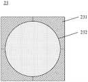
在一种实现方式中,所述至少一个微透镜为一个微透镜,所述多个光学感应像素为2x2光学感应像素矩形阵列,其中所述一个微透镜设置在所述2x2 光学感应像素矩形阵列的正上方。In an implementation manner, the at least one microlens is a microlens, the plurality of optical sensing pixels are a 2×2 rectangular array of optical sensing pixels, wherein the one microlens is disposed in the rectangular array of 2×2 optical sensing pixels Directly above.
例如,如图17所示,所述指纹检测装置23可包括一个微透镜232和呈矩形阵列分布的4个光学感应像素231。For example, as shown in FIG. 17 , the
在具体实现中,所述指纹检测装置23中的至少一个挡光层可在所述一个微透镜的下方分别设置有所述4个光学感应像素231对应的开孔,以使得所述一个微透镜可沿所述2x2光学感应像素矩形阵列的对角线方向接收所述多个方向上的倾斜光信号,所述一个微透镜将所述多个方向上的倾斜光信号可沿所述对角线方向分别会聚至所述2x2光学感应像素矩形阵列中的光学感应像素,以增加每个光学感应像素能够接收到的信号量,进而提升指纹识别效果。In a specific implementation, at least one light-blocking layer in the
例如,如图18和图19所示,所述至少一个挡光层可包括顶层挡光层和底层挡光层。所述顶层挡光层在所述一个微透镜232的下方设置有所述4个光学感应像素231分别对应的开孔2341,所述底层挡光层在所述一个微透镜 232的下方设置有所述4个光学感应像素231分别对应的开孔232。所述一个微透镜232通过对应的开孔2341以及开孔232将接收到的多个方向的光信号分别会聚至所述4个光学感应像素231。For example, as shown in FIGS. 18 and 19 , the at least one light blocking layer may include a top light blocking layer and a bottom light blocking layer. The top light-blocking layer is provided with
当然,所述顶层挡光层的对应所述4个光学感应像素231的4个小孔也可以合并为一个大孔。例如图20和图21所示的开孔2342。Of course, the four small holes of the top light blocking layer corresponding to the four
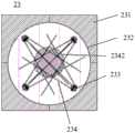
在另一种实现方式中,所述一个微透镜为2x2微透镜矩形阵列,所述多个光学感应像素为3x3光学感应像素矩形阵列,所述3x3矩形阵列中每相邻的4个光学感应像素的正上方设置有一个微透镜。例如,所述3x3矩形阵列中每相邻的4个光学感应像素的中心位置的正上方设置有一个微透镜。In another implementation manner, the one microlens is a 2×2 microlens rectangular array, the plurality of optical sensing pixels is a 3×3 optical sensing pixel rectangular array, and each adjacent 4 optical sensing pixels in the 3×3 rectangular array There is a microlens directly above it. For example, in the 3×3 rectangular array, a microlens is disposed just above the center position of each of the four adjacent optical sensing pixels.
例如,如图22所示,所述指纹检测装置24可包括呈矩形阵列分布的4 个微透镜242和呈矩形阵列分布的9个光学感应像素241。For example, as shown in FIG. 22 , the
在具体实现中,所述指纹检测装置24中的至少一个挡光层可分别设置有所述3x3光学感应像素矩形阵列的4个角上的光学感应像素241对应的开孔,以使得所述2x2微透镜矩形阵列中的每一个微透镜242可将接收到的倾斜光信号会聚至所述3x3光学感应像素矩形阵列的4个角上的光学感应像素241 中的距离同一微透镜424距离最近的光学感应像素241。In a specific implementation, at least one light-blocking layer in the
例如,如图23所示,所述至少一个挡光层可包括顶层挡光层和底层挡光层。所述顶层挡光层设置有所述4个角上的光学感应像素241分别对应的开孔244,所述底层挡光层设置有所述4个角上的光学感应像素241分别对应的开孔243。由此,所述4个微透镜242可通过对应的开孔2341和开孔243 将所述多个方向的倾斜光信号分别会聚至所述4个角上的光学感应像素241。For example, as shown in FIG. 23 , the at least one light blocking layer may include a top light blocking layer and a bottom light blocking layer. The top light blocking layer is provided with
由于所述3x3光学感应像素矩形阵列中只有4个角上的光学感应像素241 会接收到用于检测指纹信息的倾斜光信号,因此,为了增加光学感应像素的利用率,在本申请的一些实施例中,可以通过交错排列的方式可形成包括多个指纹检测单元24的指纹检测装置。Since only the
例如,如图24所示,位于中间位置的中心指纹检测单元,其左上角光学感应像素241和右上角光学感应像素241之间的光学感应像素241可被复用为另一个指纹检测单元的位于左下角的光学感应像素241,所述中心指纹检测单元的左上角光学感应像素241和左下角光学感应像素241之间的光学感应像素241可被复用为另一指纹检测单元的位于右下角的光学感应像素241,所述中心指纹检测单元的左下角光学感应像素241和右下角光学感应像素 241之间的光学感应像素241可被复用于另一指纹检测单元的位于右上角的光学感应像素241,所述中心指纹检测单元的右下角光学感应像素241和右上角光学感应像素241之间的光学感应像素241可被复用于另一指纹检测单元的位于左上角的光学感应像素241。For example, as shown in FIG. 24 , the
由此,所述指纹检测装置可包括如图25所示的多个光学感应像素,其中,“0”表示不用于接收光信号的光学感应像素,“1”、“2”、“3”以及“4”分别表示用于接收4个不同方向的光学感应像素。也就是说,“1”、“2”、“3”以及“4”表示的光学感应像素分别可以用于生成一幅指纹图像,即总共可以生成4幅指纹图像,这4幅指纹图像可以用于合并成一幅高分辨率的指纹图像,进而提升指纹检测装置的识别效果。Thus, the fingerprint detection device may include a plurality of optical sensing pixels as shown in FIG. 25 , wherein “0” represents an optical sensing pixel not used for receiving optical signals, “1”, “2”, “3” and "4" respectively represent optical sensing pixels for receiving 4 different directions. That is to say, the optical sensing pixels represented by "1", "2", "3" and "4" can be used to generate a fingerprint image respectively, that is, a total of 4 fingerprint images can be generated, and these 4 fingerprint images can be used It can be combined into a high-resolution fingerprint image, thereby improving the recognition effect of the fingerprint detection device.
在另一种实现方式中,所述至少一个微透镜为3x3微透镜矩形阵列,所述多个光学感应像素为4x4光学感应像素矩形阵列,所述4x4光学感应像素矩形阵列中每相邻的4个光学感应像素的正上方设置有一个微透镜。In another implementation manner, the at least one microlens is a 3×3 microlens rectangular array, the plurality of optical sensing pixels is a 4×4 optical sensing pixel rectangular array, and each adjacent 4 optical sensing pixels in the 4×4 optical sensing pixel rectangular array A microlens is arranged directly above each optical sensing pixel.
例如,如图26所示,所述指纹检测装置24可包括呈矩形阵列分布的9 个微透镜252和呈矩形阵列分布的16个光学感应像素251。其中,所述16 个光学感应像素251中每相邻的4个光学感应像素251的正上方设置有一个微透镜252。For example, as shown in FIG. 26 , the
在具体实现中,所述指纹检测装置24中的至少一个挡光层可分别设置有所述16个的光学感应像素251对应的开孔,以使得所述3x3微透镜矩形阵列中的中心微透镜将接收到的倾斜光信号分别会聚至所述中心微透镜下方的4 个光学感应像素,所述3x3微透镜矩形阵列中的4个角上的微透镜中的每一个微透镜将接收到的倾斜光信号会聚至同一微透镜下方的位于所述4x4光学感应像素矩形阵列的角上的光学感应像素,所述3x3微透镜矩形阵列中的其他微透镜中的每一个微透镜将接收到的倾斜光信号会聚至同一微透镜下方的外侧的两个光学感应像素。In a specific implementation, at least one light-blocking layer in the
例如,如图27所示,所述至少一个挡光层可包括顶层挡光层和底层挡光层。所述顶层挡光层设置有所述16个的光学感应像素251分别对应的开孔 2541,所述底层挡光层设置有所述16个的光学感应像素251分别对应的开孔 253。由此,所述9个微透镜252可通过对应的开孔2341和开孔243将所述多个方向的倾斜光信号分别会聚至所述16个光学感应像素251。For example, as shown in FIG. 27 , the at least one light blocking layer may include a top light blocking layer and a bottom light blocking layer. The top light blocking layer is provided with
由此,所述指纹检测装置可包括如图28所示的多个光学感应像素,其中,“1”、“2”、“3”以及“4”分别表示用于接收4个不同方向的光学感应像素。也就是说,“1”、“2”、“3”以及“4”表示的光学感应像素分别可以用于生成一幅指纹图像,即总共可以生成4幅指纹图像,这4幅指纹图像可以用于合并成一幅高分辨率的指纹图像,进而提升指纹检测装置的识别效果。Therefore, the fingerprint detection device may include a plurality of optical sensing pixels as shown in FIG. 28 , wherein “1”, “2”, “3” and “4” respectively represent optical sensors for receiving four different directions Sensing pixels. That is to say, the optical sensing pixels represented by "1", "2", "3" and "4" can be used to generate a fingerprint image respectively, that is, a total of 4 fingerprint images can be generated, and these 4 fingerprint images can be used It can be combined into a high-resolution fingerprint image, thereby improving the recognition effect of the fingerprint detection device.
当然,图27仅为本申请的示例,不应理解为对本申请的限制。Of course, FIG. 27 is only an example of the present application, and should not be construed as a limitation on the present application.
例如,图29所示,所述4x4光学感应像素矩形阵列中的位于两个角之间的两个光学感应像素251在顶层挡光层对应的两个小孔,可合并为一个大孔,所述4x4光学感应像素矩形阵列中的位于中心位置的4个相邻的光学感应像素251在顶层挡光层对应的四个个小孔,可合并为一个大孔,以降低加工难度,以及增加会聚的光信号量,进而提升所述指纹检测装置的指纹识别效果。For example, as shown in FIG. 29 , the two
应理解,图5至图28仅为本申请的示例,不应理解为对本申请的限制。It should be understood that FIG. 5 to FIG. 28 are only examples of the present application, and should not be construed as limitations of the present application.
例如,上述附图以所述至少一个挡光层包括顶层挡光层和底层挡光层为例对光路设计进行了说明,但本申请不限于此。For example, the above drawings illustrate the optical path design by taking the at least one light-blocking layer including a top light-blocking layer and a bottom light-blocking layer as an example, but the present application is not limited thereto.
例如,在本申请一个实施例中,所述指纹检测装置包括的至少一层挡光层为多层挡光层,所述多层挡光层中的底层挡光层设置有与所述多个光学感应像素分别对应的多个开孔,以便所述至少一个微透镜通过所述多个开孔将所述多个方向上的倾斜光信号分别会聚至所述多个光学感应像素。For example, in an embodiment of the present application, at least one light-blocking layer included in the fingerprint detection device is a multi-layer light-blocking layer, and the bottom light-blocking layer in the multi-layer light-blocking layer is provided with the A plurality of openings corresponding to the optical sensing pixels respectively, so that the at least one microlens condenses the oblique light signals in the multiple directions to the multiple optical sensing pixels respectively through the multiple openings.
在具体实现中,所述多层挡光层中与同一光学感应像素对应的开孔由上至下孔径依次减小。上方的挡光层中的开孔孔径设置的大于下方的挡光层中的开孔孔径,可以使得所述多层挡光层可以引导较多(一定的角度范围)的光信号至相应的感光像素。In a specific implementation, the apertures of the openings corresponding to the same optical sensing pixel in the multi-layer light blocking layer decrease sequentially from top to bottom. The apertures of the apertures in the upper light-blocking layer are set to be larger than the apertures in the lower light-blocking layer, so that the multilayer light-blocking layers can guide more (a certain angular range) light signals to the corresponding photosensitive layers. pixel.
又例如,在本申请的另一些实施例中,所述至少一层挡光层可以为一层挡光层,所述一层挡光层设置有与所述多个光学感应像素分别对应多个倾斜孔,使得所述至少一个微透镜通过所述多个开孔将所述多个方向上的倾斜光信号分别会聚至所述多个光学感应像素。For another example, in other embodiments of the present application, the at least one light-blocking layer may be a light-blocking layer, and the first light-blocking layer is provided with a plurality of light-blocking layers corresponding to the plurality of optical sensing pixels respectively. Inclined holes, so that the at least one microlens condenses the inclined light signals in the plurality of directions to the plurality of optical sensing pixels respectively through the plurality of openings.
在具体实现中,所述一层挡光层的厚度可以大于或等于预设厚度,使得所述多个倾斜孔分别用于传输所述多个方向上的倾斜光信号,进而避免所述多个倾斜孔传输的倾斜光信号发生串扰。In a specific implementation, the thickness of the light-blocking layer may be greater than or equal to a preset thickness, so that the plurality of inclined holes are respectively used to transmit the inclined light signals in the plurality of directions, thereby avoiding the plurality of inclined holes. Crosstalk occurs in the oblique optical signal transmitted by the oblique hole.
应理解,可以根据光路设计要求确定所述多个倾斜孔中每一个倾斜孔的倾斜角度,所述多个倾斜孔可以是倾斜角度互不相同的多个倾斜孔,也可以是倾斜角度部分相同或全部相同的倾斜孔。It should be understood that the inclination angle of each of the plurality of inclined holes may be determined according to the optical path design requirements, and the plurality of inclined holes may be a plurality of inclined holes with different inclination angles from each other, or may be partially the same inclination angle Or all the same angled holes.
在本申请一个实施例中,所述至少一个挡光层中的每个挡光层对特定波段(比如可见光或者610nm以上波段)的光的透过率小于20%,以避免相应的光通过。例如,所述至少一个挡光层中的每个挡光层可以为金属层,相应地,挡光层内设置的开孔可以为形成在金属层的通孔。In an embodiment of the present application, the transmittance of each light blocking layer in the at least one light blocking layer to light in a specific wavelength band (eg, visible light or wavelength bands above 610 nm) is less than 20%, so as to avoid corresponding light from passing through. For example, each light blocking layer in the at least one light blocking layer may be a metal layer, and correspondingly, the openings provided in the light blocking layer may be through holes formed in the metal layer.
例如,所述开孔为圆柱形通孔。在本申请一个实施例中,所述开孔的孔径大于100nm,以便于透过所需的光以进行成像。所述开孔的孔径也要小于预定值,以确保所述挡光层能够阻挡不需要的光。也就是说,所述开孔的参数设置尽可能使得成像所需的光信号最大化地传输至光学感应像素,而不需要的光被最大化地阻挡。例如,所述开孔的参数可以设置为使得以特定角度 (例如35度)倾斜入射的光信号最大化的传输至对应的光学感应像素,而最大化阻挡其他光信号。For example, the openings are cylindrical through holes. In an embodiment of the present application, the aperture of the opening is larger than 100 nm, so as to transmit required light for imaging. The aperture diameter of the openings is also smaller than a predetermined value to ensure that the light blocking layer can block unwanted light. That is to say, the parameters of the openings are set as far as possible so that the light signal required for imaging is transmitted to the optical sensing pixel to the maximum extent, and the unnecessary light is blocked to the maximum extent. For example, the parameters of the apertures can be set to maximize the transmission of optical signals obliquely incident at a certain angle (eg, 35 degrees) to the corresponding optical sensing pixels, while maximally blocking other optical signals.
在本申请的一些实施例中,所述指纹检测装置还可包括透明介质层。In some embodiments of the present application, the fingerprint detection device may further include a transparent medium layer.
其中,所述透明介质层用于连接所述至少一个微透镜、所述至少一层挡光层以及所述多个光学感应像素。所述透明介质层可透过目标波段的光信号 (即指纹检测所需波段的光信号)。例如,透明介质层可采用氧化物或氮化物等。可选地,透明介质层可以包括多层,以分别实现保护、过渡和缓冲等功能。例如,在无机层和有机层之间可以设置过渡层,以实现紧密的连接;在易氧化的层上可以设置保护层,以实现保护。Wherein, the transparent medium layer is used to connect the at least one microlens, the at least one light blocking layer and the plurality of optical sensing pixels. The transparent medium layer can transmit the optical signal of the target wavelength band (that is, the optical signal of the wavelength band required for fingerprint detection). For example, the transparent medium layer can be made of oxide or nitride. Optionally, the transparent medium layer may include multiple layers to respectively implement functions such as protection, transition and buffer. For example, a transition layer can be arranged between the inorganic layer and the organic layer to achieve tight connection; a protective layer can be arranged on the easily oxidized layer to achieve protection.
在本申请的一些实施例中,所述指纹检测装置还可包括滤波层。In some embodiments of the present application, the fingerprint detection apparatus may further include a filter layer.
其中,所述滤波层设置在所述至少一个微透镜到所述多个光学感应像素之间的光路中或者设置在所述微透镜上方,用于滤除非目标波段的光信号,以透过目标波段的光信号。可选地,滤波层对目标波段的光的透过率≥80%,对非目标波段的光的截止率≥80%。可选地,所述滤波层可以为独立形成的滤波层。例如,所述滤波层可以是采用蓝水晶或者蓝玻璃做载体形成的滤波层。可选地,所述滤波层可以为形成在所述光路中任一层表面的镀膜。例如,可以在感光像素表面、透明介质层中任一层的表面或微透镜的下表面等镀膜,形成滤波层。Wherein, the filter layer is arranged in the optical path between the at least one microlens and the plurality of optical sensing pixels or above the microlens, and is used to filter the light signal of the non-target wavelength band so as to pass through the target wavelength of light. Optionally, the transmittance of the filter layer to the light of the target wavelength band is ≥80%, and the cutoff rate of the light of the non-target wavelength band is ≥80%. Optionally, the filter layer may be an independently formed filter layer. For example, the filter layer may be a filter layer formed by using blue crystal or blue glass as a carrier. Optionally, the filter layer may be a coating formed on the surface of any layer in the optical path. For example, the filter layer may be formed by coating on the surface of the photosensitive pixel, the surface of any one of the transparent medium layers, or the lower surface of the microlens.
本申请实施例还提供了一种电子设备,该电子设备可以包括显示屏以及上述本申请实施例的指纹检测的装置,其中,所述指纹检测的装置设置于所述显示屏下方,以实现屏下光学指纹检测。An embodiment of the present application further provides an electronic device, which may include a display screen and the device for fingerprint detection according to the above-mentioned embodiments of the present application, wherein the device for fingerprint detection is arranged below the display screen, so as to realize a screen display. under optical fingerprint detection.
该电子设备可以为任何具有显示屏的电子设备。The electronic device can be any electronic device with a display screen.
显示屏可以采用以上描述中的显示屏,例如OLED显示屏或其他显示屏,显示屏的相关说明可以参考以上描述中关于显示屏的描述,为了简洁,在此不再赘述。The display screen can be the display screen in the above description, such as an OLED display screen or other display screen, and the relevant description of the display screen can refer to the description about the display screen in the above description, which is not repeated here for brevity.
应理解,本申请实施例中的具体的例子只是为了帮助本领域技术人员更好地理解本申请实施例,而非限制本申请实施例的范围。It should be understood that the specific examples in the embodiments of the present application are only for helping those skilled in the art to better understand the embodiments of the present application, rather than limiting the scope of the embodiments of the present application.
应理解,在本申请实施例和所附权利要求书中使用的术语是仅仅出于描述特定实施例的目的,而非旨在限制本申请实施例。例如,在本申请实施例和所附权利要求书中所使用的单数形式的“一种”、“上述”和“该”也旨在包括多数形式,除非上下文清楚地表示其他含义。It should be understood that the terms used in the embodiments of the present application and the appended claims are only for the purpose of describing specific embodiments, and are not intended to limit the embodiments of the present application. For example, as used in the embodiments of this application and the appended claims, the singular forms "a," "above," and "the" are intended to include the plural forms as well, unless the context clearly dictates otherwise.
本领域普通技术人员可以意识到,结合本文中所公开的实施例描述的各示例的单元,能够以电子硬件、计算机软件或者二者的结合来实现,为了清楚地说明硬件和软件的可互换性,在上述说明中已经按照功能一般性地描述了各示例的组成及步骤。这些功能究竟以硬件还是软件方式来执行,取决于技术方案的特定应用和设计约束条件。专业技术人员可以对每个特定的应用来使用不同方法来实现所描述的功能,但是这种实现不应认为超出本申请的范围。Those of ordinary skill in the art can realize that the units of each example described in conjunction with the embodiments disclosed herein can be implemented in electronic hardware, computer software, or a combination of the two, in order to clearly illustrate the interchangeability of hardware and software In the above description, the components and steps of each example have been generally described in terms of function. Whether these functions are performed in hardware or software depends on the specific application and design constraints of the technical solution. Skilled artisans may implement the described functionality using different methods for each particular application, but such implementations should not be considered beyond the scope of this application.
在本申请所提供的几个实施例中,应该理解到,所揭露的系统、装置,可以通过其它的方式实现。例如,以上所描述的装置实施例仅仅是示意性的,例如,所述单元的划分,仅仅为一种逻辑功能划分,实际实现时可以有另外的划分方式,例如多个单元或组件可以结合或者可以集成到另一个系统,或一些特征可以忽略,或不执行。另外,所显示或讨论的相互之间的耦合或直接耦合或通信连接可以是通过一些接口、装置或单元的间接耦合或通信连接,也可以是电的,机械的或其它的形式连接。In the several embodiments provided in this application, it should be understood that the disclosed systems and apparatuses may be implemented in other manners. For example, the apparatus embodiments described above are only illustrative. For example, the division of the units is only a logical function division. In actual implementation, there may be other division methods. For example, multiple units or components may be combined or Can be integrated into another system, or some features can be ignored, or not implemented. In addition, the shown or discussed mutual coupling or direct coupling or communication connection may be indirect coupling or communication connection through some interfaces, devices or units, and may also be electrical, mechanical or other forms of connection.
所述作为分离部件说明的单元可以是或者也可以不是物理上分开的,作为单元显示的部件可以是或者也可以不是物理单元,即可以位于一个地方,或者也可以分布到多个网络单元上。可以根据实际的需要选择其中的部分或者全部单元来实现本申请实施例方案的目的。The units described as separate components may or may not be physically separated, and components displayed as units may or may not be physical units, that is, may be located in one place, or may be distributed to multiple network units. Some or all of the units may be selected according to actual needs to achieve the purpose of the solutions of the embodiments of the present application.
另外,在本申请各个实施例中的各功能单元可以集成在一个处理单元中,也可以是各个单元单独物理存在,也可以是两个或两个以上单元集成在一个单元中。上述集成的单元既可以采用硬件的形式实现,也可以采用软件功能单元的形式实现。In addition, each functional unit in each embodiment of the present application may be integrated into one processing unit, or each unit may exist physically alone, or two or more units may be integrated into one unit. The above-mentioned integrated units may be implemented in the form of hardware, or may be implemented in the form of software functional units.
所述集成的单元如果以软件功能单元的形式实现并作为独立的产品销售或使用时,可以存储在一个计算机可读取存储介质中。基于这样的理解,本申请的技术方案本质上或者说对现有技术做出贡献的部分,或者该技术方案的全部或部分可以以软件产品的形式体现出来,该计算机软件产品存储在一个存储介质中,包括若干指令用以使得一台计算机设备(可以是个人计算机,服务器,或者网络设备等)执行本申请各个实施例所述方法的全部或部分步骤。而前述的存储介质包括:U盘、移动硬盘、只读存储器(ROM,Read-OnlyMemory)、随机存取存储器(RAM,Random Access Memory)、磁碟或者光盘等各种可以存储程序代码的介质。The integrated unit, if implemented in the form of a software functional unit and sold or used as an independent product, may be stored in a computer-readable storage medium. Based on this understanding, the technical solutions of the present application are essentially or part of contributions to the prior art, or all or part of the technical solutions can be embodied in the form of software products, and the computer software products are stored in a storage medium , including several instructions for causing a computer device (which may be a personal computer, a server, or a network device, etc.) to execute all or part of the steps of the methods described in the various embodiments of the present application. The aforementioned storage medium includes: U disk, removable hard disk, Read-Only Memory (ROM, Read-Only Memory), Random Access Memory (RAM, Random Access Memory), magnetic disk or optical disk and other media that can store program codes.
以上所述,仅为本申请的具体实施方式,但本申请的保护范围并不局限于此,任何熟悉本技术领域的技术人员在本申请揭露的技术范围内,可轻易想到各种等效的修改或替换,这些修改或替换都应涵盖在本申请的保护范围之内。因此,本申请的保护范围应以权利要求的保护范围为准。The above are only specific embodiments of the present application, but the protection scope of the present application is not limited thereto. Any person skilled in the art can easily think of various equivalents within the technical scope disclosed in the present application. Modifications or substitutions shall be covered by the protection scope of this application. Therefore, the protection scope of the present application shall be subject to the protection scope of the claims.
Claims (23)
Translated fromChineseApplications Claiming Priority (8)
| Application Number | Priority Date | Filing Date | Title |
|---|---|---|---|
| PCT/CN2019/095780WO2021007700A1 (en) | 2019-07-12 | 2019-07-12 | Fingerprint detection apparatus and electronic device |
| PCT/CN2019/095880WO2021007730A1 (en) | 2019-07-12 | 2019-07-12 | Fingerprint detection apparatus and electronic device |
| CNPCT/CN2019/095880 | 2019-07-12 | ||
| CNPCT/CN2019/095780 | 2019-07-12 | ||
| CNPCT/CN2019/099135 | 2019-08-02 | ||
| PCT/CN2019/099135WO2021022425A1 (en) | 2019-08-02 | 2019-08-02 | Fingerprint detection apparatus and electronic device |
| CNPCT/CN2019/099822 | 2019-08-08 | ||
| PCT/CN2019/099822WO2021022560A1 (en) | 2019-08-08 | 2019-08-08 | Fingerprint detection apparatus and electronic device |
Publications (1)
| Publication Number | Publication Date |
|---|---|
| CN210864747Utrue CN210864747U (en) | 2020-06-26 |
Family
ID=71308688
Family Applications (1)
| Application Number | Title | Priority Date | Filing Date |
|---|---|---|---|
| CN201921636356.9UActiveCN210864747U (en) | 2019-07-12 | 2019-09-26 | Fingerprint detection device and electronic equipment |
Country Status (4)
| Country | Link |
|---|---|
| EP (1) | EP3789913B1 (en) |
| KR (1) | KR102475288B1 (en) |
| CN (1) | CN210864747U (en) |
| WO (1) | WO2021007953A1 (en) |
Cited By (3)
| Publication number | Priority date | Publication date | Assignee | Title |
|---|---|---|---|---|
| CN111108510A (en)* | 2019-07-12 | 2020-05-05 | 深圳市汇顶科技股份有限公司 | Fingerprint detection device and electronic equipment |
| CN113065469A (en)* | 2021-04-02 | 2021-07-02 | 曜芯科技有限公司 | Fingerprint identification device and electronic equipment |
| US11776301B2 (en) | 2019-08-02 | 2023-10-03 | Shenzhen GOODIX Technology Co., Ltd. | Fingerprint detection apparatus and electronic device |
Families Citing this family (2)
| Publication number | Priority date | Publication date | Assignee | Title |
|---|---|---|---|---|
| CN112883885A (en)* | 2021-03-01 | 2021-06-01 | 上海菲戈恩微电子科技有限公司 | Image acquisition optical structure for biological feature recognition and electronic equipment |
| CN114445608B (en)* | 2021-05-18 | 2025-08-05 | 友达光电股份有限公司 | Biometric recognition device |
Family Cites Families (11)
| Publication number | Priority date | Publication date | Assignee | Title |
|---|---|---|---|---|
| JP2010020237A (en)* | 2008-07-14 | 2010-01-28 | Sony Corp | Image detection display apparatus and electronic equipment |
| US11239275B2 (en)* | 2016-05-23 | 2022-02-01 | Apple Inc. | Electronic device including processing circuitry for sensing images from spaced apart sub-arrays and related methods |
| US10311276B2 (en)* | 2017-02-22 | 2019-06-04 | Synaptics Incorporated | Under display optical fingerprint sensor arrangement for mitigating moiré effects |
| JPWO2018180569A1 (en)* | 2017-03-30 | 2020-04-23 | ソニーセミコンダクタソリューションズ株式会社 | Solid-state imaging device and electronic device |
| KR102350605B1 (en)* | 2017-04-17 | 2022-01-14 | 삼성전자주식회사 | Image sensor |
| CN109196524B (en)* | 2018-02-23 | 2020-05-05 | 深圳市汇顶科技股份有限公司 | Electronic device for detecting fingerprint by optical sensing and operation method thereof |
| CN109154961A (en)* | 2018-02-26 | 2019-01-04 | 深圳市汇顶科技股份有限公司 | Optics fingerprint sensing in LCD screen based on the optical imagery for utilizing lens-pinhole module and other optical designs |
| EP3640845A4 (en)* | 2018-09-06 | 2020-09-02 | Shenzhen Goodix Technology Co., Ltd. | Optical image collection unit, optical image collection system and electronic device |
| CN109844766B (en)* | 2019-01-15 | 2023-04-04 | 深圳市汇顶科技股份有限公司 | Optical image acquisition system and electronic device |
| CN109863506B (en)* | 2019-01-22 | 2022-03-29 | 深圳市汇顶科技股份有限公司 | Fingerprint identification device and electronic equipment |
| CN208848221U (en)* | 2019-04-10 | 2019-05-10 | 深圳市汇顶科技股份有限公司 | Optical fingerprint identification devices and electronic equipment |
- 2019
- 2019-09-26EPEP19929178.2Apatent/EP3789913B1/enactiveActive
- 2019-09-26CNCN201921636356.9Upatent/CN210864747U/enactiveActive
- 2019-09-26KRKR1020207030945Apatent/KR102475288B1/enactiveActive
- 2019-09-26WOPCT/CN2019/108223patent/WO2021007953A1/ennot_activeCeased
Cited By (5)
| Publication number | Priority date | Publication date | Assignee | Title |
|---|---|---|---|---|
| CN111108510A (en)* | 2019-07-12 | 2020-05-05 | 深圳市汇顶科技股份有限公司 | Fingerprint detection device and electronic equipment |
| CN111108510B (en)* | 2019-07-12 | 2021-04-16 | 深圳市汇顶科技股份有限公司 | Fingerprint detection device and electronic equipment |
| US11531430B2 (en) | 2019-07-12 | 2022-12-20 | Shenzhen GOODIX Technology Co., Ltd. | Fingerprint detection apparatus and electronic device |
| US11776301B2 (en) | 2019-08-02 | 2023-10-03 | Shenzhen GOODIX Technology Co., Ltd. | Fingerprint detection apparatus and electronic device |
| CN113065469A (en)* | 2021-04-02 | 2021-07-02 | 曜芯科技有限公司 | Fingerprint identification device and electronic equipment |
Also Published As
| Publication number | Publication date |
|---|---|
| KR102475288B1 (en) | 2022-12-06 |
| WO2021007953A1 (en) | 2021-01-21 |
| EP3789913A4 (en) | 2021-08-18 |
| KR20210010852A (en) | 2021-01-28 |
| EP3789913B1 (en) | 2023-01-18 |
| EP3789913A1 (en) | 2021-03-10 |
Similar Documents
| Publication | Publication Date | Title |
|---|---|---|
| CN111095282B (en) | Fingerprint detection device and electronic equipment | |
| CN111095286B (en) | Fingerprint detection device and electronic equipment | |
| CN111108511B (en) | Fingerprint detection device and electronic equipment | |
| CN113239856B (en) | Fingerprint detection device and electronic equipment | |
| CN110945524B (en) | Fingerprint identification method, fingerprint identification device and electronic equipment | |
| CN210864747U (en) | Fingerprint detection device and electronic equipment | |
| CN111801679B (en) | Fingerprint detection device and electronic device | |
| CN211529172U (en) | Optical fingerprint device and electronic equipment | |
| CN210109828U (en) | Fingerprint recognition devices and electronic equipment | |
| CN211180842U (en) | Fingerprint detection device and electronic equipment | |
| CN210605739U (en) | Fingerprint detection device and electronic equipment | |
| KR20220013487A (en) | Fingerprint recognition device and electronic device | |
| CN111095279B (en) | Fingerprint detection device and electronic equipment | |
| CN111801684A (en) | Fingerprint detection device and electronic equipment | |
| CN210864757U (en) | Fingerprint detection device and electronic equipment | |
| CN210864750U (en) | Fingerprint detection device and electronic equipment |
Legal Events
| Date | Code | Title | Description |
|---|---|---|---|
| GR01 | Patent grant | ||
| GR01 | Patent grant |