CN209974747U - Reaction equipment and reaction system for detection chips - Google Patents
Reaction equipment and reaction system for detection chipsDownload PDFInfo
- Publication number
- CN209974747U CN209974747UCN201920470599.3UCN201920470599UCN209974747UCN 209974747 UCN209974747 UCN 209974747UCN 201920470599 UCN201920470599 UCN 201920470599UCN 209974747 UCN209974747 UCN 209974747U
- Authority
- CN
- China
- Prior art keywords
- detection chip
- reaction
- reaction apparatus
- chip
- detection
- Prior art date
- Legal status (The legal status is an assumption and is not a legal conclusion. Google has not performed a legal analysis and makes no representation as to the accuracy of the status listed.)
- Active
Links
Images


Classifications
- B—PERFORMING OPERATIONS; TRANSPORTING
- B01—PHYSICAL OR CHEMICAL PROCESSES OR APPARATUS IN GENERAL
- B01L—CHEMICAL OR PHYSICAL LABORATORY APPARATUS FOR GENERAL USE
- B01L3/00—Containers or dishes for laboratory use, e.g. laboratory glassware; Droppers
- B01L3/50—Containers for the purpose of retaining a material to be analysed, e.g. test tubes
- B01L3/502—Containers for the purpose of retaining a material to be analysed, e.g. test tubes with fluid transport, e.g. in multi-compartment structures
- B01L3/5027—Containers for the purpose of retaining a material to be analysed, e.g. test tubes with fluid transport, e.g. in multi-compartment structures by integrated microfluidic structures, i.e. dimensions of channels and chambers are such that surface tension forces are important, e.g. lab-on-a-chip
- B01L3/502769—Containers for the purpose of retaining a material to be analysed, e.g. test tubes with fluid transport, e.g. in multi-compartment structures by integrated microfluidic structures, i.e. dimensions of channels and chambers are such that surface tension forces are important, e.g. lab-on-a-chip characterised by multiphase flow arrangements
- B01L3/502784—Containers for the purpose of retaining a material to be analysed, e.g. test tubes with fluid transport, e.g. in multi-compartment structures by integrated microfluidic structures, i.e. dimensions of channels and chambers are such that surface tension forces are important, e.g. lab-on-a-chip characterised by multiphase flow arrangements specially adapted for droplet or plug flow, e.g. digital microfluidics
- B—PERFORMING OPERATIONS; TRANSPORTING
- B01—PHYSICAL OR CHEMICAL PROCESSES OR APPARATUS IN GENERAL
- B01L—CHEMICAL OR PHYSICAL LABORATORY APPARATUS FOR GENERAL USE
- B01L3/00—Containers or dishes for laboratory use, e.g. laboratory glassware; Droppers
- B01L3/50—Containers for the purpose of retaining a material to be analysed, e.g. test tubes
- B01L3/502—Containers for the purpose of retaining a material to be analysed, e.g. test tubes with fluid transport, e.g. in multi-compartment structures
- B01L3/5027—Containers for the purpose of retaining a material to be analysed, e.g. test tubes with fluid transport, e.g. in multi-compartment structures by integrated microfluidic structures, i.e. dimensions of channels and chambers are such that surface tension forces are important, e.g. lab-on-a-chip
- B01L3/502715—Containers for the purpose of retaining a material to be analysed, e.g. test tubes with fluid transport, e.g. in multi-compartment structures by integrated microfluidic structures, i.e. dimensions of channels and chambers are such that surface tension forces are important, e.g. lab-on-a-chip characterised by interfacing components, e.g. fluidic, electrical, optical or mechanical interfaces
- B—PERFORMING OPERATIONS; TRANSPORTING
- B01—PHYSICAL OR CHEMICAL PROCESSES OR APPARATUS IN GENERAL
- B01L—CHEMICAL OR PHYSICAL LABORATORY APPARATUS FOR GENERAL USE
- B01L7/00—Heating or cooling apparatus; Heat insulating devices
- B01L7/52—Heating or cooling apparatus; Heat insulating devices with provision for submitting samples to a predetermined sequence of different temperatures, e.g. for treating nucleic acid samples
- B01L7/525—Heating or cooling apparatus; Heat insulating devices with provision for submitting samples to a predetermined sequence of different temperatures, e.g. for treating nucleic acid samples with physical movement of samples between temperature zones
- B—PERFORMING OPERATIONS; TRANSPORTING
- B01—PHYSICAL OR CHEMICAL PROCESSES OR APPARATUS IN GENERAL
- B01L—CHEMICAL OR PHYSICAL LABORATORY APPARATUS FOR GENERAL USE
- B01L9/00—Supporting devices; Holding devices
- B01L9/52—Supports specially adapted for flat sample carriers, e.g. for plates, slides, chips
- B01L9/527—Supports specially adapted for flat sample carriers, e.g. for plates, slides, chips for microfluidic devices, e.g. used for lab-on-a-chip
- C—CHEMISTRY; METALLURGY
- C12—BIOCHEMISTRY; BEER; SPIRITS; WINE; VINEGAR; MICROBIOLOGY; ENZYMOLOGY; MUTATION OR GENETIC ENGINEERING
- C12M—APPARATUS FOR ENZYMOLOGY OR MICROBIOLOGY; APPARATUS FOR CULTURING MICROORGANISMS FOR PRODUCING BIOMASS, FOR GROWING CELLS OR FOR OBTAINING FERMENTATION OR METABOLIC PRODUCTS, i.e. BIOREACTORS OR FERMENTERS
- C12M1/00—Apparatus for enzymology or microbiology
- C12M1/34—Measuring or testing with condition measuring or sensing means, e.g. colony counters
- C—CHEMISTRY; METALLURGY
- C12—BIOCHEMISTRY; BEER; SPIRITS; WINE; VINEGAR; MICROBIOLOGY; ENZYMOLOGY; MUTATION OR GENETIC ENGINEERING
- C12M—APPARATUS FOR ENZYMOLOGY OR MICROBIOLOGY; APPARATUS FOR CULTURING MICROORGANISMS FOR PRODUCING BIOMASS, FOR GROWING CELLS OR FOR OBTAINING FERMENTATION OR METABOLIC PRODUCTS, i.e. BIOREACTORS OR FERMENTERS
- C12M1/00—Apparatus for enzymology or microbiology
- C12M1/36—Apparatus for enzymology or microbiology including condition or time responsive control, e.g. automatically controlled fermentors
- C12M1/38—Temperature-responsive control
- G—PHYSICS
- G01—MEASURING; TESTING
- G01N—INVESTIGATING OR ANALYSING MATERIALS BY DETERMINING THEIR CHEMICAL OR PHYSICAL PROPERTIES
- G01N21/00—Investigating or analysing materials by the use of optical means, i.e. using sub-millimetre waves, infrared, visible or ultraviolet light
- G01N21/62—Systems in which the material investigated is excited whereby it emits light or causes a change in wavelength of the incident light
- G01N21/63—Systems in which the material investigated is excited whereby it emits light or causes a change in wavelength of the incident light optically excited
- G01N21/64—Fluorescence; Phosphorescence
- G01N21/6486—Measuring fluorescence of biological material, e.g. DNA, RNA, cells
- B—PERFORMING OPERATIONS; TRANSPORTING
- B01—PHYSICAL OR CHEMICAL PROCESSES OR APPARATUS IN GENERAL
- B01L—CHEMICAL OR PHYSICAL LABORATORY APPARATUS FOR GENERAL USE
- B01L2200/00—Solutions for specific problems relating to chemical or physical laboratory apparatus
- B01L2200/02—Adapting objects or devices to another
- B01L2200/025—Align devices or objects to ensure defined positions relative to each other
- B—PERFORMING OPERATIONS; TRANSPORTING
- B01—PHYSICAL OR CHEMICAL PROCESSES OR APPARATUS IN GENERAL
- B01L—CHEMICAL OR PHYSICAL LABORATORY APPARATUS FOR GENERAL USE
- B01L2200/00—Solutions for specific problems relating to chemical or physical laboratory apparatus
- B01L2200/10—Integrating sample preparation and analysis in single entity, e.g. lab-on-a-chip concept
- B—PERFORMING OPERATIONS; TRANSPORTING
- B01—PHYSICAL OR CHEMICAL PROCESSES OR APPARATUS IN GENERAL
- B01L—CHEMICAL OR PHYSICAL LABORATORY APPARATUS FOR GENERAL USE
- B01L2200/00—Solutions for specific problems relating to chemical or physical laboratory apparatus
- B01L2200/14—Process control and prevention of errors
- B01L2200/143—Quality control, feedback systems
- B01L2200/147—Employing temperature sensors
- B—PERFORMING OPERATIONS; TRANSPORTING
- B01—PHYSICAL OR CHEMICAL PROCESSES OR APPARATUS IN GENERAL
- B01L—CHEMICAL OR PHYSICAL LABORATORY APPARATUS FOR GENERAL USE
- B01L2200/00—Solutions for specific problems relating to chemical or physical laboratory apparatus
- B01L2200/14—Process control and prevention of errors
- B01L2200/148—Specific details about calibrations
- B—PERFORMING OPERATIONS; TRANSPORTING
- B01—PHYSICAL OR CHEMICAL PROCESSES OR APPARATUS IN GENERAL
- B01L—CHEMICAL OR PHYSICAL LABORATORY APPARATUS FOR GENERAL USE
- B01L2300/00—Additional constructional details
- B01L2300/08—Geometry, shape and general structure
- B01L2300/0809—Geometry, shape and general structure rectangular shaped
- B01L2300/0816—Cards, e.g. flat sample carriers usually with flow in two horizontal directions
- B—PERFORMING OPERATIONS; TRANSPORTING
- B01—PHYSICAL OR CHEMICAL PROCESSES OR APPARATUS IN GENERAL
- B01L—CHEMICAL OR PHYSICAL LABORATORY APPARATUS FOR GENERAL USE
- B01L2300/00—Additional constructional details
- B01L2300/08—Geometry, shape and general structure
- B01L2300/0861—Configuration of multiple channels and/or chambers in a single devices
- B01L2300/0867—Multiple inlets and one sample wells, e.g. mixing, dilution
- B—PERFORMING OPERATIONS; TRANSPORTING
- B01—PHYSICAL OR CHEMICAL PROCESSES OR APPARATUS IN GENERAL
- B01L—CHEMICAL OR PHYSICAL LABORATORY APPARATUS FOR GENERAL USE
- B01L2300/00—Additional constructional details
- B01L2300/08—Geometry, shape and general structure
- B01L2300/0893—Geometry, shape and general structure having a very large number of wells, microfabricated wells
- B—PERFORMING OPERATIONS; TRANSPORTING
- B01—PHYSICAL OR CHEMICAL PROCESSES OR APPARATUS IN GENERAL
- B01L—CHEMICAL OR PHYSICAL LABORATORY APPARATUS FOR GENERAL USE
- B01L2300/00—Additional constructional details
- B01L2300/18—Means for temperature control
- B01L2300/1805—Conductive heating, heat from thermostatted solids is conducted to receptacles, e.g. heating plates, blocks
- B01L2300/1827—Conductive heating, heat from thermostatted solids is conducted to receptacles, e.g. heating plates, blocks using resistive heater
- B—PERFORMING OPERATIONS; TRANSPORTING
- B01—PHYSICAL OR CHEMICAL PROCESSES OR APPARATUS IN GENERAL
- B01L—CHEMICAL OR PHYSICAL LABORATORY APPARATUS FOR GENERAL USE
- B01L2300/00—Additional constructional details
- B01L2300/18—Means for temperature control
- B01L2300/1838—Means for temperature control using fluid heat transfer medium
- B01L2300/1844—Means for temperature control using fluid heat transfer medium using fans
- B—PERFORMING OPERATIONS; TRANSPORTING
- B01—PHYSICAL OR CHEMICAL PROCESSES OR APPARATUS IN GENERAL
- B01L—CHEMICAL OR PHYSICAL LABORATORY APPARATUS FOR GENERAL USE
- B01L2400/00—Moving or stopping fluids
- B01L2400/04—Moving fluids with specific forces or mechanical means
- B01L2400/0475—Moving fluids with specific forces or mechanical means specific mechanical means and fluid pressure
- B01L2400/0487—Moving fluids with specific forces or mechanical means specific mechanical means and fluid pressure fluid pressure, pneumatics
- G—PHYSICS
- G01—MEASURING; TESTING
- G01N—INVESTIGATING OR ANALYSING MATERIALS BY DETERMINING THEIR CHEMICAL OR PHYSICAL PROPERTIES
- G01N21/00—Investigating or analysing materials by the use of optical means, i.e. using sub-millimetre waves, infrared, visible or ultraviolet light
- G01N21/62—Systems in which the material investigated is excited whereby it emits light or causes a change in wavelength of the incident light
- G01N21/63—Systems in which the material investigated is excited whereby it emits light or causes a change in wavelength of the incident light optically excited
- G01N21/64—Fluorescence; Phosphorescence
- G01N21/645—Specially adapted constructive features of fluorimeters
- G01N21/6456—Spatial resolved fluorescence measurements; Imaging
Landscapes
- Chemical & Material Sciences (AREA)
- Health & Medical Sciences (AREA)
- Life Sciences & Earth Sciences (AREA)
- Engineering & Computer Science (AREA)
- Bioinformatics & Cheminformatics (AREA)
- General Health & Medical Sciences (AREA)
- Biochemistry (AREA)
- Biotechnology (AREA)
- Organic Chemistry (AREA)
- Zoology (AREA)
- Wood Science & Technology (AREA)
- Analytical Chemistry (AREA)
- Clinical Laboratory Science (AREA)
- Chemical Kinetics & Catalysis (AREA)
- Biomedical Technology (AREA)
- Dispersion Chemistry (AREA)
- Microbiology (AREA)
- Genetics & Genomics (AREA)
- General Engineering & Computer Science (AREA)
- Sustainable Development (AREA)
- Medicinal Chemistry (AREA)
- Molecular Biology (AREA)
- Physics & Mathematics (AREA)
- General Physics & Mathematics (AREA)
- Nuclear Medicine, Radiotherapy & Molecular Imaging (AREA)
- Immunology (AREA)
- Pathology (AREA)
- Hematology (AREA)
- Apparatus Associated With Microorganisms And Enzymes (AREA)
- Investigating, Analyzing Materials By Fluorescence Or Luminescence (AREA)
- Measuring Or Testing Involving Enzymes Or Micro-Organisms (AREA)
Abstract
Translated fromChinese
Description
Translated fromChinese技术领域technical field
本公开的实施例涉及一种用于检测芯片的反应设备及反应系统。Embodiments of the present disclosure relate to a reaction device and a reaction system for a detection chip.
背景技术Background technique
聚合酶链式反应(Polymerase Chain Reaction,PCR)是一种用于放大扩增特定的DNA片段的分子生物学技术,其能将微量的脱氧核糖核酸(DNA) 大量复制,使其数量大幅增加。与传统的PCR技术不同,数字聚合酶链式反应(digital PCR,dPCR)芯片技术是将核酸样本充分稀释,使每个反应单元内的目标分子(即DNA模板)的数量少于或者等于1个,在每个反应单元中分别对目标分子进行PCR扩增,扩增结束后对各个反应单元的荧光信号进行统计学分析,从而实现对单分子DNA的绝对定量检测。由于dPCR 具有灵敏度高、特异性强、检测通量较高、定量准确等优点而被广泛应用于临床诊断、基因不稳定分析、单细胞基因表达、环境微生物检测和产前诊断等领域。Polymerase Chain Reaction (PCR) is a molecular biology technique used to amplify and amplify specific DNA fragments, which can replicate a small amount of deoxyribonucleic acid (DNA) in large quantities and greatly increase its quantity. Different from traditional PCR technology, digital polymerase chain reaction (digital PCR, dPCR) chip technology fully dilutes nucleic acid samples so that the number of target molecules (ie DNA templates) in each reaction unit is less than or equal to one. , PCR amplification is performed on the target molecule in each reaction unit, and the fluorescence signal of each reaction unit is statistically analyzed after the amplification, so as to realize the absolute quantitative detection of single-molecule DNA. Due to the advantages of high sensitivity, strong specificity, high detection throughput, and accurate quantification, dPCR has been widely used in clinical diagnosis, gene instability analysis, single-cell gene expression, environmental microbial detection, and prenatal diagnosis.
实用新型内容Utility model content
通常的PCR检测需要采用一系列的外部设备对检测芯片进行加热和冷却,使得设备体积庞大,需要多台设备配套使用,操作复杂,且成本较高,检测效率较低。针对上述问题,本公开至少一个实施例提供一种用于检测芯片的反应设备及反应系统,可以实现高效、精确控温,控温方式简单,直插直读,操作简便,智能化、便携化和集成化程度高,检测效率高,能够实现高效、快速的数字PCR检测。The usual PCR detection requires the use of a series of external equipment to heat and cool the detection chip, which makes the equipment bulky and requires multiple equipment to be used together. The operation is complicated, the cost is high, and the detection efficiency is low. In view of the above problems, at least one embodiment of the present disclosure provides a reaction device and a reaction system for detecting chips, which can achieve efficient and accurate temperature control, simple temperature control, direct insertion and direct reading, easy operation, intelligence and portability It has a high degree of integration and high detection efficiency, and can realize efficient and fast digital PCR detection.
本公开至少一个实施例提供一种用于检测芯片的反应设备,包括:芯片载台,配置为放置和固定所述检测芯片;电信号控制单元,配置为对所述检测芯片施加电信号,以驱动所述检测芯片的加热电极。At least one embodiment of the present disclosure provides a reaction device for a detection chip, including: a chip stage configured to place and fix the detection chip; and an electrical signal control unit configured to apply an electrical signal to the detection chip to The heating electrode of the detection chip is driven.
例如,本公开一实施例提供的反应设备还包括支架;其中,所述芯片载台包括底板、支撑部、限位槽和至少一个限位块;所述底板包括镂空区域,且配置为与所述支架滑动连接;所述支撑部位于所述底板的镂空区域,且配置为支撑所述检测芯片;所述限位槽位于所述底板的镂空区域的周围,且配置为防止所述检测芯片发生位移;所述限位块位于所述限位槽的一侧,且配置为防止所述检测芯片发生翘曲。For example, the reaction apparatus provided by an embodiment of the present disclosure further includes a support; wherein, the chip stage includes a bottom plate, a support portion, a limiting groove and at least one limiting block; the bottom plate includes a hollow area, and is configured to be connected with all the the bracket is slidably connected; the support part is located in the hollow area of the bottom plate, and is configured to support the detection chip; the limiting groove is located around the hollow area of the bottom plate, and is configured to prevent the detection chip from occurring Displacement; the limiting block is located on one side of the limiting groove, and is configured to prevent the detection chip from warping.
例如,在本公开一实施例提供的反应设备中,所述芯片载台还包括夹具,所述夹具配置为可靠近或远离所述支撑部,以使所述检测芯片与所述支撑部的相对位置固定或可变。For example, in the reaction apparatus provided by an embodiment of the present disclosure, the chip stage further includes a clamp, and the clamp is configured to be close to or away from the support part, so that the detection chip is opposite to the support part Fixed or variable position.
例如,在本公开一实施例提供的反应设备中,所述夹具包括接触电极,所述接触电极配置为可与所述检测芯片的控制电极接触连接以实现电连接,所述电信号控制单元与所述接触电极电连接,且配置为通过所述接触电极对所述检测芯片的所述控制电极施加电信号,以驱动所述检测芯片的所述加热电极。For example, in the reaction apparatus provided by an embodiment of the present disclosure, the fixture includes a contact electrode, and the contact electrode is configured to be in contact with a control electrode of the detection chip to achieve electrical connection, and the electrical signal control unit is connected to The contact electrodes are electrically connected and configured to apply electrical signals to the control electrodes of the detection chip through the contact electrodes to drive the heating electrodes of the detection chip.
例如,在本公开一实施例提供的反应设备中,所述底板还配置为通过直线导轨与所述支架连接。For example, in the reaction apparatus provided by an embodiment of the present disclosure, the bottom plate is further configured to be connected with the support through a linear guide rail.
例如,本公开一实施例提供的反应设备还包括驱动电机,其中,所述驱动电机配置为驱动所述底板相对于所述支架移动。For example, the reaction apparatus provided by an embodiment of the present disclosure further includes a drive motor, wherein the drive motor is configured to drive the bottom plate to move relative to the support.
例如,本公开一实施例提供的反应设备还包括温度传感器,其中,所述支撑部包括凹槽,所述温度传感器位于所述凹槽内,且配置为可与所述检测芯片接触以感测所述检测芯片的温度。For example, the reaction apparatus provided by an embodiment of the present disclosure further includes a temperature sensor, wherein the support portion includes a groove, the temperature sensor is located in the groove, and is configured to be in contact with the detection chip for sensing The temperature of the detection chip.
例如,本公开一实施例提供的反应设备还包括降温单元,其中,所述降温单元配置为对所述检测芯片降温。For example, the reaction apparatus provided by an embodiment of the present disclosure further includes a cooling unit, wherein the cooling unit is configured to cool the detection chip.
例如,在本公开一实施例提供的反应设备中,所述降温单元包括风扇或风机。For example, in the reaction apparatus provided by an embodiment of the present disclosure, the cooling unit includes a fan or a blower.
例如,本公开一实施例提供的反应设备还包括光学单元,其中,所述光学单元配置为对所述检测芯片进行光学检测。For example, the reaction apparatus provided by an embodiment of the present disclosure further includes an optical unit, wherein the optical unit is configured to perform optical detection on the detection chip.
例如,在本公开一实施例提供的反应设备中,所述光学单元包括:光源,配置为发出光以照射所述检测芯片;图像传感器,配置为接收所述光源发出且被所述检测芯片反射的光。For example, in the reaction apparatus provided by an embodiment of the present disclosure, the optical unit includes: a light source, configured to emit light to illuminate the detection chip; and an image sensor, configured to receive the emission from the light source and be reflected by the detection chip of light.
例如,在本公开一实施例提供的反应设备中,所述光源包括激光器或荧光灯。For example, in the reaction apparatus provided by an embodiment of the present disclosure, the light source includes a laser or a fluorescent lamp.
例如,在本公开一实施例提供的反应设备中,所述图像传感器包括电荷耦合器件图像传感器。For example, in the reaction apparatus provided by an embodiment of the present disclosure, the image sensor includes a charge-coupled device image sensor.
例如,本公开一实施例提供的反应设备还包括交互单元,其中,所述交互单元配置为与用户进行交互。For example, the reaction device provided by an embodiment of the present disclosure further includes an interaction unit, wherein the interaction unit is configured to interact with a user.
例如,在本公开一实施例提供的反应设备中,所述交互单元包括触摸屏,所述触摸屏配置为进行显示并进行触控检测以获取用户的输入指令;或者,所述交互单元包括显示屏和按键,所述显示屏配置为进行显示,所述按键配置为获取用户的输入指令。For example, in the reaction device provided by an embodiment of the present disclosure, the interaction unit includes a touch screen, and the touch screen is configured to display and perform touch detection to obtain a user's input instruction; or, the interaction unit includes a display screen and A key is pressed, the display screen is configured to display, and the key is configured to obtain an input instruction from the user.
例如,本公开一实施例提供的反应设备还包括控制单元,其中,所述控制单元配置为对所述反应设备的工作状态进行控制。For example, the reaction apparatus provided by an embodiment of the present disclosure further includes a control unit, wherein the control unit is configured to control the working state of the reaction apparatus.
例如,本公开一实施例提供的反应设备还包括存储单元,其中,所述存储单元配置为存储检测得到的数据和/或所述反应设备的工作日志。For example, the reaction device provided by an embodiment of the present disclosure further includes a storage unit, wherein the storage unit is configured to store detected data and/or a work log of the reaction device.
例如,本公开一实施例提供的反应设备还包括电源,其中,所述电源配置为对所述反应设备供电。For example, the reaction device provided by an embodiment of the present disclosure further includes a power source, wherein the power source is configured to supply power to the reaction device.
本公开至少一个实施例还提供一种反应系统,包括如本公开任一实施例所述的用于检测芯片的反应设备和至少一个所述检测芯片;其中,所述检测芯片包括多个微反应室,所述微反应室可容纳反应体系溶液;所述反应设备的所述电信号控制单元向所述检测芯片施加电信号以使所述检测芯片升温,所述反应设备的降温单元使所述检测芯片降温,以使所述反应体系溶液实现包括变性阶段、退火阶段和延伸阶段的温度循环。At least one embodiment of the present disclosure further provides a reaction system, including the reaction device for a detection chip according to any embodiment of the present disclosure and at least one of the detection chips; wherein the detection chip includes a plurality of micro-reactions The micro-reaction chamber can accommodate the reaction system solution; the electrical signal control unit of the reaction device applies an electrical signal to the detection chip to heat up the detection chip, and the cooling unit of the reaction device makes the The detection chip is cooled down, so that the reaction system solution realizes a temperature cycle including a denaturation stage, an annealing stage and an extension stage.
例如,在本公开一实施例提供的反应系统中,所述反应设备的光学单元对所述检测芯片进行光学检测,以获得荧光图像。For example, in the reaction system provided by an embodiment of the present disclosure, the optical unit of the reaction device performs optical detection on the detection chip to obtain a fluorescence image.
附图说明Description of drawings
为了更清楚地说明本公开实施例的技术方案,下面将对实施例的附图作简单地介绍,显而易见地,下面描述中的附图仅仅涉及本公开的一些实施例,而非对本公开的限制。In order to explain the technical solutions of the embodiments of the present disclosure more clearly, the accompanying drawings of the embodiments will be briefly introduced below. Obviously, the drawings in the following description only relate to some embodiments of the present disclosure, rather than limit the present disclosure. .
图1为本公开一些实施例提供的一种反应设备的示意框图;FIG. 1 is a schematic block diagram of a reaction apparatus provided by some embodiments of the present disclosure;
图2为本公开一些实施例提供的一种反应设备的外观示意图;FIG. 2 is a schematic diagram of the appearance of a reaction apparatus provided by some embodiments of the present disclosure;
图3为本公开一些实施例提供的一种反应设备的芯片载台的示意图;3 is a schematic diagram of a chip stage of a reaction apparatus provided by some embodiments of the present disclosure;
图4为本公开一些实施例提供的一种反应设备的组件示意框图;4 is a schematic block diagram of components of a reaction apparatus provided by some embodiments of the present disclosure;
图5为本公开一些实施例提供的一种反应设备的光学单元的示意框图;5 is a schematic block diagram of an optical unit of a reaction apparatus provided by some embodiments of the present disclosure;
图6A-6D为本公开一些实施例提供的一种反应设备的操作界面示意图;6A-6D are schematic diagrams of operation interfaces of a reaction apparatus provided by some embodiments of the present disclosure;
图7为本公开一些实施例提供的另一种反应设备的外观示意图之一;FIG. 7 is one of the schematic appearance diagrams of another reaction apparatus provided by some embodiments of the present disclosure;
图8为本公开一些实施例提供的另一种反应设备的外观示意图之二;FIG. 8 is the second schematic diagram of the appearance of another reaction apparatus provided by some embodiments of the present disclosure;
图9为本公开一些实施例提供的一种反应系统的示意框图;9 is a schematic block diagram of a reaction system provided by some embodiments of the present disclosure;
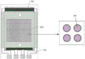
图10为本公开一些实施例提供的一种反应系统的检测芯片的平面示意图;10 is a schematic plan view of a detection chip of a reaction system provided by some embodiments of the present disclosure;
图11A为本公开一些实施例提供的一种反应系统进行热循环时温度与时间的关系曲线;11A is a relationship curve between temperature and time when a reaction system according to some embodiments of the present disclosure performs thermal cycling;
图11B为本公开一些实施例提供的一种反应系统进行热循环时包含预变性过程的温度与时间的关系曲线。FIG. 11B is a relationship curve between temperature and time including a pre-denaturation process when a reaction system according to some embodiments of the present disclosure is thermally cycled.
具体实施方式Detailed ways
为使本公开实施例的目的、技术方案和优点更加清楚,下面将结合本公开实施例的附图,对本公开实施例的技术方案进行清楚、完整地描述。显然,所描述的实施例是本公开的一部分实施例,而不是全部的实施例。基于所描述的本公开的实施例,本领域普通技术人员在无需创造性劳动的前提下所获得的所有其他实施例,都属于本公开保护的范围。In order to make the purpose, technical solutions and advantages of the embodiments of the present disclosure more clear, the technical solutions of the embodiments of the present disclosure will be clearly and completely described below with reference to the accompanying drawings of the embodiments of the present disclosure. Obviously, the described embodiments are some, but not all, embodiments of the present disclosure. Based on the described embodiments of the present disclosure, all other embodiments obtained by those of ordinary skill in the art without creative efforts fall within the protection scope of the present disclosure.
除非另外定义,本公开使用的技术术语或者科学术语应当为本公开所属领域内具有一般技能的人士所理解的通常意义。本公开中使用的“第一”、“第二”以及类似的词语并不表示任何顺序、数量或者重要性,而只是用来区分不同的组成部分。同样,“一个”、“一”或者“该”等类似词语也不表示数量限制,而是表示存在至少一个。“包括”或者“包含”等类似的词语意指出现该词前面的元件或者物件涵盖出现在该词后面列举的元件或者物件及其等同,而不排除其他元件或者物件。“连接”或者“相连”等类似的词语并非限定于物理的或者机械的连接,而是可以包括电性的连接,不管是直接的还是间接的。“上”、“下”、“左”、“右”等仅用于表示相对位置关系,当被描述对象的绝对位置改变后,则该相对位置关系也可能相应地改变。Unless otherwise defined, technical or scientific terms used in this disclosure shall have the ordinary meaning as understood by one of ordinary skill in the art to which this disclosure belongs. As used in this disclosure, "first," "second," and similar terms do not denote any order, quantity, or importance, but are merely used to distinguish the various components. Likewise, words such as "a," "an," or "the" do not denote a limitation of quantity, but rather denote the presence of at least one. "Comprises" or "comprising" and similar words mean that the elements or things appearing before the word encompass the elements or things recited after the word and their equivalents, but do not exclude other elements or things. Words like "connected" or "connected" are not limited to physical or mechanical connections, but may include electrical connections, whether direct or indirect. "Up", "Down", "Left", "Right", etc. are only used to represent the relative positional relationship, and when the absolute position of the described object changes, the relative positional relationship may also change accordingly.
在进行PCR反应时,DNA片段的双链结构在高温时变性形成单链结构,在低温时引物与单链按照碱基互补配对原则实现结合,在DNA聚合酶最适宜温度实现碱基结合延伸,上述过程即为变性-退火-延伸的温度循环过程。通过变性-退火-延伸的多个温度循环过程,DNA片段可实现大量复制。During the PCR reaction, the double-stranded structure of the DNA fragment is denatured at high temperature to form a single-stranded structure. At low temperature, the primer and the single-strand are combined according to the principle of base complementary pairing, and base binding and extension are realized at the optimal temperature of DNA polymerase. The above process is the temperature cycle process of denaturation-annealing-extension. Through multiple temperature cycles of denaturation-annealing-extension, DNA fragments can achieve large-scale replication.
为了实现上述温度循环过程,通常需要采用一系列的外部设备对检测芯片进行加热和冷却,使得设备体积庞大,需要多台设备配套使用,操作复杂,且成本较高。市售产品通常采用外部设备进行温度控制,其检测效率通常超过60分钟(20-30个循环),部分产品甚至高达90-120分钟(20-30个循环),因此检测效率较低。并且,对检测芯片进行加热和冷却的过程中,检测芯片的整体温度随之变化,使得检测芯片中除了容纳DNA片段的微腔以外的其他结构及部件的温度也随之变化,从而增加了例如电路等部件的损坏风险。In order to realize the above-mentioned temperature cycle process, a series of external equipments are usually used to heat and cool the detection chip, which makes the equipment bulky, requires multiple equipments to be used together, and the operation is complicated and the cost is high. Commercial products usually use external equipment for temperature control, and their detection efficiency is usually more than 60 minutes (20-30 cycles), and some products are even as high as 90-120 minutes (20-30 cycles), so the detection efficiency is low. In addition, in the process of heating and cooling the detection chip, the overall temperature of the detection chip changes accordingly, so that the temperature of other structures and components in the detection chip other than the microcavity for accommodating DNA fragments also changes accordingly, thereby increasing, for example, Risk of damage to components such as circuits.
本公开至少一实施例提供一种用于检测芯片的反应设备及反应系统,该反应设备可以实现高效、精确控温,控温方式简单,直插直读,操作简便,智能化、便携化和集成化程度高,检测效率高,能够实现高效、快速的数字 PCR检测。At least one embodiment of the present disclosure provides a reaction device and a reaction system for detecting chips. The reaction device can achieve efficient and accurate temperature control, simple temperature control, direct insertion and direct reading, easy operation, intelligence, portability and It has a high degree of integration and high detection efficiency, and can realize efficient and fast digital PCR detection.
下面,将参考附图详细地说明本公开的实施例。应当注意的是,不同的附图中相同的附图标记将用于指代已描述的相同的元件。Hereinafter, embodiments of the present disclosure will be described in detail with reference to the accompanying drawings. It should be noted that the same reference numerals will be used in different drawings to refer to the same elements that have been described.
本公开至少一实施例提供一种反应设备,该反应设备用于检测芯片,且包括芯片载台和电信号控制单元。芯片载台配置为放置和固定该检测芯片;电信号控制单元配置为对该检测芯片施加电信号,以驱动该检测芯片的加热电极。At least one embodiment of the present disclosure provides a reaction device, which is used for detecting a chip and includes a chip carrier and an electrical signal control unit. The chip stage is configured to place and fix the detection chip; the electric signal control unit is configured to apply an electric signal to the detection chip to drive the heating electrode of the detection chip.
图1为本公开一些实施例提供的一种反应设备的示意框图。如图1所示,该反应设备10包括芯片载台110和电信号控制单元120。例如,反应设备 10与另行提供的检测芯片配合工作以实现PCR反应(例如还可进一步实现 PCR检测),在工作过程中,该检测芯片中含有反应体系溶液,反应设备 10可向该检测芯片施加电信号使检测芯片升温,以使检测芯片中的反应体系溶液进行变性-退火-延伸的温度循环过程,从而使反应体系溶液中的DNA 片段实现大量复制。FIG. 1 is a schematic block diagram of a reaction apparatus provided by some embodiments of the present disclosure. As shown in FIG. 1 , the
例如,芯片载台110配置为放置和固定检测芯片,可以实现检测芯片的即插即用。电信号控制单元120配置为对检测芯片施加电信号(例如电压信号),以驱动检测芯片的加热电极。检测芯片的加热电极接收到电信号后,会释放热量,从而使检测芯片的功能区域升温,以达到进行温度循环过程的预设温度。For example, the
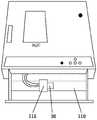
图2为本公开一些实施例提供的一种反应设备的外观示意图。如图2所示,该反应设备10还包括支架130。例如,支架130为该反应设备10的外壳和内部支撑结构,起支撑、保护等作用,还可以用于为该反应设备10的其他部件提供安装位置。例如,支架130可以由塑料、金属或其他任意适用的材料制备。FIG. 2 is a schematic diagram of the appearance of a reaction apparatus provided by some embodiments of the present disclosure. As shown in FIG. 2 , the
图3为本公开一些实施例提供的一种反应设备的芯片载台的示意图。如图2和图3所示,芯片载台110设置在支架130上,且与支架130滑动连接,可被拉出或推入支架130。当芯片载台110被拉出支架130时,芯片载台110 暴露在支架130之外,从而可以放置或取出检测芯片。当芯片载台110被推入支架130时,芯片载台110被包含在支架130的内部空间中,从而可以进行加热、冷却、光学检测等操作。FIG. 3 is a schematic diagram of a chip stage of a reaction apparatus provided by some embodiments of the present disclosure. As shown in FIG. 2 and FIG. 3 , the
例如,如图3所示,芯片载台110包括底板111、支撑部112、限位槽 113和至少一个限位块114。For example, as shown in FIG. 3 , the
例如,底板111配置为与支架130滑动连接,从而使芯片载台110可以被拉出或推入支架130。例如,底板111可以通过直线导轨与支架130连接,该直线导轨可以设置在底板111的两侧。需要说明的是,本公开的实施例中,底板111与支架130的连接方式不受限制,可以采用任意适用的连接方式,也可以采用任意适用的连接结构,这可以根据实际需求而定。For example, the
例如,在一些示例中,该反应设备10还可以包括驱动电机,该驱动电机配置为驱动底板111相对于支架130移动,从而可以实现检测芯片的自动载入,提高该反应设备10的自动化程度,减少人工操作。例如,该驱动电机可以与直线导轨中的滑块连接,滑块与底板111固定连接,直线导轨中的导轨与支架130固定连接,从而可以在驱动电机的驱动下使滑块沿着导轨做直线运动,以实现芯片载台110的拉出和推入。当然,本公开的实施例不限于此,该反应设备10中也可以不设置驱动电机,通过人工操作将芯片载台 110拉出或推入支架130,从而可以降低成本,减轻设备重量。For example, in some examples, the
例如,底板111包括镂空区域111a,支撑部112位于底板111的镂空区域111a中且配置为支撑检测芯片。例如,支撑部112的尺寸小于镂空区域 111a的尺寸,以使检测芯片放置在支撑部112上后还有部分表面积暴露于空气中,从而便于检测芯片散热,以便于进行温度控制。例如,支撑部112的尺寸可以根据实际需求而定,例如根据放置检测芯片的稳固程度和散热需求而定,本公开的实施例对此不作限制。For example, the
例如,限位槽113位于底板111的镂空区域111a的周围,且配置为防止检测芯片发生位移。例如,限位槽113的尺寸与检测芯片的尺寸相等或基本相等,从而更好地起限位作用,使检测芯片不易滑出限位槽113。当然,本公开的实施例不限于此,限位槽113的尺寸也可以略大于检测芯片的尺寸,这可以根据实际需求而定。例如,限位槽113的形状为近似的矩形,从而便于将矩形的检测芯片放置其中。例如,限位槽113还可以起支撑作用,与支撑部112共同支撑检测芯片。例如,为了留出人工操作的空间,便于用户抓握检测芯片,可以将限位槽113的一组彼此相对的边缘设置为具有圆弧形,且该圆弧形向彼此远离的方向凸起,从而为用户的手指留出空间,便于放置或取出检测芯片。For example, the limiting
例如,限位块114位于限位槽113的一侧,且配置为防止检测芯片发生翘曲。限位块114的数量不受限制,虽然图3中示出了2个限位块114的情形,但这并不构成对本公开实施例的限制。例如,限位块114也可以为1个、 3个或任意个数。例如,当检测芯片被放置在芯片载台110上时,需要使用夹具固定,且需要使夹具的接触电极与检测芯片的控制电极接触连接,因此检测芯片容易在夹具的压力下发生翘曲。通过设置限位块114,可以防止检测芯片翘曲,从而使检测芯片与夹具的连接更加牢固。关于夹具及其接触电极的详细说明可参考下文内容,此处不再赘述。For example, the limiting
图4为本公开一些实施例提供的一种反应设备的组件示意框图。如图4 所示,芯片载台110还包括夹具115,夹具115配置为可靠近或远离支撑部 112以使检测芯片与支撑部112的相对位置固定或可变。例如,检测芯片可以为图4所示的检测芯片30,该检测芯片30包括控制电极310和加热电极 320。将检测芯片30放置在芯片载台110上后,可以使夹具115靠近支撑部 112,从而使检测芯片30固定在芯片载台110上。当需要取出检测芯片30 时,使夹具115远离支撑部112,从而可以将检测芯片30从芯片载台110上取出。例如,可以通过人工操作的方式调节夹具115与支撑部112之间的距离,以使夹具115相对于支撑部112移动,也可以通过另行设置的动力部件 (例如电机)调节夹具115与支撑部112之间的距离,本公开的实施例对此不作限制。例如,在一些示例中,夹具115可以设置在支架130内,且位于芯片载台110的上方,并且可相对于芯片载台110上下移动。FIG. 4 is a schematic block diagram of components of a reaction apparatus provided by some embodiments of the present disclosure. As shown in FIG. 4 , the
例如,夹具115包括接触电极1151,接触电极1151配置为可与检测芯片30的控制电极310接触连接以实现电连接。将检测芯片30放置在芯片载台110上后,采用夹具115将检测芯片30固定,例如,夹具115与检测芯片30彼此接触,使得接触电极1151与控制电极310也实现接触连接,从而可以传输电信号。例如,接触电极1151可以采用金属材料制备,从而可以减小电阻,降低对信号驱动能力的要求。For example, the
例如,电信号控制单元120可以为如图4所示的功率放大电路121,该功率放大电路121可以输出较大功率的电压信号,可以直接驱动负载,带载能力较强。当然,本公开的实施例不限于此,电信号控制单元120也可以采用其他适用的电路或模块。电信号控制单元120与接触电极1151电连接,且配置为通过接触电极1151对检测芯片30的控制电极310施加电信号,以驱动检测芯片30的加热电极320。例如,电信号控制单元120输出的电信号通过电导线传输至接触电极1151,由于接触电极1151与控制电极310接触连接,因此电信号传输至控制电极310,进而传输至加热电极320。加热电极320在电信号的作用下产生并释放热量,使得检测芯片30的温度上升,从而实现加热的功能。For example, the electrical
例如,如图4所示,反应设备10还包括温度传感器140,温度传感器 140配置为可与检测芯片30接触以感测检测芯片30的温度。例如,如图3 所示,支撑部112包括凹槽1121,温度传感器140位于凹槽1121内(图3 中未示出温度传感器140)。当检测芯片30放置在芯片载台110上时,温度传感器140与检测芯片30直接接触,因此可以感测检测芯片30的温度。需要说明的是,本公开的实施例中,温度传感器140也可以不与检测芯片30 直接接触,而是具有一定间隙,温度传感器140的具体设置方式可以根据实际需求而定,例如根据温度传感器140的类型而定,本公开的实施例对此不作限制。For example, as shown in FIG. 4 , the
例如,温度传感器140可以为各种类型的温度传感器,例如,接触式温度传感器或非接触式温度传感器等,例如热电偶温度传感器或红外温度传感器等。例如,在一些示例中,温度传感器140为数字温度传感器,型号为 DS18B20,具有体积小、硬件开销低、抗干扰能力强、精度高等优点。需要说明的是,本公开的一些实施例中,若检测芯片30包括温度传感器,则反应设备10中无需再设置温度传感器140。For example, the
例如,如图4所示,反应设备10还包括降温单元150,降温单元150 配置为对检测芯片30降温。例如,降温单元150可以为风扇或风机,例如程序可控的风扇或风机,从而在实现降温功能的同时降低成本。例如,降温单元150设置在芯片载台110的上方或下方,从而可以加快散热速度。当需要对检测芯片30降温时,通过降温单元150实现风冷降温,从而使检测芯片30的温度降低。例如,通过电信号控制单元120和降温单元150的配合工作,可以使检测芯片30的温度根据需要升高或降低,从而实现温度控制,使检测芯片30内的反应体系溶液进行变性-退火-延伸的温度循环,以进行扩增反应。For example, as shown in FIG. 4 , the
例如,反应设备10还包括光学单元160,光学单元160配置为对检测芯片30进行光学检测。如图5所示,光学单元160包括光源161和图像传感器162。例如,光源161配置为发出光以照射检测芯片30,图像传感器162 配置为接收光源161发出且被检测芯片30反射的光。例如,光源161可以为激光器(例如激光波长为450nm-480nm)或荧光灯,图像传感器162可以为电荷耦合器件(CCD)图像传感器,本公开的实施例对此不作限制。当检测芯片30中的反应体系溶液完成扩增反应后,采用光学单元160对其进行光学检测,从而可以获得荧光图像,进而得到PCR检测结果。For example, the
例如,如图2和图4所示,反应设备10还包括交互单元170,交互单元 170配置为与用户进行交互。例如,交互单元170可以为触摸屏,该触摸屏配置为进行显示并进行触控检测以获取用户的输入指令。例如,该触摸屏可以为液晶(LCD)触摸屏、有机发光二极管(OLED)触摸屏、量子点发光二极管(QLED)触摸屏、电子纸触摸屏等,本公开的实施例对此不作限制。交互单元170还可以为其他形式的部件,例如为按键、显示屏、声音输入装置等,只要能实现与用户的交互即可。For example, as shown in Figures 2 and 4, the
例如,如图4所示,反应设备10还包括控制单元180,控制单元180 配置为对反应设备10的工作状态进行控制。例如,控制单元180可以运行控制程序,使电信号控制单元120输出电信号,控制降温单元150工作,接收温度传感器140传输的检测信号,控制交互单元170进行显示,接收用户通过交互单元170输入的指令等,控制单元180还可以具有其他功能,本公开的实施例对此不作限制。例如,控制单元180可以为单片机(MCU)、数字信号处理器(DSP)或现场可编程逻辑阵列(FPGA)等,本公开的实施例对此不作限制。例如,在一些示例中,控制单元180为STM32单片机。For example, as shown in FIG. 4 , the
例如,如图2和图4所示,反应设备10还包括存储单元190,存储单元 190配置为存储检测得到的数据和/或反应设备10的工作日志等。例如,存储单元190可以设置在支架130侧面的可活动安装槽131内,从而可以方便地拉出或推入支架130,以实现存储单元190的安装或取出。例如,存储单元190可以为各种形式的计算机可读存储介质,例如易失性存储器和/或非易失性存储器。易失性存储器例如可以包括随机存取存储器(RAM)和/或高速缓冲存储器(cache)等。非易失性存储器例如可以包括只读存储器(ROM)、硬盘、可擦除可编程只读存储器(EPROM)、便携式紧致盘只读存储器 (CD-ROM)、USB存储器、SD卡、闪存等。例如,存储单元190可以存储检测得到的数据,例如荧光图像和分析结果等,从而可以方便地进行检测结果的拷贝、传输等。存储单元190还可以用于存储反应设备10产生的任意的数据,例如反应设备10的工作日志、用户输入的指令等,本公开的实施例对此不作限制。For example, as shown in FIG. 2 and FIG. 4 , the
例如,如图4所示,反应设备10还包括电源210,电源210配置为对反应设备10供电。例如,电源210可以为外置电源的接口,通过导线、变压器等与供电网络电连接,或者可以为内置电源,例如二次电池(例如锂电池)、一次电池(例如碱性电池)、太阳能电池等任意适用的供电部件,本公开的实施例对此不作限制。For example, as shown in FIG. 4 , the
图6A-6D为本公开一些实施例提供的一种反应设备的操作界面示意图。图6A为开机欢迎界面,图6B为功能选择界面,图6C为参数设置界面,图 6D为温度曲线监测界面。例如,在功能选择界面,用户可以选择“SET”而进入参数设置界面,也可以选择“RUN”而执行温度循环过程并进入温度曲线监测界面。例如,在参数设置界面,用户可以设置温度循环过程各个阶段的温度,例如变性阶段的温度、退火阶段的温度和延伸阶段的温度,以及各个阶段的持续时间和温度循环次数等。6A-6D are schematic diagrams of operation interfaces of a reaction apparatus provided by some embodiments of the present disclosure. Fig. 6A is a boot welcome interface, Fig. 6B is a function selection interface, Fig. 6C is a parameter setting interface, and Fig. 6D is a temperature curve monitoring interface. For example, in the function selection interface, the user can select "SET" to enter the parameter setting interface, or select "RUN" to execute the temperature cycle process and enter the temperature curve monitoring interface. For example, in the parameter setting interface, the user can set the temperature of each stage of the temperature cycle process, such as the temperature of the denaturation stage, the temperature of the annealing stage and the temperature of the extension stage, as well as the duration of each stage and the number of temperature cycles.
需要说明的是,图6A-6D所示的操作界面仅是示意性的而非限制性的,反应设备10可以根据实际需求运行相应的控制程序并具有多个操作界面,各个操作界面呈现的信息可以根据实际需求而定。例如,在一些示例中,控制程序可以包括3个子程序,分别为操作系统、光学检测软件、图像拼接及数据读取软件,从而可以实现温度循环、光学检测等功能。例如,该控制程序可以存储在如图4所示的存储单元190中并被控制单元180执行,控制单元180将该控制程序的操作界面显示在交互单元170中。It should be noted that the operation interfaces shown in FIGS. 6A-6D are only schematic and non-limiting, and the
图7为本公开一些实施例提供的另一种反应设备的外观示意图之一,图 8为本公开一些实施例提供的另一种反应设备的外观示意图之二。如图7和图8所示,除了交互单元170的实现方式和反应设备10的外观不同外,该实施例的反应设备10与图2至图4所示的反应设备10基本相同。FIG. 7 is one of the schematic appearance diagrams of another reaction apparatus provided in some embodiments of the present disclosure, and FIG. 8 is the second schematic diagram of the appearance of another kind of reaction apparatus provided in some embodiments of the present disclosure. As shown in FIG. 7 and FIG. 8 , the
在该实施例中,交互单元170包括显示屏171和按键172。显示屏171 配置为进行显示,例如可以为LCD显示屏、OLED显示屏、QLED显示屏、电子纸显示屏等,本公开的实施例对此不作限制。按键172配置为获取用户的输入指令,例如可以为机械式按键、光学式按键等,本公开的实施例对此不作限制。例如,按键172可以包括程序控制开关1721、参数设置按钮1722、确认按钮1723、重置和步骤选择按钮1724。例如,通过参数设置按钮1722 可以设置检测过程中的各种参数,例如温度、时间等;通过重置和步骤选择按钮1724可以选择检测过程中的检测步骤。例如,该反应设备10还包括电源开关001,电源开关001用于控制该反应设备10开机或关机。In this embodiment, the
例如,存储单元190设置在反应设备10上表面的可开合安装槽内,将该可开合安装槽打开,即可方便地插入或取出存储单元190。例如,芯片载台110可被拉出或推入,检测芯片30可放置在芯片载台110上,并且通过夹具115固定。For example, the
需要说明的是,本公开的实施例中,反应设备10可以包括更多或更少的部件,这可以根据实际需要实现的功能和性能而定,本公开的实施例对此不作限制。上文描述的各个部件,例如芯片载台110、电信号控制单元120、支架130、温度传感器140、降温单位150、光学单元160、交互单元170、控制单元180、存储单元190和电源210等,可以采用任意适用的方式实现,只要能实现相应的功能即可,不限于上文描述的实现方式。It should be noted that, in the embodiments of the present disclosure, the
本公开至少一实施例还提供一种反应系统,该反应系统包括至少一个检测芯片和本公开任一实施例所述的可结合该至少一个检测芯片使用的反应设备。该反应系统可以实现高效、精确控温,控温方式简单,直插直读,操作简便,智能化、便携化和集成化程度高,检测效率高,能够实现高效、快速的数字PCR检测。At least one embodiment of the present disclosure further provides a reaction system, which includes at least one detection chip and the reaction device described in any embodiment of the present disclosure that can be used in combination with the at least one detection chip. The reaction system can realize efficient and precise temperature control, simple temperature control method, direct insertion and direct reading, easy operation, high degree of intelligence, portability and integration, high detection efficiency, and can realize efficient and fast digital PCR detection.
图9为本公开一些实施例提供的一种反应系统的示意框图。如图9所示,该反应系统40包括反应设备10和至少一个检测芯片30。例如,反应设备10为本公开任一实施例所述的反应设备。该反应系统可以包括一个或多个检测芯片30,例如这些检测芯片30可以为前述的任一检测芯片,这些检测芯片的规格可以彼此相同或不同。例如,如图10所示,检测芯片30包括多个微反应室330,微反应室330可容纳反应体系溶液。例如,在一些示例中,检测芯片30具有40万级反应单元,也即是,具有40万级微反应室330。检测芯片30的控制电极310可接收电信号并将该电信号传输至加热电极320。加热电极320在该电信号的作用下产生并释放热量,使检测芯片30的功能区域3001升温。反应设备10的电信号控制单元120向检测芯片30施加电信号以驱动检测芯片30的加热电极320,以使检测芯片30升温,反应设备 10的降温单元150使检测芯片30降温,以使反应体系溶液实现包括变性阶段、退火阶段和延伸阶段的温度循环。例如,反应设备10的光学单元160 可以对检测芯片30进行光学检测,以获得荧光图像。FIG. 9 is a schematic block diagram of a reaction system provided by some embodiments of the present disclosure. As shown in FIG. 9 , the
例如,该反应系统40进行PCR热循环扩增的过程如下。For example, the
将注入有反应体系溶液的检测芯片30放置在反应设备10的芯片载台 110上,并通过夹具115固定,使接触电极1151和检测芯片30的控制电极 310电连接。对反应设备10进行参数设置。例如,循环参数为95℃变性15 秒,55℃退火45秒,72℃延伸45秒,总共设置30个热循环。例如,还可以设置95℃预变性5分钟。检测芯片30中含有模板DNA的微反应室330 中的液滴会进行PCR扩增反应,而没有模板DNA的微反应室330中的液滴则作为对照组。例如,热循环的温度与时间的关系曲线如图11A和图11B 所示,可见,热循环的控温效果好,能够实现精确控温,控温精度达到0.5℃,并且检测时间短(30个循环用时35分钟),检测效率高。The
热循环扩增结束后,采用反应设备10的光学单元160对检测芯片30进行光学检测,从而得到荧光图像。该反应系统40能够使检测芯片30中的反应体系溶液进行有效的热循环扩增并得到清晰的荧光图像,检测通量高。After the thermal cycle amplification is completed, the optical unit 160 of the
需要说明的是,本公开的一些实施例中,反应系统40还可以包括更多的组件或部件,本公开的实施例对此不作限制。关于该反应系统40的详细说明和技术效果可参见上文中关于反应设备10的描述,此处不再赘述。It should be noted that, in some embodiments of the present disclosure, the
有以下几点需要说明:The following points need to be noted:
(1)本公开实施例附图只涉及到本公开实施例涉及到的结构,其他结构可参考通常设计。(1) The drawings of the embodiments of the present disclosure only relate to the structures involved in the embodiments of the present disclosure, and other structures may refer to general designs.
(2)在不冲突的情况下,本公开的实施例及实施例中的特征可以相互组合以得到新的实施例。(2) The embodiments of the present disclosure and features in the embodiments may be combined with each other to obtain new embodiments without conflict.
以上所述,仅为本公开的具体实施方式,但本公开的保护范围并不局限于此,本公开的保护范围应以所述权利要求的保护范围为准。The above descriptions are only specific embodiments of the present disclosure, but the protection scope of the present disclosure is not limited thereto, and the protection scope of the present disclosure should be subject to the protection scope of the claims.
Claims (20)
Priority Applications (5)
| Application Number | Priority Date | Filing Date | Title |
|---|---|---|---|
| CN201920470599.3UCN209974747U (en) | 2019-04-09 | 2019-04-09 | Reaction equipment and reaction system for detection chips |
| EP20787410.8AEP3954754A4 (en) | 2019-04-09 | 2020-03-31 | Reaction device and reaction system for detection chip |
| US17/254,984US11883822B2 (en) | 2019-04-09 | 2020-03-31 | Reaction device for detection chip and reaction system |
| PCT/CN2020/082402WO2020207295A1 (en) | 2019-04-09 | 2020-03-31 | Reaction device and reaction system for detection chip |
| JP2020572760AJP7568515B2 (en) | 2019-04-09 | 2020-03-31 | Reaction device and reaction system for detection chip |
Applications Claiming Priority (1)
| Application Number | Priority Date | Filing Date | Title |
|---|---|---|---|
| CN201920470599.3UCN209974747U (en) | 2019-04-09 | 2019-04-09 | Reaction equipment and reaction system for detection chips |
Publications (1)
| Publication Number | Publication Date |
|---|---|
| CN209974747Utrue CN209974747U (en) | 2020-01-21 |
Family
ID=69257171
Family Applications (1)
| Application Number | Title | Priority Date | Filing Date |
|---|---|---|---|
| CN201920470599.3UActiveCN209974747U (en) | 2019-04-09 | 2019-04-09 | Reaction equipment and reaction system for detection chips |
Country Status (5)
| Country | Link |
|---|---|
| US (1) | US11883822B2 (en) |
| EP (1) | EP3954754A4 (en) |
| JP (1) | JP7568515B2 (en) |
| CN (1) | CN209974747U (en) |
| WO (1) | WO2020207295A1 (en) |
Cited By (8)
| Publication number | Priority date | Publication date | Assignee | Title |
|---|---|---|---|---|
| WO2020207295A1 (en)* | 2019-04-09 | 2020-10-15 | 京东方科技集团股份有限公司 | Reaction device and reaction system for detection chip |
| CN113583799A (en)* | 2020-04-30 | 2021-11-02 | 京东方科技集团股份有限公司 | Analysis device for detecting chip, operation method thereof and analysis system |
| CN113583800A (en)* | 2020-04-30 | 2021-11-02 | 京东方科技集团股份有限公司 | Detection chip, use method thereof and reaction system |
| CN113773952A (en)* | 2021-10-12 | 2021-12-10 | 江苏汇先医药技术有限公司 | A handheld LAMP detector and system |
| CN114585987A (en)* | 2020-09-29 | 2022-06-03 | 京东方科技集团股份有限公司 | Temperature control device and temperature control system |
| WO2022226868A1 (en)* | 2021-04-29 | 2022-11-03 | 京东方科技集团股份有限公司 | Chip loading structure, analysis device and analysis system |
| US11654435B2 (en) | 2019-03-29 | 2023-05-23 | Boe Technology Group Co., Ltd. | Detection chip, method for operating detection chip, and reaction system |
| CN118813399A (en)* | 2023-04-18 | 2024-10-22 | 广州国家实验室 | Nucleic acid amplification device and nucleic acid amplification system |
Families Citing this family (2)
| Publication number | Priority date | Publication date | Assignee | Title |
|---|---|---|---|---|
| CN216274121U (en)* | 2021-10-12 | 2022-04-12 | 江苏汇先医药技术有限公司 | Handheld LAMP detector and system |
| TWI784808B (en)* | 2021-11-23 | 2022-11-21 | 敦泰電子股份有限公司 | Cascade synchronizer of touch display detection chips and touch display device |
Family Cites Families (12)
| Publication number | Priority date | Publication date | Assignee | Title |
|---|---|---|---|---|
| US6720187B2 (en) | 2000-06-28 | 2004-04-13 | 3M Innovative Properties Company | Multi-format sample processing devices |
| AU2003228514A1 (en) | 2002-04-11 | 2003-10-27 | Sequenom, Inc. | Methods and devices for performing chemical reactions on a solid support |
| JP6138684B2 (en) | 2010-08-31 | 2017-05-31 | キヤノン ユー.エス. ライフ サイエンシズ, インコーポレイテッドCanon U.S. Life Sciences, Inc. | Compositions and methods for in-system priming of microfluidic devices |
| US9114399B2 (en)* | 2010-08-31 | 2015-08-25 | Canon U.S. Life Sciences, Inc. | System and method for serial processing of multiple nucleic acid assays |
| KR101441594B1 (en) | 2012-12-27 | 2014-09-23 | 매쓰파워 주식회사 | Heat sensitive polymer composite based Nucleic Acid Amplification disc apparatus and analysis method using the same |
| ITTO20130940A1 (en)* | 2013-11-20 | 2015-05-21 | St Microelectronics Srl | KIT FOR BIOCHEMICAL ANALYSIS AND METHOD TO PERFORM A IMPROVED BIOCHEMICAL PROCESS |
| CN105861293B (en) | 2016-04-06 | 2017-11-07 | 深圳市瀚海基因生物科技有限公司 | Unimolecule gene sequencer |
| CN106222068A (en) | 2016-08-22 | 2016-12-14 | 上海交通大学 | Miniature PCR system of capillary glass tube and preparation method thereof |
| WO2019046860A1 (en)* | 2017-09-01 | 2019-03-07 | Miroculus Inc. | Digital microfluidics devices and methods of using them |
| CN109234158B (en)* | 2018-10-08 | 2021-08-06 | 北京京东方技术开发有限公司 | Biochip and its manufacturing method, operating method, and biological detection system |
| CN109289949B (en)* | 2018-10-15 | 2024-03-08 | 苏州锐讯生物科技有限公司 | Full-automatic micro-droplet emulsion generation device and generation method thereof |
| CN209974747U (en)* | 2019-04-09 | 2020-01-21 | 北京京东方技术开发有限公司 | Reaction equipment and reaction system for detection chips |
- 2019
- 2019-04-09CNCN201920470599.3Upatent/CN209974747U/enactiveActive
- 2020
- 2020-03-31JPJP2020572760Apatent/JP7568515B2/enactiveActive
- 2020-03-31USUS17/254,984patent/US11883822B2/enactiveActive
- 2020-03-31EPEP20787410.8Apatent/EP3954754A4/enactivePending
- 2020-03-31WOPCT/CN2020/082402patent/WO2020207295A1/ennot_activeCeased
Cited By (23)
| Publication number | Priority date | Publication date | Assignee | Title |
|---|---|---|---|---|
| US11654435B2 (en) | 2019-03-29 | 2023-05-23 | Boe Technology Group Co., Ltd. | Detection chip, method for operating detection chip, and reaction system |
| WO2020207295A1 (en)* | 2019-04-09 | 2020-10-15 | 京东方科技集团股份有限公司 | Reaction device and reaction system for detection chip |
| US11883822B2 (en) | 2019-04-09 | 2024-01-30 | Beijing Boe Technology Development Co., Ltd. | Reaction device for detection chip and reaction system |
| CN113583800B (en)* | 2020-04-30 | 2024-09-27 | 京东方科技集团股份有限公司 | Detection chip, use method thereof and reaction system |
| CN113583799A (en)* | 2020-04-30 | 2021-11-02 | 京东方科技集团股份有限公司 | Analysis device for detecting chip, operation method thereof and analysis system |
| JP7671701B2 (en) | 2020-04-30 | 2025-05-02 | 京東方科技集團股▲ふん▼有限公司 | Analytical device for use in test chips, its operating method, and analytical system |
| US12233411B2 (en) | 2020-04-30 | 2025-02-25 | Boe Technology Group Co., Ltd. | Detection chip, method of using detection chip and reaction system |
| CN113583799B (en)* | 2020-04-30 | 2024-11-26 | 京东方科技集团股份有限公司 | Analytical device for detecting chip, operating method thereof, and analytical system |
| WO2021218443A1 (en)* | 2020-04-30 | 2021-11-04 | 京东方科技集团股份有限公司 | Analysis apparatus for test chip and operation method for analysis apparatus, and analysis system |
| JP2023523376A (en)* | 2020-04-30 | 2023-06-05 | 京東方科技集團股▲ふん▼有限公司 | Analysis device used for test chip, its operation method, and analysis system |
| JP2023523661A (en)* | 2020-04-30 | 2023-06-07 | 京東方科技集團股▲ふん▼有限公司 | Inspection chip, usage thereof, and reaction system |
| EP4144438A4 (en)* | 2020-04-30 | 2023-10-25 | BOE Technology Group Co., Ltd. | Detection chip and usage method therefor, and reaction system |
| CN113583800A (en)* | 2020-04-30 | 2021-11-02 | 京东方科技集团股份有限公司 | Detection chip, use method thereof and reaction system |
| CN114585987A (en)* | 2020-09-29 | 2022-06-03 | 京东方科技集团股份有限公司 | Temperature control device and temperature control system |
| CN115735005A (en)* | 2021-04-29 | 2023-03-03 | 京东方科技集团股份有限公司 | Chip mounting structure, analysis device, and analysis system |
| WO2022226868A1 (en)* | 2021-04-29 | 2022-11-03 | 京东方科技集团股份有限公司 | Chip loading structure, analysis device and analysis system |
| US12390807B2 (en) | 2021-04-29 | 2025-08-19 | Beijing Boe Technology Development Co., Ltd. | Chip loading structure, analysis device, and analysis system |
| CN113930322B (en)* | 2021-10-12 | 2024-03-08 | 江苏汇先医药技术有限公司 | LAMP detector and control method |
| CN113773952A (en)* | 2021-10-12 | 2021-12-10 | 江苏汇先医药技术有限公司 | A handheld LAMP detector and system |
| CN113930322A (en)* | 2021-10-12 | 2022-01-14 | 江苏汇先医药技术有限公司 | LAMP detector and control method |
| CN113773952B (en)* | 2021-10-12 | 2025-09-23 | 江苏汇先医药技术有限公司 | A handheld LAMP detector and system |
| CN118813399A (en)* | 2023-04-18 | 2024-10-22 | 广州国家实验室 | Nucleic acid amplification device and nucleic acid amplification system |
| WO2024217048A1 (en)* | 2023-04-18 | 2024-10-24 | 广州国家实验室 | Nucleic acid amplification device and nucleic acid amplification system |
Also Published As
| Publication number | Publication date |
|---|---|
| JP7568515B2 (en) | 2024-10-16 |
| EP3954754A4 (en) | 2023-02-01 |
| JP2022527876A (en) | 2022-06-07 |
| US20210268504A1 (en) | 2021-09-02 |
| US11883822B2 (en) | 2024-01-30 |
| WO2020207295A1 (en) | 2020-10-15 |
| EP3954754A1 (en) | 2022-02-16 |
Similar Documents
| Publication | Publication Date | Title |
|---|---|---|
| CN209974747U (en) | Reaction equipment and reaction system for detection chips | |
| US20250161948A1 (en) | Portable devices and methods for analyzing samples | |
| US11892461B1 (en) | Portable devices and methods for analyzing samples | |
| US20240132945A1 (en) | Multi-function analytic devices | |
| CN103189141B (en) | thermal cycler | |
| CN109957506B (en) | Device for quantitative polymerase chain reaction by thermal convection through reagent container | |
| CN102654558A (en) | Light-emitting diode (LED) testing device | |
| US20230160823A1 (en) | Analysis device for detection chip and method of operating thereof, and analysis system | |
| US20230249189A1 (en) | Ultra-Fast PCR Thermocycler | |
| CN212581920U (en) | Detection system for detection of alcohol metabolism-related genes | |
| CN216513850U (en) | Portable array nucleic acid amplicon signal detection device | |
| CN213012879U (en) | PCR augmentor | |
| CN212640438U (en) | A nucleic acid detection device for meat-derived samples based on hydroxynaphthol blue indicator | |
| TW201928045A (en) | Convective PCR apparatus | |
| CN113528312A (en) | Convection current PCR amplification check out test set | |
| Pan et al. | Portable loop-mediated isothermal amplification device with spectrometric detection for rapid pathogen identification | |
| CN113549698A (en) | Primer group, probe group, detection method and system for detecting alcohol metabolism related gene | |
| CN221854624U (en) | Nucleic acid amplification detection equipment based on micro-fluidic chip | |
| CN223016807U (en) | Clamping mechanism, temperature control circulating device and PCR analyzer | |
| CN216192353U (en) | Nucleic acid amplification device for nucleic acid detection | |
| CN118546774B (en) | Real-time fluorescence PCR analyzer and detection method thereof | |
| CN221028439U (en) | Portable nucleic acid detecting device | |
| WO2022044054A1 (en) | A system for carrying out rapid detection of pathogens | |
| CN118813762A (en) | A real-time quantitative detection method and detection instrument for nucleic acid amplification products |
Legal Events
| Date | Code | Title | Description |
|---|---|---|---|
| GR01 | Patent grant | ||
| GR01 | Patent grant |