CN203454973U - Sealing glue detection apparatus and display panel box forming apparatus - Google Patents
Sealing glue detection apparatus and display panel box forming apparatusDownload PDFInfo
- Publication number
- CN203454973U CN203454973UCN201320582044.0UCN201320582044UCN203454973UCN 203454973 UCN203454973 UCN 203454973UCN 201320582044 UCN201320582044 UCN 201320582044UCN 203454973 UCN203454973 UCN 203454973U
- Authority
- CN
- China
- Prior art keywords
- plastic box
- sealed plastic
- frame
- substrate
- sealant
- Prior art date
- Legal status (The legal status is an assumption and is not a legal conclusion. Google has not performed a legal analysis and makes no representation as to the accuracy of the status listed.)
- Expired - Lifetime
Links
Images

Landscapes
- Length Measuring Devices By Optical Means (AREA)
Abstract
Translated fromChinese
Description
Translated fromChinese技术领域technical field
本实用新型属于显示技术领域,具体涉及一种封框胶检测装置以及显示面板成盒设备。The utility model belongs to the field of display technology, in particular to a frame sealing glue detection device and display panel box forming equipment.
背景技术Background technique
随着科技的进步,液晶显示器(Liquid Crystal Display,简称LCD)已经成为显示领域的主流产品,在生产工艺中通过将阵列基板和彩膜基板对盒可以形成液晶显示面板。With the advancement of technology, Liquid Crystal Display (LCD for short) has become a mainstream product in the display field. In the production process, the liquid crystal display panel can be formed by combining the array substrate and the color filter substrate.
在成盒工艺中,主要包括:封框胶涂布、固化、对位检测、切割步骤。为了保证封框胶在真空对盒过程中具有足够的耐冲击力,在成盒工艺中一般还包括封框胶的尺寸检测步骤,但现有技术对封框胶的尺寸检测通常仅包括宽度检测,如图1所示为现有技术中封框胶检测装置的结构示意图。图1中,封框胶检测装置包括固定不动的机架(Gantry)10和基台(Stage)11,基台11的两侧分别设置有传送带(Transfer)16,机架10对应着基台11的上方还设置有检测头13,检测头13中包括封框胶宽度测量模块14以及修补器15(Repairing Head),封框胶宽度测量模块14包括CCD相机(CCD Camera)。在检测过程中,由传送带16带动未经切割的显示面板12(例如阵列基板)在基台11上沿Y轴方向移动,在阵列基板多次沿Y轴方向来回运动的同时,CCD相机沿X轴方向移动,从而对阵列基板上所有描画后的封框胶的宽度进行检测,并判断是否出现断胶(或断线)现象。一旦出现断胶(或断线)现象,则修补器15将根据记录的封框胶断线位置对相应位置进行补画封框胶。In the box forming process, it mainly includes: frame sealing glue coating, curing, alignment detection, and cutting steps. In order to ensure that the frame sealant has sufficient impact resistance during the vacuum box alignment process, the size detection step of the frame sealant is generally included in the box forming process, but the size detection of the frame sealant in the prior art usually only includes width detection. , as shown in FIG. 1 is a schematic structural diagram of a frame sealant detection device in the prior art. In Fig. 1, the frame sealant detection device includes a fixed frame (Gantry) 10 and abutment (Stage) 11, the two sides of the abutment 11 are respectively provided with conveyor belts (Transfer) 16, and the
在成盒工艺中,涂布于阵列基板上的封框胶,具有将阵列基板和彩膜基板粘合在一起并进行密封的作用,若其描画后的湿面积(由与阵列基板板面垂直的纵截面的宽度和厚度共同决定的面积)未能达到要求,在真空对盒过程中由于气体的冲击,可能造成封框胶崩溃,从而导致出现气泡,严重的甚至导致液晶泄露。但是,如前所述,现有的封框胶检测装置仅能检测封框胶描画后的宽度及是否断胶,无法检测封框胶的厚度。因此,在封框胶宽度合格的情况下,封框胶的厚度将直接反映封框胶的描画品质,决定着液晶面板的成盒良率。In the box forming process, the sealant coated on the array substrate has the function of bonding the array substrate and the color filter substrate together and sealing them. If the wet area after drawing (by perpendicular to the array substrate surface) The area determined by the width and thickness of the longitudinal section) fails to meet the requirements. Due to the impact of gas during the vacuum boxing process, the sealing glue may collapse, resulting in bubbles, and even liquid crystal leakage. However, as mentioned above, the existing frame sealant detection device can only detect the width of the frame sealant after drawing and whether the glue is broken, but cannot detect the thickness of the frame sealant. Therefore, when the width of the sealant is qualified, the thickness of the sealant will directly reflect the drawing quality of the sealant and determine the yield rate of the LCD panel.
因此,在封框胶宽度检测的同时,对封框胶描画后的厚度变化进行监控,成为目前亟待解决的问题。Therefore, while detecting the width of the sealant, monitoring the thickness change of the sealant after drawing has become an urgent problem to be solved.
实用新型内容Utility model content
本实用新型所要解决的技术问题是针对现有技术中存在的上述不足,提供一种封框胶检测装置以及显示面板成盒设备,该封框胶检测装置能实现全面监控封框胶的描画品质,提高封框胶的描画良率,提高显示面板(Panel)的良率。The technical problem to be solved by the utility model is to provide a frame sealing glue detection device and a display panel box forming equipment for the above-mentioned deficiencies in the prior art. The frame sealing glue detection device can realize comprehensive monitoring of the drawing quality of the frame sealing glue , improve the drawing yield of the sealant, and improve the yield of the display panel (Panel).
解决本实用新型技术问题所采用的技术方案是该封框胶检测装置,用于对形成在基板上的封框胶的尺寸进行检测,所述封框胶检测装置包括机架以及设置于所述机架上的检测头,所述机架下方对应的区域为待测基板放置区,其中,所述检测头包括至少一个封框胶厚度检测模块,所述封框胶厚度检测模块与所述待测基板放置区相对设置。The technical solution adopted to solve the technical problems of the utility model is the frame sealant detection device, which is used to detect the size of the frame sealant formed on the substrate. The frame sealant detection device includes a frame and is arranged on the The detection head on the frame, the corresponding area under the frame is the substrate placement area to be tested, wherein the detection head includes at least one frame sealant thickness detection module, and the frame sealant thickness detection module is connected to the to-be-tested substrate The test substrate placement area is relatively set.
优选的是,所述封框胶检测装置还包括处理器,所述封框胶厚度检测模块包括光发射器、光接收透镜和光接收器,所述光发射器与所述光接收器相离设置于所述待测基板放置区的上方、且分别与所述处理器电连接;所述处理器设置为根据所述待测基板表面与其上的封框胶表面通过所述光接收器形成的成像点的距离差获得封框胶的厚度。Preferably, the frame sealant detection device further includes a processor, the frame sealant thickness detection module includes a light emitter, a light receiving lens and a light receiver, and the light emitter is set apart from the light receiver above the placement area of the substrate to be tested, and are electrically connected to the processors respectively; The distance difference between the points obtains the thickness of the sealant.
优选的是,所述封框胶厚度检测模块还包括光调节透镜,所述光调节透镜设置于所述光发射器与所述待测基板放置区之间,所述光调节透镜光轴与所述光发射器平面垂直。Preferably, the frame sealant thickness detection module further includes a light adjustment lens, the light adjustment lens is arranged between the light emitter and the placement area of the substrate to be tested, and the optical axis of the light adjustment lens is in line with the The plane of the light emitter is vertical.
优选的是,所述封框胶厚度检测模块还包括滤光片,所述滤光片设置于所述光接收透镜与所述待测基板放置区之间,所述滤光片平面与所述光接收透镜主平面平行。Preferably, the frame sealant thickness detection module further includes an optical filter, the optical filter is arranged between the light receiving lens and the placement area of the substrate to be tested, and the plane of the optical filter is in contact with the The principal planes of the light receiving lenses are parallel.
优选的是,所述光发射器相对所述待测基板放置区水平/倾斜设置于所述待测基板放置区的上方;和/或,所述光接收器相对所述待测基板放置区平面水平/倾斜设置于所述待测基板放置区的上方。Preferably, the light emitter is arranged horizontally/inclined above the placement area of the substrate to be tested relative to the placement area of the substrate to be tested; and/or, the light receiver is flat relative to the placement area of the substrate to be tested The horizontal/tilt is arranged above the placement area of the substrate to be tested.
优选的是,所述光发射器为半导体激光发射器,所述光调节透镜为准直透镜,所述光接收透镜为双胶合透镜,所述光接收器为线性电荷耦合元件阵列。Preferably, the light transmitter is a semiconductor laser transmitter, the light adjustment lens is a collimator lens, the light receiving lens is a doublet lens, and the light receiver is a linear charge-coupled element array.
优选的是,每一所述检测头包括两个所述封框胶厚度检测模块,分别用于对所述封框胶在互相垂直的两个方向上的厚度的检测。Preferably, each of the detection heads includes two thickness detection modules of the sealant, which are respectively used to detect the thickness of the sealant in two directions perpendicular to each other.
优选的是,所述检测头还包括封框胶宽度检测模块,所述封框胶宽度检测模块与所述处理器电连接。Preferably, the detection head further includes a frame sealant width detection module, and the frame sealant width detection module is electrically connected to the processor.
优选的是,所述封框胶检测装置还包括与所述机架相对设置的基台,所述待测基板放置区为所述基台台面,所述封框胶检测装置还包括伺服马达,所述伺服马达设置于所述机架的底部,所述机架随所述伺服马达沿Y轴方向移动;和/或,所述伺服马达设置于所述基台的底部,所述基台随所述伺服马达沿X轴移动,其中,所述Y轴与所述X轴垂直。Preferably, the frame sealant detection device further includes a base set opposite to the frame, the substrate-to-be-test placement area is the base table, and the frame sealant detection device further includes a servo motor, The servo motor is arranged at the bottom of the frame, and the frame moves along the Y-axis direction with the servo motor; and/or, the servo motor is arranged at the bottom of the base, and the base moves with the The servo motor moves along an X axis, wherein the Y axis is perpendicular to the X axis.
一种显示面板成盒设备,包括上述的封框胶检测装置。A display panel box forming device, comprising the above-mentioned frame sealant detection device.
本实用新型的有益效果是:本实用新型的封框胶检测装置,在对描画后的封框胶进行宽度测量的同时,还能对描画后的封框胶厚度进行实时、准确地测量,从而实现全面监控封框胶的描画品质,提高封框胶的描画良率,提高显示面板(Panel)的良率。The beneficial effects of the utility model are: the frame sealing glue detection device of the utility model can measure the thickness of the drawn sealing glue in real time and accurately while measuring the width of the drawn sealing glue, thereby Realize comprehensive monitoring of the drawing quality of the sealant, improve the drawing yield of the sealant, and improve the yield of the display panel (Panel).
附图说明Description of drawings
图1为现有技术中封框胶检测装置的结构示意图;Fig. 1 is a structural schematic diagram of a frame sealing glue detection device in the prior art;
图2为本实用新型实施例1中封框胶检测装置的结构示意图;Fig. 2 is a schematic structural diagram of a frame sealing glue detection device in Embodiment 1 of the present utility model;
图3为本实用新型实施例1中封框胶厚度检测模块的结构示意图;Fig. 3 is a schematic structural diagram of the detection module for the thickness of the sealing glue in Embodiment 1 of the present utility model;
图4为本实用新型实施例2中封框胶厚度检测模块的结构示意图;Fig. 4 is a schematic structural diagram of a frame sealing glue thickness detection module in Embodiment 2 of the present invention;
图中:1-半导体激光发射器;2-准直透镜;3-双胶合透镜;4-线性CCD阵列;5-滤光片;6-参考面;7-实际面;8-处理器;10-机架;11-基台;12-显示面板;13-检测头;14-封框胶宽度测量模块;15-修补器;16-传送带;17-封框胶厚度测量模块;18-伺服马达。In the figure: 1-semiconductor laser emitter; 2-collimator lens; 3-doublet lens; 4-linear CCD array; 5-filter; 6-reference plane; 7-actual plane; 8-processor; 10 -frame; 11-abutment; 12-display panel; 13-detection head; 14-sealant width measurement module; 15-patcher; 16-conveyor belt; 17-sealant thickness measurement module; 18-servo motor .
具体实施方式Detailed ways
为使本领域技术人员更好地理解本实用新型的技术方案,下面结合附图和具体实施方式对本实用新型封框胶检测装置以及显示面板成盒设备作进一步详细描述。In order to enable those skilled in the art to better understand the technical solution of the present invention, the frame sealing glue detection device and the display panel box forming equipment of the present invention will be further described in detail below with reference to the accompanying drawings and specific embodiments.
一种封框胶检测装置,用于对形成在基板上的封框胶的尺寸进行检测,所述封框胶检测装置包括机架以及设置于所述机架上的检测头,所述机架下方对应的区域为待测基板放置区,其中,所述检测头包括至少一个封框胶厚度检测模块,所述封框胶厚度检测模块与所述待测基板放置区相对设置。A frame sealant detection device for detecting the size of a frame sealant formed on a substrate, the frame sealant detection device comprising a frame and a detection head arranged on the frame, the frame The corresponding area below is the substrate-to-be-tested placement area, wherein the detection head includes at least one frame sealant thickness detection module, and the frame sealant thickness detection module is arranged opposite to the substrate-to-be-test placement area.
实施例1:Example 1:
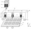
如图2、3所示,本实施例中,一种封框胶检测装置,用于对形成在基板上的封框胶的尺寸进行检测。该封框胶检测装置包括处理器8、以及相对设置的机架10和基台11,机架10对应着基台11的上方设置有检测头13,检测头13包括封框胶宽度检测模块14,封框胶厚度检测模块17与基台台面相对设置,且封框胶宽度检测模块14与处理器8电连接,其中,检测头13还包括至少一个封框胶厚度检测模块17,封框胶厚度检测模块17与处理器8电连接。其中,机架10下方对应的区域为待测基板放置区,即图2中与机架10相对设置的基台台面为待测基板放置区,用于放置待测基板。As shown in FIGS. 2 and 3 , in this embodiment, a frame sealant detection device is used to detect the size of the frame sealant formed on the substrate. The frame sealant detection device includes a processor 8, and a
本实施例中,利用光学透镜对封框胶的表面进行成像,从而对封框胶的表面位置进行检测,并通过处理器计算来获得封框胶的厚度。例如,本实施例中封框胶厚度检测模块17包括光发射器、光接收透镜和光接收器,光发射器与光接收器相离设置于基台的上方、且分别与处理器8电连接。其中,处理器8设置为根据待测基板表面与其上的封框胶表面通过光接收器形成的成像点的距离差获得封框胶的厚度In this embodiment, an optical lens is used to image the surface of the sealant, thereby detecting the surface position of the sealant, and the thickness of the sealant is obtained through calculation by a processor. For example, the frame sealant
在本实施例中,优选采用激光成像对待测基板表面或待测封框胶表面进行成像。如图3所示,优选光发射器为半导体激光发射器1,光接收透镜(也即成像透镜)为双胶合透镜3,光接收器为线性CCD(Charge-Coupled Device,电荷耦合元件)阵列4(也简称线阵CCD)。其中,半导体激光发射器1用于发射激光,作为检测光束;双胶合透镜3由两种不同折射率的正、负透镜胶合而成,且对轴上和近轴点已矫正了球差色差,具有短焦长、大放大率和较好成像质量的优点;线性CCD阵列4中,CCD采用高感光度的半导体材料集成,能够根据照射在其面上的光线产生相应的电荷信号,通过模数转换器芯片转换成“0”或“1”的数字信号,根据这些数字信号可对待测基板或待测封框胶的位置进行准确的测量、分析。In this embodiment, laser imaging is preferably used to image the surface of the substrate to be tested or the surface of the sealant to be tested. As shown in Figure 3, the preferred light transmitter is a semiconductor laser transmitter 1, the light receiving lens (that is, the imaging lens) is a doublet lens 3, and the light receiver is a linear CCD (Charge-Coupled Device, charge-coupled device) array 4 (Also referred to as linear array CCD). Among them, the semiconductor laser transmitter 1 is used to emit laser light as a detection beam; the doublet lens 3 is made of two kinds of positive and negative lenses with different refractive indices glued together, and the spherical aberration and chromatic aberration have been corrected for the axial and paraxial points, It has the advantages of short focal length, large magnification and better imaging quality; in the linear CCD array 4, the CCD is integrated with high-sensitivity semiconductor materials, which can generate corresponding charge signals according to the light irradiated on its surface, and pass the modulus The converter chip converts the digital signal of "0" or "1", and according to these digital signals, the position of the substrate to be tested or the sealant to be tested can be accurately measured and analyzed.
进一步优选的,封框胶厚度检测模块17还包括光调节透镜,光调节透镜设置于半导体激光发射器1与基台11台面之间,光调节透镜光轴与半导体激光发射器1平面垂直。通过光调节透镜,可以对半导体激光发射器1发出的检测光束的传播方向进行调整,以使得检测光束在待测基板表面或待测封框胶表面获得更好的入射角。在本实施例中,如图3所示,光调节透镜为准直透镜2,准直透镜2主要用于产生平行光束,优选经准直透镜2调节后的检测光束垂直入射至基台台面,也即垂直入射至待测基板表面(对应图3中的参考面6)或待测封框胶表面(对应图3中的实际面7)。Further preferably, the frame sealant
更进一步优选的,如图3所示,封框胶厚度检测模块还包括滤光片5,滤光片5设置于光接收透镜与基台台面之间,滤光片5平面与光接收透镜主平面平行。通过滤光片5,可以对非反射光束以外的其他可见光进行过滤,以避免成像干扰。More preferably, as shown in Figure 3, the frame sealant thickness detection module also includes a filter 5, the filter 5 is arranged between the light-receiving lens and the base table, the plane of the filter 5 and the main surface of the light-receiving lens plane parallel. Visible light other than the non-reflected light beam can be filtered by the filter 5 to avoid imaging interference.
在本实施例中,如图3所示,半导体激光发射器1相对基台台面水平设置于基台11的上方,双胶合透镜3相对基台台面水平设置于基台11的上方,半导体激光发射器平面、准直透镜主平面、基台台面互相平行,半导体激光发射器发出的检测光束沿半导体激光发射器的法线方向发出(即检测光束与半导体激光发射器的法线夹角为0°);经基台台面反射后的反射光束与半导体激光发射器光轴的夹角为α,相应的成像光束与线性CCD阵列平面的夹角为β,其中,α+β=90°。In this embodiment, as shown in Figure 3, the semiconductor laser emitter 1 is horizontally arranged above the base 11 relative to the base table, the doublet lens 3 is horizontally arranged above the base 11 relative to the base table, and the semiconductor laser emitter The plane of the detector, the main plane of the collimating lens, and the surface of the abutment are parallel to each other, and the detection beam emitted by the semiconductor laser emitter is emitted along the normal direction of the semiconductor laser emitter (that is, the angle between the detection beam and the normal of the semiconductor laser emitter is 0° ); the included angle between the reflected beam reflected by the abutment table and the optical axis of the semiconductor laser emitter is α, and the included angle between the corresponding imaging beam and the linear CCD array plane is β, where α+β=90°.
同时,如图3所示,基板表面与入射光束的交点A(即检测光束入射至基板的反射点)与光接收透镜的光心O的距离AO即物距为L1;光接收透镜的光心O与成像光束入射至线性CCD阵列的入射点A’的距离OA’即像距为L2。根据几何光学中的高斯定理,对于基板表面与入射光束的交点位置A,即被检测基板表面的入射光斑经基板表面反射后,通过双胶合透镜3,在线性CCD阵列4中形成清晰成像,L1和L2应满足三角函数关系:At the same time, as shown in Figure 3, the distance AO between the intersection point A of the substrate surface and the incident beam (that is, the reflection point where the detection beam is incident on the substrate) and the optical center O of the light receiving lens is L1 ; The distance OA' between the center O and the incident point A' of the imaging beam incident on the linear CCD array, that is, the image distance is L2 . According to Gauss' theorem in geometric optics, for the intersection position A of the substrate surface and the incident light beam, that is, the incident light spot on the surface of the substrate to be detected is reflected by the substrate surface, and forms a clear image in the linear CCD array 4 through the doublet lens 3, L1 and L2 should satisfy the trigonometric relationship:
其中:f为双胶合透镜的焦距。Where: f is the focal length of the doublet lens.
同理,对于封框胶表面与入射光束的交点位置B,通过双胶合透镜后的物距L1’、像距L2’关系同样可以通过公式(1)的计算得出(此时用L1′替代L1,用L2′替代L2);并且,由图3可知如下对应关系:Similarly, for the intersection position B of the surface of the sealing glue and the incident beam, the relationship between the object distance L1 ' and the image distance L2 ' after passing through the doublet lens can also be calculated by the formula (1) (in this case, use L1 ′ to replace L1 , and L2 ′ to replace L2 ); and, from Figure 3, we can see the following correspondence:
L1'=L1-BC·cotα-------------(2)L1 '=L1 -BC·cotα-------------(2)
其中:in:
BC=L1'·tanθ-------------(3)BC=L1 '·tanθ-------------(3)
其中:in:
θ为待测基板表面的反射光束与待测封框胶表面的反射光束入射到双胶合透镜3的中心O时,二者之间的夹角。θ is the angle between the reflected light beam on the surface of the substrate to be tested and the reflected light beam on the surface of the sealant to be tested when it is incident on the center O of the doublet lens 3 .
将公式(3)带入公式(1)得:Put formula (3) into formula (1) to get:
同理可得:In the same way:
联立公式(1)-(5),可以得到:Combining formulas (1)-(5), we can get:
L1·tanθ=L2tanβ-------------(6)L1 ·tanθ=L2 tanβ-------------(6)
处理器中预存有封框胶厚度的计算公式,如下:The formula for calculating the thickness of the frame sealant is pre-stored in the processor, as follows:
公式(7)中,y为封框胶的厚度,x为基板表面与封框胶表面在线性CCD阵列中成像点的距离差(或者说位移)。In formula (7), y is the thickness of the sealant, and x is the distance difference (or displacement) between the surface of the substrate and the surface of the sealant in the imaging point of the linear CCD array.
在封框胶厚度检测模块的光路系统确定后,L1(或L2)、α、β、f都是已知的,因此,只要求出线性CCD阵列上的位移x,根据公式(7),即可确定封框胶的厚度y。After the optical path system of the sealing glue thickness detection module is determined, L1 (or L2 ), α, β, f are all known, therefore, only the displacement x on the linear CCD array is required, according to the formula (7) , the thickness y of the sealant can be determined.
特别的,本实施例中,由于α+β=90°,因此,公式(7)可进一步简化为:In particular, in this embodiment, since α+β=90°, formula (7) can be further simplified as:
在封框胶厚度的检测过程中,半导体激光发射器1发出的检测光束经准直透镜2调节后,垂直入射至设置于基台台面的显示面板12(显示面板可以为阵列基板也可以为彩膜基板)上,在基板表面和封框胶表面之间均产生反射光束,反射光束经滤光片5过滤后经双胶合透镜3透射至线性CCD阵列4中,在线性CCD阵列4中形成像点,处理器8接收线性CCD阵列4中的像点,利用其中的图像处理功能,例如通过像点光斑中光亮度对比度峰值所对应位置点,识别出像点中基板表面以及封框胶表面的位置点,从而确定基板表面物点A与封框胶表面物点B在线性CCD阵列中对应的距离差(或者说位移),从而计算得到封框胶的厚度。In the detection process of the thickness of the sealant, the detection beam emitted by the semiconductor laser emitter 1 is adjusted by the collimator lens 2, and is vertically incident on the
在本实施例中,可以像上述检测方法一样,在一次检测过程中,同时识别出基板表面物点A与封框胶表面物点B在线性CCD阵列中对应的位移(或距离差),从而计算得到封框胶的厚度。更优选的是,在实际工艺中,由于对基台的平坦度、显示面板中基板的厚度和平坦度要求都很高,也即,基板在基台台面上的位置一般是固定的,因此,也可以先对未涂覆光刻胶的基板表面进行一次厚度测量,并将该厚度测量结果作为封框胶厚度测量时的零基准值;然后,再对涂覆光刻胶后的光刻胶表面进行一次厚度测量,此时,只需得到光刻胶表面像点光斑在线性CCD阵列上相对零基准值的移动距离x,即可测得封框胶的厚度y。In this embodiment, like the above-mentioned detection method, the displacement (or distance difference) corresponding to the object point A on the surface of the substrate and the object point B on the surface of the sealant in the linear CCD array can be identified at the same time during one detection process, thereby Calculate the thickness of the sealant. More preferably, in the actual process, due to the high requirements on the flatness of the platform, the thickness and flatness of the substrate in the display panel, that is, the position of the substrate on the platform is generally fixed, therefore, It is also possible to measure the thickness of the substrate surface not coated with photoresist first, and use the thickness measurement result as the zero reference value when measuring the thickness of the sealant; then, the photoresist coated with photoresist The thickness of the surface is measured once. At this time, the thickness y of the sealant can be measured only by obtaining the moving distance x of the image spot on the surface of the photoresist relative to the zero reference value on the linear CCD array.
本实施例中,封框胶检测装置的检测头中,还包括用于对封框胶宽度进行检测的封框胶宽度检测模块,封框胶宽度检测模块主要包括CCD相机。In this embodiment, the detection head of the frame sealant detection device further includes a frame sealant width detection module for detecting the frame sealant width, and the frame sealant width detection module mainly includes a CCD camera.
相比现有技术的封框胶检测装置,本实施例的封框胶检测装置的检测头中还额外增加了两个对封框胶厚度进行检测的测量模块,分别用于对封框胶在互相垂直的两个方向上的厚度的检测,即通过对阵列基板中横向封框胶和纵向封框胶的厚度检测,能进一步提高封框胶的描画品质。Compared with the frame sealant detection device in the prior art, the detection head of the frame sealant detection device in this embodiment additionally adds two measurement modules for detecting the thickness of the frame sealant, which are used to measure the thickness of the frame sealant respectively. The detection of the thicknesses in two directions perpendicular to each other, that is, by detecting the thickness of the horizontal sealant and the vertical sealant in the array substrate, can further improve the drawing quality of the sealant.
实施例2:Example 2:
本实施例与实施例1的区别在于,本实施例中,如图4所示,光发射器相对基台台面水平设置于基台的上方,光接收器相对基台台面倾斜设置于基台的上方,经基台台面反射后的反射光束与半导体激光发射器光轴的夹角为α,相应的成像光束与线性CCD阵列平面的夹角为β。The difference between this embodiment and Embodiment 1 is that, in this embodiment, as shown in FIG. 4 , the optical transmitter is arranged horizontally above the abutment with respect to the abutment table, and the optical receiver is arranged obliquely at the top of the abutment with respect to the abutment table. Above, the included angle between the reflected light beam reflected by the base platform and the optical axis of the semiconductor laser emitter is α, and the included angle between the corresponding imaging beam and the linear CCD array plane is β.
与实施例1相同,本实施例中封框胶厚度检测模块主要包括:作为光发射器的半导体激光发射器1、作为光调节透镜的准直透镜2、过滤干扰光的滤光片5、作为光接收透镜的双胶合透镜3、作为光接收器的线性CCD阵列4及其驱动和作为信号处理的处理器8组成。Same as Embodiment 1, the frame sealant thickness detection module in this embodiment mainly includes: a semiconductor laser emitter 1 as a light emitter, a collimator lens 2 as a light adjustment lens, an optical filter 5 for filtering interference light, and a The doublet lens 3 of the light receiving lens, the linear CCD array 4 as the light receiver and its driver and the processor 8 as the signal processing are composed.
当然,作为一种更节省成本的方式,在满足检测需求的条件下,可适当降低滤光片、准直透镜的要求,或者直接略去滤光片和/或准直透镜。Of course, as a more cost-effective way, under the condition of meeting the detection requirements, the requirements for optical filters and collimating lenses can be appropriately reduced, or the optical filters and/or collimating lenses can be omitted directly.
本实施例中,对封框胶厚度的测量原理与测量过程与实施例1相同,这里不再赘述。In this embodiment, the principle and process of measuring the thickness of the frame sealing glue are the same as those in Embodiment 1, and will not be repeated here.
在本实施例中,将详细说明封框胶厚度测量模块中各部件的选取与设定原则,主要包括:根据封框胶厚度的测量范围和测量精度,来设定该测量模块中各参数,以获得合理的能满足需要的光路系统参数。In this embodiment, the selection and setting principles of each component in the frame sealant thickness measurement module will be described in detail, mainly including: setting the parameters in the measurement module according to the measurement range and measurement accuracy of the frame sealant thickness, In order to obtain reasonable optical path system parameters that can meet the needs.
假设,半导体激光发射器的位置为已知,且与半导体激光发射器光轴形成夹角α的反射光束经过双胶合透镜3的中心,与线性CCD阵列平面形成夹角β的成像光束也经过双胶合透镜3的中心,则有:Suppose, the position of semiconductor laser emitter is known, and the reflected beam that forms angle α with the optical axis of semiconductor laser emitter passes through the center of doublet lens 3, and the imaging beam that forms angle β with linear CCD array plane also passes through doublet The center of the cemented lens 3 has:
双胶合透镜位置的设定:主要由夹角α、距离H唯一确定,也即由半导体激光发射器光轴与双胶合透镜光轴的夹角α,半导体激光发射器光轴与双胶合透镜光轴交点A到双胶合透镜中心O的垂直距离H唯一确定,即:The setting of the position of the doublet lens: it is mainly determined by the angle α and the distance H, that is, the angle α between the optical axis of the semiconductor laser emitter and the optical axis of the doublet lens, the optical axis of the semiconductor laser emitter and the optical axis of the doublet lens The vertical distance H from the axis intersection point A to the doublet lens center O is uniquely determined, namely:
H=L1cosα-------------(9)H=L1 cosα-------------(9)
线性CCD阵列位置的设定:主要由距离L、夹角γ确定,也即由半导体激光发射器光轴到线性CCD阵列中点A’的距离L,线性CCD阵列与平行于基台台面的平面的夹角γ确定,即:The setting of the position of the linear CCD array: mainly determined by the distance L and the angle γ, that is, the distance L from the optical axis of the semiconductor laser emitter to the midpoint A' of the linear CCD array, the linear CCD array and the plane parallel to the surface of the abutment The included angle γ is determined, namely:
γ=90°-α-β-------------(10)γ=90°-α-β-------------(10)
L=(L1+L2)sinα-------------(11)L=(L1 +L2 ) sin α-------------(11)
在线性CCD阵列位置的设定时,以半导体激光发射器光轴到线性CCD阵列中点A’的距离L为优选,以便于计算;当然,也可以以半导体激光发射器光轴到线性CCD阵列任一点的距离来进行设定,但此时计算相对较为复杂。When setting the position of the linear CCD array, the distance L from the optical axis of the semiconductor laser emitter to the midpoint A' of the linear CCD array is preferred for easy calculation; of course, it is also possible to use the distance L from the optical axis of the semiconductor laser emitter to the linear CCD array The distance of any point can be set, but the calculation is relatively complicated at this time.
封框胶厚度测量模块的测量范围和分辨率的计算:Calculation of the measurement range and resolution of the frame sealant thickness measurement module:
在本实施例中,根据线性CCD阵列结构可知,x=n*u,n为线性CCD阵列的像元数目,u为单位像元尺寸,例如:当所选线性CCD阵列的像元数目为2236,单位像元尺寸为14μm。在实际测量中,线性CCD阵列边缘的用于暗电流检测的像元应舍弃不用,为了测量准确,取有效像元数量的使用系数0.95,再假定原点为线性CCD阵列的中点,此时线性CCD阵列的成像范围x为:In this embodiment, according to the linear CCD array structure, x=n*u, n is the number of pixels of the linear CCD array, and u is the unit pixel size, for example: when the number of pixels of the selected linear CCD array is 2236 , and the unit pixel size is 14 μm. In the actual measurement, the pixel used for dark current detection on the edge of the linear CCD array should be discarded. In order to measure accurately, the utilization coefficient of the number of effective pixels is 0.95, and then the origin is assumed to be the midpoint of the linear CCD array. At this time, the linear The imaging range x of the CCD array is:
因此,将公式(12)代入公式(7),可得封框胶厚度测量模块的测量范围:Therefore, by substituting formula (12) into formula (7), the measurement range of the frame sealant thickness measurement module can be obtained:
根据公式(7),对其中的x求导,得到放大倍率为:According to the formula (7), deriving the x in it, the magnification is obtained as:
其中,公式(14)中的k值越大,封框胶厚度测量模块的分辨率也就越高。另外,还有:Wherein, the larger the value of k in the formula (14), the higher the resolution of the frame sealant thickness measurement module. Moreover:
公式(15)中,H为双胶合透镜中心O到参考面的垂直距离;β为参数α、H、f的函数,当α、H、f确定后,即可计算得出确定β;进而,可根据公式(12)以及(14),计算得出y、k的值。在实际应用中,可根据待测基板上封框胶厚度的检测范围或检测精度的要求设计出合适的、成本较低的封框胶厚度测量模块。In the formula (15), H is the vertical distance from the doublet lens center O to the reference plane; β is a function of the parameters α, H, and f, and when α, H, and f are determined, the definite β can be calculated; furthermore, The values of y and k can be calculated according to formulas (12) and (14). In practical applications, a suitable and low-cost measuring module for the thickness of the sealant can be designed according to the detection range or detection accuracy requirements of the thickness of the sealant on the substrate to be measured.
实施例3:Example 3:
本实施例与实施例1、2的区别在于,本实施例封框胶厚度测量模块中,光发射器相对基台台面是倾斜设置的。The difference between this embodiment and Embodiments 1 and 2 is that, in the frame sealant thickness measurement module of this embodiment, the light emitter is arranged obliquely relative to the surface of the abutment.
本实施例对封框胶厚度的测量原理与测量过程与实施例1、2相同,测量模块中系统光路参数的设置可参考实施例1、2,这里不再赘述。The principle and process of measuring the thickness of the frame sealant in this embodiment are the same as those in Embodiments 1 and 2. For the setting of the system optical path parameters in the measurement module, refer to Embodiments 1 and 2, which will not be repeated here.
实施例4:Example 4:
本实施例在实施例1-3任一的基础上,还实现了机架和/或基台沿某一方向的移动。In this embodiment, on the basis of any one of Embodiments 1-3, the movement of the frame and/or the base station along a certain direction is also realized.
在本实施例中,如图2所示,封框胶检测装置还包括伺服马达18,伺服马达18设置于机架10的底部,机架10随伺服马达18沿Y轴方向移动;和/或,伺服马达18设置于基台11的底部,基台11随伺服马达18沿X轴移动,其中,Y轴与X轴垂直。In this embodiment, as shown in FIG. 2 , the sealant detection device further includes a
在本实施例中,通过对伺服马达的控制实现对机架和/或基台的运动,相比现有技术封框胶检测装置中固定不动的机架和基台,本实施例中的封框胶固定装置能更灵活地实现多种型号、多种尺寸、多种形状的基板上封框胶的宽度和厚度检测。In this embodiment, the movement of the frame and/or the abutment is realized through the control of the servo motor. The sealing glue fixing device can more flexibly realize the detection of the width and thickness of the sealing glue on substrates of various types, sizes and shapes.
本实施例对封框胶厚度的测量过程中:机架与基台在Y轴上的相对运动时,检测头扫描所有Y方向上的封框胶描画状态;机架与基台相对静止时,各检测头沿X轴移动扫描X方向上封框胶的描画状态。检测装置得到的检测结果实时反馈至上游封框胶涂布设备,及时对涂布设备进行参数调整以达到封框胶最佳的描画效果;或者,采用检测头中设置的修补器15对存在缺陷的封框胶进行及时修补。In the process of measuring the thickness of the sealing glue in this embodiment: when the frame and the abutment move relative to each other on the Y axis, the detection head scans the drawing state of the sealing glue in all Y directions; when the frame and the abutment are relatively stationary, Each detection head moves along the X axis to scan the drawing state of the sealant in the X direction. The detection results obtained by the detection device are fed back to the upstream sealing glue coating equipment in real time, and the parameters of the coating equipment are adjusted in time to achieve the best drawing effect of the sealing glue; The sealing glue should be repaired in time.
同时,为了减少部件占用空间,提高检测装置的紧凑性,本实施例中的封框胶检测装置中,将现有技术中单独占有一个检测头的修补器15,整合至还同时设置有封框胶宽度测量模块和封框胶厚度测量模块的检测头13中。At the same time, in order to reduce the space occupied by components and improve the compactness of the detection device, in the frame sealant detection device in this embodiment, the
而且,相对现有技术,本实施例中封框胶检测装置的检测头数量增加,例如:从现有技术中的7个检测头增加到12个检测头,增加单次检测范围,提高检测效率。Moreover, compared with the prior art, the number of detection heads of the frame sealing glue detection device in this embodiment is increased, for example: from 7 detection heads in the prior art to 12 detection heads, increasing the single detection range and improving detection efficiency .
实施例5:Example 5:
本实施例提供一种显示面板成盒设备,该显示面板成盒设备中包括实施例1-4任一的封框胶检测装置。This embodiment provides a display panel box forming device, which includes the frame sealant detection device in any one of the embodiments 1-4.
该显示面板成盒设备适用于需进行封框胶涂布的各种型号的阵列基板或彩膜基板。采用该种显示面板成盒设备,由于能进一步提高封框胶的描画品质,因此能进一步提高液晶面板的成盒良率。The display panel box forming equipment is suitable for various types of array substrates or color filter substrates that need to be coated with sealant. The use of this display panel box forming equipment can further improve the drawing quality of the frame sealant, and thus the box yield rate of the liquid crystal panel can be further improved.
本实用新型在现有技术的封框胶检测装置中,添加封框胶厚度检测模块(利用激光测距原理),在原有仅能对描画后的封框胶进行宽度测量的基础上,还同时能对描画后的封框胶厚度进行实时、准确地测量,从而实现全面监控封框胶的描画品质,避免由于封框胶描画厚度异常导致的封框胶相关不良,例如出现较大气泡(Bubble Large)、封框胶泄漏(Seal Leak)等,提高封框胶的描画良率,提高显示面板(Panel)的良率。The utility model adds a frame sealing glue thickness detection module (by using the principle of laser distance measurement) to the frame sealing glue detection device in the prior art, and on the basis of the original only being able to measure the width of the frame sealing glue after drawing, it also simultaneously It can measure the thickness of the painted sealant in real time and accurately, so as to realize the comprehensive monitoring of the drawing quality of the sealant, and avoid the defects related to the sealant caused by the abnormal drawing thickness of the sealant, such as the occurrence of large bubbles (Bubble Large), seal leak (Seal Leak), etc., improve the drawing yield of the sealant, and improve the yield of the display panel (Panel).
可以理解的是,以上实施方式仅仅是为了说明本实用新型的原理而采用的示例性实施方式,然而本实用新型并不局限于此。对于本领域内的普通技术人员而言,在不脱离本实用新型的精神和实质的情况下,可以做出各种变型和改进,这些变型和改进也视为本实用新型的保护范围。It can be understood that, the above embodiments are only exemplary embodiments adopted to illustrate the principles of the present invention, but the present invention is not limited thereto. For those skilled in the art, various modifications and improvements can be made without departing from the spirit and essence of the present utility model, and these variations and improvements are also regarded as the protection scope of the present utility model.
Claims (10)
Priority Applications (1)
| Application Number | Priority Date | Filing Date | Title |
|---|---|---|---|
| CN201320582044.0UCN203454973U (en) | 2013-09-18 | 2013-09-18 | Sealing glue detection apparatus and display panel box forming apparatus |
Applications Claiming Priority (1)
| Application Number | Priority Date | Filing Date | Title |
|---|---|---|---|
| CN201320582044.0UCN203454973U (en) | 2013-09-18 | 2013-09-18 | Sealing glue detection apparatus and display panel box forming apparatus |
Publications (1)
| Publication Number | Publication Date |
|---|---|
| CN203454973Utrue CN203454973U (en) | 2014-02-26 |
Family
ID=50134840
Family Applications (1)
| Application Number | Title | Priority Date | Filing Date |
|---|---|---|---|
| CN201320582044.0UExpired - LifetimeCN203454973U (en) | 2013-09-18 | 2013-09-18 | Sealing glue detection apparatus and display panel box forming apparatus |
Country Status (1)
| Country | Link |
|---|---|
| CN (1) | CN203454973U (en) |
Cited By (13)
| Publication number | Priority date | Publication date | Assignee | Title |
|---|---|---|---|---|
| CN104359915A (en)* | 2014-12-08 | 2015-02-18 | 合肥京东方光电科技有限公司 | Coated glue detection method and device |
| CN105651184A (en)* | 2016-03-11 | 2016-06-08 | 京东方科技集团股份有限公司 | Seal width detecting device and method |
| WO2017117971A1 (en)* | 2016-01-05 | 2017-07-13 | 京东方科技集团股份有限公司 | Sealant detection and ultrasonic cleaning device |
| CN107150010A (en)* | 2017-07-10 | 2017-09-12 | 武汉华星光电技术有限公司 | Frame glue coating mechanism and frame glue coating measuring method |
| CN107219691A (en)* | 2017-07-28 | 2017-09-29 | 武汉华星光电技术有限公司 | display panel and sealant measuring method |
| CN107515484A (en)* | 2017-09-28 | 2017-12-26 | 京东方科技集团股份有限公司 | A frame sealing glue detection system and various devices and detection methods included in the system |
| CN107883866A (en)* | 2016-09-30 | 2018-04-06 | 上海微电子装备(集团)股份有限公司 | A kind of optical measuring device and method |
| CN108180880A (en)* | 2017-12-27 | 2018-06-19 | 武汉华星光电技术有限公司 | Bull measuring apparatus measuring point position auto-allocation method |
| CN108871191A (en)* | 2018-06-29 | 2018-11-23 | 武汉华星光电技术有限公司 | The method that contraposition checks equipment and measures frame glue width |
| CN110044277A (en)* | 2019-04-04 | 2019-07-23 | 深圳市华星光电技术有限公司 | Frame glue detection device and frame glue detection method |
| CN110248013A (en)* | 2019-06-25 | 2019-09-17 | 深圳市金东迪科技有限公司 | A kind of mobile phone display screen Function detection and automatic sending and taking device and its implementation |
| CN113031323A (en)* | 2021-03-22 | 2021-06-25 | 绵阳惠科光电科技有限公司 | Frame sealing glue width detection method, display panel and display device |
| CN114608458A (en)* | 2022-03-02 | 2022-06-10 | 通富微电子股份有限公司 | Device and method for detecting thickness of mounting adhesive |
- 2013
- 2013-09-18CNCN201320582044.0Upatent/CN203454973U/ennot_activeExpired - Lifetime
Cited By (27)
| Publication number | Priority date | Publication date | Assignee | Title |
|---|---|---|---|---|
| CN104359915A (en)* | 2014-12-08 | 2015-02-18 | 合肥京东方光电科技有限公司 | Coated glue detection method and device |
| US10026162B2 (en) | 2014-12-08 | 2018-07-17 | Boe Technology Group Co., Ltd. | Method and device for sealant coating inspection |
| WO2017117971A1 (en)* | 2016-01-05 | 2017-07-13 | 京东方科技集团股份有限公司 | Sealant detection and ultrasonic cleaning device |
| US20180111172A1 (en)* | 2016-01-05 | 2018-04-26 | Boe Technology Group Co., Ltd. | Sealant detection and ultrasonic cleaning apparatus |
| CN105651184A (en)* | 2016-03-11 | 2016-06-08 | 京东方科技集团股份有限公司 | Seal width detecting device and method |
| CN105651184B (en)* | 2016-03-11 | 2018-06-15 | 京东方科技集团股份有限公司 | Sealant width detecting and detection method |
| CN107883866A (en)* | 2016-09-30 | 2018-04-06 | 上海微电子装备(集团)股份有限公司 | A kind of optical measuring device and method |
| CN107883866B (en)* | 2016-09-30 | 2019-11-26 | 上海微电子装备(集团)股份有限公司 | A kind of optical measuring device and method |
| CN107150010A (en)* | 2017-07-10 | 2017-09-12 | 武汉华星光电技术有限公司 | Frame glue coating mechanism and frame glue coating measuring method |
| CN107219691A (en)* | 2017-07-28 | 2017-09-29 | 武汉华星光电技术有限公司 | display panel and sealant measuring method |
| CN107515484A (en)* | 2017-09-28 | 2017-12-26 | 京东方科技集团股份有限公司 | A frame sealing glue detection system and various devices and detection methods included in the system |
| CN107515484B (en)* | 2017-09-28 | 2020-04-24 | 京东方科技集团股份有限公司 | Frame sealing glue detection system, devices contained in system and detection method |
| WO2019128981A1 (en)* | 2017-12-27 | 2019-07-04 | 武汉华星光电技术有限公司 | Multi-head measurement device and measurement site automatic allocation method thereof |
| US11300401B2 (en)* | 2017-12-27 | 2022-04-12 | Wuhan China Star Optoelectronics Technology Co., Ltd. | Multi-head measuring apparatus and measuring point automatic allocation method thereof |
| CN108180880A (en)* | 2017-12-27 | 2018-06-19 | 武汉华星光电技术有限公司 | Bull measuring apparatus measuring point position auto-allocation method |
| CN108180880B (en)* | 2017-12-27 | 2020-05-12 | 武汉华星光电技术有限公司 | Multi-head measuring equipment measuring point location automatic allocation method |
| CN108871191A (en)* | 2018-06-29 | 2018-11-23 | 武汉华星光电技术有限公司 | The method that contraposition checks equipment and measures frame glue width |
| CN108871191B (en)* | 2018-06-29 | 2020-07-03 | 武汉华星光电技术有限公司 | Frame glue width measuring equipment and frame glue width measuring method |
| CN110044277B (en)* | 2019-04-04 | 2020-11-24 | 深圳市华星光电技术有限公司 | Frame glue detection device and frame glue detection method |
| CN110044277A (en)* | 2019-04-04 | 2019-07-23 | 深圳市华星光电技术有限公司 | Frame glue detection device and frame glue detection method |
| WO2020199257A1 (en)* | 2019-04-04 | 2020-10-08 | 深圳市华星光电技术有限公司 | Sealant detection apparatus and sealant detection method |
| CN110248013B (en)* | 2019-06-25 | 2020-08-25 | 深圳市金东迪科技有限公司 | Mobile phone display screen function detection and automatic sending and taking device and implementation method thereof |
| CN110248013A (en)* | 2019-06-25 | 2019-09-17 | 深圳市金东迪科技有限公司 | A kind of mobile phone display screen Function detection and automatic sending and taking device and its implementation |
| CN113031323A (en)* | 2021-03-22 | 2021-06-25 | 绵阳惠科光电科技有限公司 | Frame sealing glue width detection method, display panel and display device |
| CN113031323B (en)* | 2021-03-22 | 2022-09-09 | 绵阳惠科光电科技有限公司 | Frame sealing glue width detection method, display panel and display device |
| CN114608458A (en)* | 2022-03-02 | 2022-06-10 | 通富微电子股份有限公司 | Device and method for detecting thickness of mounting adhesive |
| CN114608458B (en)* | 2022-03-02 | 2023-11-03 | 通富微电子股份有限公司 | Device and method for detecting thickness of die attach adhesive |
Similar Documents
| Publication | Publication Date | Title |
|---|---|---|
| CN203454973U (en) | Sealing glue detection apparatus and display panel box forming apparatus | |
| CN101334334B (en) | Lens eccentricity detection system | |
| CN108332708A (en) | Laser leveler automatic checkout system and detection method | |
| US20150377708A1 (en) | Optical system and array substrate detecting device | |
| US20200264459A1 (en) | Detecting device and detecting method and detecting equipment therefor | |
| CN104567752A (en) | Stray light elimination dual-optical-path optical centering instrument | |
| CN103676244A (en) | Spacer detection method, system and device | |
| CN103115928A (en) | Device, machine and method for checking foreign substances on surfaces of glass | |
| CN106501266B (en) | Optical thin film defect inspection method based on differential interference | |
| CN105450912A (en) | Scanning method-based real-time field butting device and method for surface array CCD detectors | |
| CN118328894A (en) | Wafer warpage measuring method and system | |
| CN101672726A (en) | Spatial light communication terminal communication detector locating test device and method | |
| CN103278179B (en) | Space camera field curvature pick-up unit and detection method | |
| CN115839826A (en) | Detection device and detection method for transmittance and numerical aperture of optical fiber | |
| CN203587517U (en) | Capturing device for capturing object image and image detection device | |
| CN103323758B (en) | Day blind ultraviolet imagery formula distance measuring equipment | |
| CN106018432A (en) | Large-size optical lens surface quality detection method and system | |
| CN205940930U (en) | Device of measuring wedge gusset plate contained angle | |
| CN207832133U (en) | A kind of measurer for thickness based on laser triangulation displacement measurement method | |
| CN102519405A (en) | Detector for flatness of reflecting surface of plane mirror and service method of detector | |
| CN103792209B (en) | Milk refractive index detection device and detection method | |
| CN115359727A (en) | Screen attaching method, display screen and electronic equipment | |
| CN203100686U (en) | A laser scanning external diameter detecting device | |
| KR20130125127A (en) | Defect inspection apparatus for liquid crystal display device and inspecting method thereof | |
| CN210180399U (en) | Flatness measuring device |
Legal Events
| Date | Code | Title | Description |
|---|---|---|---|
| C14 | Grant of patent or utility model | ||
| GR01 | Patent grant | ||
| CX01 | Expiry of patent term | Granted publication date:20140226 | |
| CX01 | Expiry of patent term |