CN203446038U - Multiple-wireless transmission protocol-based gateway - Google Patents
Multiple-wireless transmission protocol-based gatewayDownload PDFInfo
- Publication number
- CN203446038U CN203446038UCN201320571921.4UCN201320571921UCN203446038UCN 203446038 UCN203446038 UCN 203446038UCN 201320571921 UCN201320571921 UCN 201320571921UCN 203446038 UCN203446038 UCN 203446038U
- Authority
- CN
- China
- Prior art keywords
- main control
- control chip
- module
- serial port
- circuit
- Prior art date
- Legal status (The legal status is an assumption and is not a legal conclusion. Google has not performed a legal analysis and makes no representation as to the accuracy of the status listed.)
- Expired - Fee Related
Links
- 230000005540biological transmissionEffects0.000titleclaimsabstractdescription22
- 239000013078crystalSubstances0.000claimsdescription14
- 238000006243chemical reactionMethods0.000claimsdescription3
- 230000007547defectEffects0.000abstractdescription5
- 239000003990capacitorSubstances0.000description8
- 238000012360testing methodMethods0.000description8
- 238000010586diagramMethods0.000description5
- 238000004088simulationMethods0.000description3
- 238000001914filtrationMethods0.000description2
- 238000000034methodMethods0.000description2
- 230000002093peripheral effectEffects0.000description2
- 230000009286beneficial effectEffects0.000description1
- 238000004891communicationMethods0.000description1
- 230000007812deficiencyEffects0.000description1
- 238000001514detection methodMethods0.000description1
- 230000009977dual effectEffects0.000description1
- 230000000694effectsEffects0.000description1
- 230000010354integrationEffects0.000description1
- WABPQHHGFIMREM-UHFFFAOYSA-Nlead(0)Chemical compound[Pb]WABPQHHGFIMREM-UHFFFAOYSA-N0.000description1
Images


Landscapes
- Communication Control (AREA)
Abstract
Translated fromChinese
Description
Translated fromChinese技术领域technical field
本实用新型涉及的是一种网关设计结构,具体涉及一种基于多无线传输协议的网关。The utility model relates to a design structure of a gateway, in particular to a gateway based on a multi-wireless transmission protocol.
背景技术Background technique
网关又称网间连接器、协议转换器。网关在传输层上以实现网络互连,是最复杂的网络互连设备,仅用于两个高层协议不同的网络互连。网关既可以用于广域网互连,也可以用于局域网互连。 网关是一种充当转换重任的计算机系统或设备。在使用不同的通信协议、数据格式或语言,甚至体系结构完全不同的两种系统之间,网关是一个翻译器。传统的网关在传输方面存在一些缺陷:它只具备单一的传输协议,不能实现网络内的wifi模块,蓝牙模块,GPRS模块,3G模块与Zigbee 模块可以实现数据的自由传输。Gateway is also called internet connector and protocol converter. The gateway implements network interconnection on the transport layer and is the most complex network interconnection device, which is only used for the interconnection of two networks with different high-level protocols. Gateways can be used for both WAN interconnection and LAN interconnection. A gateway is a computer system or device that acts as a switch. A gateway is a translator between two systems that use different communication protocols, data formats or languages, or even completely different architectures. The traditional gateway has some defects in transmission: it only has a single transmission protocol, and cannot realize the free transmission of data within the network wifi module, bluetooth module, GPRS module, 3G module and Zigbee module.
实用新型内容Utility model content
针对现有技术上存在的不足,本实用新型目的是在于提供一种基于多无线传输协议的网关, 可以克服传统网关单一传输协议的缺陷,网络内的wifi模块,蓝牙模块,GPRS模块,3G模块与Zigbee 模块可以实现数据的自由传输。Aiming at the deficiencies in the prior art, the purpose of this utility model is to provide a gateway based on multi-wireless transmission protocols, which can overcome the defects of the single transmission protocol of traditional gateways. The wifi module, bluetooth module, GPRS module and 3G module in the network Free data transmission can be realized with the Zigbee module.
为了实现上述目的,本实用新型是通过如下的技术方案来实现:基于多无线传输协议的网关,包括第一主控芯片、第二主控芯片和PC串口调节助手,第一主控芯片与第二主控芯片相连,第一主控芯片、第二主控芯片均与PC串口调节助手相连;所述的第一主控芯片包括WIFI模块、蓝牙模块、zigbee和串口模块,WIFI模块、蓝牙模块、zigbee均与串口模块相连,串口模块与PC串口调节助手相连。In order to achieve the above object, the utility model is realized through the following technical solutions: a gateway based on a multi-wireless transmission protocol, including a first main control chip, a second main control chip and a PC serial port adjustment assistant, the first main control chip and the second main control chip The two main control chips are connected, and the first main control chip and the second main control chip are connected with the PC serial port adjustment assistant; the first main control chip includes a WIFI module, a bluetooth module, zigbee and a serial port module, a WIFI module and a bluetooth module , zigbee are connected to the serial port module, and the serial port module is connected to the PC serial port adjustment assistant.
所述的第一主控芯片与第二主控芯片均采用STM32F107单片机。Both the first main control chip and the second main control chip are STM32F107 single-chip microcomputers.
所述的WIFI模块是基于Uart接口的符合WiFi无线网络标准的嵌入式模块,内置无线网络协议IEEE802.11 协议栈以及 TCP/IP 协议栈,能实现用户串口数据到无线网络之间的转换。通过 Uart-Wifi 模块,传统的串口设备也能轻松接入无线网络。The WIFI module is an embedded module based on the Uart interface and conforms to the WiFi wireless network standard. It has a built-in wireless network protocol IEEE802.11 protocol stack and a TCP/IP protocol stack, which can realize the conversion between user serial port data and wireless network. Through the Uart-Wifi module, traditional serial devices can also easily access the wireless network.
所述的第一主控芯片最小系统电路包括电源电路、复位电路、外部时钟电路、晶振电路和写入电路。The minimum system circuit of the first main control chip includes a power supply circuit, a reset circuit, an external clock circuit, a crystal oscillator circuit and a writing circuit.
本实用新型在ARM Contex-M3 处理器上构建嵌入式Web 服务器,通过扩展Wi-Fi 模块,蓝牙模块,GPRS模块,3G模块与Zigbee 模块,网口实现无线网络的建立以及与Internet 的连接从而实现数据传输。The utility model builds an embedded Web server on the ARM Contex-M3 processor, and realizes the establishment of the wireless network and the connection with the Internet by expanding the Wi-Fi module, the Bluetooth module, the GPRS module, the 3G module and the Zigbee module, and the network port. data transmission.
本实用新型的有益效果:可以克服传统网关单一传输协议的缺陷,网络内的wifi模块,蓝牙模块,GPRS模块,3G模块与Zigbee 模块可以实现数据的自由传输。The beneficial effects of the utility model: it can overcome the defect of the single transmission protocol of the traditional gateway, and the wifi module, bluetooth module, GPRS module, 3G module and Zigbee module in the network can realize the free transmission of data.
附图说明Description of drawings
下面结合附图和具体实施方式来详细说明本实用新型;The utility model is described in detail below in conjunction with accompanying drawing and specific embodiment;
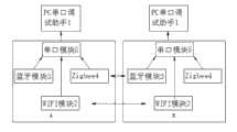
图1为本实用新型的结构示意图;Figure 1 is a schematic structural view of the utility model;
图2为本实用新型的电源电路图;Figure 2 is a power circuit diagram of the utility model;
图3-4为本实用新型的电源引脚滤波电路图;Fig. 3-4 is the power supply pin filter circuit diagram of the present utility model;
图5为本实用新型的晶振时钟电路图;Fig. 5 is the crystal oscillator clock circuit diagram of the present utility model;
图6为本实用新型的复位电路图;Fig. 6 is a reset circuit diagram of the present utility model;
图7为本实用新型的仿真写入电路图。Fig. 7 is the simulation writing circuit diagram of the utility model.
具体实施方式Detailed ways
为使本实用新型实现的技术手段、创作特征、达成目的与功效易于明白了解,下面结合具体实施方式,进一步阐述本实用新型。In order to make the technical means, creative features, goals and effects achieved by the utility model easy to understand, the utility model will be further elaborated below in conjunction with specific embodiments.
参照图1-7,本具体实施方式采用以下技术方案:基于多无线传输协议的网关,包括第一主控芯片A、第二主控芯片B和PC串口调节助手1相连,第一主控芯片A与第二主控芯片B相连,第一主控芯片A、第二主控芯片B均与PC串口调节助手1;所述的第一主控芯片A包括WIFI模块2、蓝牙模块3、zigbee4和串口模块5,WIFI模块2、蓝牙模块3、zigbee4均与串口模块5相连,串口模块5与PC串口调节助手1相连。Referring to Figures 1-7, this embodiment adopts the following technical solutions: a gateway based on a multi-wireless transmission protocol, including a first main control chip A, a second main control chip B connected to the PC serial
值得注意的是,所述的第一主控芯片A与第二主控芯片B均采用STM32F107单片机。It should be noted that both the first main control chip A and the second main control chip B are STM32F107 single-chip microcomputers.
值得注意的是,所述的WIFI模块是基于Uart接口的符合WiFi无线网络标准的嵌入式模块,内置无线网络协议IEEE802.11 协议栈以及 TCP/IP 协议栈,能实现用户串口数据到无线网络之间的转换。通过 Uart-Wifi 模块,传统的串口设备也能轻松接入无线网络。It is worth noting that the WIFI module is an embedded module based on the Uart interface that conforms to the WiFi wireless network standard, and has a built-in wireless network protocol IEEE802. conversion between. Through the Uart-Wifi module, traditional serial devices can also easily access the wireless network.
此外,所述的第一主控芯片A最小系统电路包括电源电路、复位电路、外部时钟电路、晶振电路和写入电路。In addition, the minimum system circuit of the first main control chip A includes a power supply circuit, a reset circuit, an external clock circuit, a crystal oscillator circuit and a writing circuit.
电源电路如图2所示,电路中,引脚6的VBAT为电池,引脚22的VDDA为外部芯片电源,VDD_1~5为外部电源,供给3.3V,VSSA接地。The power supply circuit is shown in Figure 2. In the circuit, VBAT on
电源引脚滤波电路如图3和图4所示。图3中在芯片的电源引脚和地引脚之间连接5个滤波电容,用来滤除电源的毛刺。图4中使用电感来滤除电源中的交流信号,并使用一大一小两个电容来分别滤除电源中的低频噪声和高频噪声。VDDA是经滤波后得到的,VSSA是经滤波后的电感所得到的。减少引线,可增加输入电流大小,Vref为参考电压,电感的作用是通直流阻交流,电容的作用是进行滤波,在参考电压之间增加0.1uF和10uF的滤波电容,其中小电容可以虑高频噪声干扰,大电容可以虑低频噪声干扰。The power supply pin filter circuit is shown in Figure 3 and Figure 4. In Figure 3, 5 filter capacitors are connected between the power supply pin and the ground pin of the chip to filter out the burrs of the power supply. In Figure 4, an inductor is used to filter out the AC signal in the power supply, and two capacitors, one large and one small, are used to filter out the low-frequency noise and high-frequency noise in the power supply respectively. VDDA is obtained after filtering, and VSSA is obtained by filtering the inductor. Reducing the lead wire can increase the input current, Vref is the reference voltage, the function of the inductor is to pass through the DC resistance, and the function of the capacitor is to filter. Add a filter capacitor of 0.1uF and 10uF between the reference voltages, and the small capacitor can be considered high. High-frequency noise interference, large capacitors can consider low-frequency noise interference.
外部时钟电路在单片机系统里,晶振的作用很大,它结合单片机内部的电路,产生单片机运行时需要的时钟频率,单片机的一切指令的执行都是建立在这个基础上的,晶振提供的时钟频率越高,那单片机运行的速度就越快。晶振分为有源晶振和无源晶振两种,本系统中使用的是无源晶振,晶振时钟电路如图5所示。本系统使用的是无源晶振是25MHz的晶振,外加两个电容,大小为20pF,电容大小由芯片手册中指定,输入信号经OSC IN进入,经X1无源晶振,最后输出的信号依然为25MHz,由此产生反馈。External clock circuit In the single-chip microcomputer system, the crystal oscillator plays a very important role. It combines the internal circuit of the single-chip microcomputer to generate the clock frequency required for the operation of the single-chip microcomputer. The execution of all instructions of the single-chip microcomputer is based on this. The clock frequency provided by the crystal oscillator The higher the value, the faster the MCU will run. There are two types of crystal oscillators: active crystal oscillator and passive crystal oscillator. The passive crystal oscillator is used in this system. The crystal oscillator clock circuit is shown in Figure 5. This system uses a passive crystal oscillator, which is a 25MHz crystal oscillator, plus two capacitors with a size of 20pF. The capacitor size is specified in the chip manual. The input signal enters through OSC IN, passes through X1 passive crystal oscillator, and the final output signal is still 25MHz. , resulting in feedback.
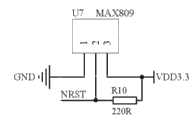
复位电路中使用MAX809复位管理芯片,MAX809为低电平复位管理芯片。用于监控微控制器和其他逻辑系统的电源电压。它可以在上电、掉电和节点情况下向微控制器提空复位信号,当电源电压低于预设的门槛电压时,器件会发出复位信号,直到在一段时间内电源电压又恢复到高于门槛电压为止。MAX809有低电平有效的复位输出,典型值是17uA的低电源电流使MAX809能理想的用于便携式、电池供电的设备。它使用3管脚的SOT23封装。The MAX809 reset management chip is used in the reset circuit, and the MAX809 is a low-level reset management chip. Used to monitor supply voltages for microcontrollers and other logic systems. It can provide a reset signal to the microcontroller under power-on, power-off and node conditions. When the power supply voltage is lower than the preset threshold voltage, the device will issue a reset signal until the power supply voltage returns to high within a period of time. up to the threshold voltage. The MAX809 has an active-low reset output, typically 17uA. The low supply current makes the MAX809 ideal for portable, battery-powered devices. It uses a 3-pin SOT23 package.
复位电路如图6所示。NRST芯片为复位引脚,平常都为高电平,在复位电路中,都会不断监测3号引脚的电压值,当3号引脚的电压值低于2.3V的时候,2号引脚会产生低电平,以此来给主控芯片STM32复位。The reset circuit is shown in Figure 6. The NRST chip is a reset pin, which is usually at a high level. In the reset circuit, the voltage value of the No. 3 pin will be continuously monitored. When the voltage value of the No. 3 pin is lower than 2.3V, the No. 2 pin will be Generate a low level to reset the main control chip STM32.
仿真写入电路如图7所示。仿真写入电路有两种写入方式,分别为JTAG和SWD。JTAG也是一种国际标准测试协议,主要用于芯片内部测试。现在多数的高级器件都支持JTAG协议,如DSP、FPGA器件等。标准的JTAG接口是4线:TMS、TCK、TDI、TDO,分别为模式选择、时钟、数据输入和数据输出线。 相关JTAG引脚的定义为:TCK为测试时钟输入;TDI为测试数据输入,数据通过TDI引脚输入JTAG接口;TDO为测试数据输出,数据通过TDO引脚从JTAG接口输出;TMS为测试模式选择,TMS用来设置JTAG接口处于某种特定的测试模式;TRST为测试复位,输入引脚,低电平有效。The simulation write circuit is shown in Figure 7. There are two writing methods for the simulation writing circuit, namely JTAG and SWD. JTAG is also an international standard test protocol, mainly used for chip internal testing. Now most advanced devices support JTAG protocol, such as DSP, FPGA devices and so on. The standard JTAG interface is 4 lines: TMS, TCK, TDI, TDO, which are mode selection, clock, data input and data output lines respectively. The definition of the relevant JTAG pins is: TCK is the test clock input; TDI is the test data input, and the data is input to the JTAG interface through the TDI pin; TDO is the test data output, and the data is output from the JTAG interface through the TDO pin; TMS is the test mode selection , TMS is used to set the JTAG interface in a specific test mode; TRST is the test reset, input pin, active low.
SWD模式比JTAG在高速模式下面更加可靠。在大数据量的情况下面JTAG下载程序会失败,但是SWD发生的几率会小很多。当GPIO刚好缺一个的时候,可以使用SWD仿真,这种模式支持更少的引脚。当板子体积有限的时候推荐使用SWD模式,它需要的引脚少,当然需要的PCB空间就小了。所以一般用SWD模式更好一些。SWD mode is more reliable than JTAG in high-speed mode. In the case of a large amount of data, the JTAG download program will fail, but the chance of SWD will be much smaller. When the GPIO is just missing one, you can use SWD emulation, which supports fewer pins. It is recommended to use the SWD mode when the board size is limited, it requires fewer pins, and of course requires less PCB space. So it is generally better to use SWD mode.
本具体实施方式STM32F107单片机有如下特点:ARM公司的高性能”Cortex-M3”内核,1.25DMips/MHz,而ARM7TDMI只有0.95DMips/MHz;一流的外设,1μs的双12位ADC,4兆位/秒的UART,18兆位/秒的SPI,18MHz的I/O翻转速度;低功耗,在72MHz时消耗36mA(所有外设处于工作状态),待机时下降到2μA;最大的集成度,复位电路、低电压检测、调压器、精确的RC振荡器等;简单的结构和易用的工具。This specific implementation mode STM32F107 single-chip microcomputer has the following characteristics: ARM's high-performance "Cortex-M3" core, 1.25DMips/MHz, while ARM7TDMI only has 0.95DMips/MHz; first-class peripherals, 1μs dual 12-bit ADC, 4 megabits /sec UART, 18 Mbit/sec SPI, 18MHz I/O flip speed; low power consumption, consuming 36mA at 72MHz (all peripherals are in working state), down to 2μA in standby; maximum integration, Reset circuit, low voltage detection, voltage regulator, accurate RC oscillator, etc.; simple structure and easy-to-use tools.
本具体实施方式可以克服传统网关单一传输协议的缺陷,网络内的wifi模块,蓝牙模块,GPRS模块,3G模块与Zigbee 模块可以实现数据的自由传输。This specific embodiment can overcome the defect of the single transmission protocol of the traditional gateway, and the wifi module, bluetooth module, GPRS module, 3G module and Zigbee module in the network can realize the free transmission of data.
以上显示和描述了本实用新型的基本原理和主要特征和本实用新型的优点。本行业的技术人员应该了解,本实用新型不受上述实施例的限制,上述实施例和说明书中描述的只是说明本实用新型的原理,在不脱离本实用新型精神和范围的前提下,本实用新型还会有各种变化和改进,这些变化和改进都落入要求保护的本实用新型范围内。本实用新型要求保护范围由所附的权利要求书及其等效物界定。The basic principles and main features of the present utility model and the advantages of the present utility model have been shown and described above. Those skilled in the art should understand that the utility model is not limited by the above-mentioned embodiments. The above-mentioned embodiments and descriptions only illustrate the principle of the utility model. Without departing from the spirit and scope of the utility model, the utility model The new model also has various changes and improvements, and these changes and improvements all fall within the scope of the claimed utility model. The scope of protection required by the utility model is defined by the appended claims and their equivalents.
Claims (4)
Priority Applications (1)
| Application Number | Priority Date | Filing Date | Title |
|---|---|---|---|
| CN201320571921.4UCN203446038U (en) | 2013-09-16 | 2013-09-16 | Multiple-wireless transmission protocol-based gateway |
Applications Claiming Priority (1)
| Application Number | Priority Date | Filing Date | Title |
|---|---|---|---|
| CN201320571921.4UCN203446038U (en) | 2013-09-16 | 2013-09-16 | Multiple-wireless transmission protocol-based gateway |
Publications (1)
| Publication Number | Publication Date |
|---|---|
| CN203446038Utrue CN203446038U (en) | 2014-02-19 |
Family
ID=50097046
Family Applications (1)
| Application Number | Title | Priority Date | Filing Date |
|---|---|---|---|
| CN201320571921.4UExpired - Fee RelatedCN203446038U (en) | 2013-09-16 | 2013-09-16 | Multiple-wireless transmission protocol-based gateway |
Country Status (1)
| Country | Link |
|---|---|
| CN (1) | CN203446038U (en) |
Cited By (2)
| Publication number | Priority date | Publication date | Assignee | Title |
|---|---|---|---|---|
| CN103458537A (en)* | 2013-09-16 | 2013-12-18 | 金陵科技学院 | Gateway based on multiple wireless transport protocols |
| CN106909206A (en)* | 2017-04-18 | 2017-06-30 | 湖北科技学院 | A kind of high in the clouds penetrating type serial server |
- 2013
- 2013-09-16CNCN201320571921.4Upatent/CN203446038U/ennot_activeExpired - Fee Related
Cited By (2)
| Publication number | Priority date | Publication date | Assignee | Title |
|---|---|---|---|---|
| CN103458537A (en)* | 2013-09-16 | 2013-12-18 | 金陵科技学院 | Gateway based on multiple wireless transport protocols |
| CN106909206A (en)* | 2017-04-18 | 2017-06-30 | 湖北科技学院 | A kind of high in the clouds penetrating type serial server |
Similar Documents
| Publication | Publication Date | Title |
|---|---|---|
| CN103458537A (en) | Gateway based on multiple wireless transport protocols | |
| CN105634934A (en) | WSN gateway supporting multiple frequency bands and multiple communication modes | |
| CN102938897B (en) | Wireless charging node capable of monitoring signal strength in real time | |
| CN109470301A (en) | Parameter monitoring system and monitoring method for substation resisting strong electromagnetic field interference | |
| CN205541394U (en) | Greenhouse environmental monitoring system based on wireless sensor network | |
| CN203446038U (en) | Multiple-wireless transmission protocol-based gateway | |
| CN105226828A (en) | Based on the photovoltaic microgrid system of Internet of Things sensing technology | |
| CN207457464U (en) | A kind of accumulator wireless monitor system based on technology of Internet of things | |
| CN206294172U (en) | Bandwidth carrier debugging apparatus based on power line communication | |
| CN204556022U (en) | A kind of temperature/humiditydetection detection system based on ZigBee | |
| CN206807400U (en) | A kind of monitoring device of distributed photovoltaic point | |
| CN104284403A (en) | A Design Method for Low Power Consumption Nodes in Wireless Sensor Networks | |
| CN108973900A (en) | Automobile mounted terminal device | |
| CN202257906U (en) | Multifunctional low-power consumption intelligent node of wireless sensor network | |
| CN209659346U (en) | A/D capture card based on NB-iot technology | |
| CN208572452U (en) | A kind of super low-power consumption wifi- serial ports transparent transmission conversion module | |
| CN203397130U (en) | Circuit of on-off switching device applied to electronic equipment | |
| CN201904810U (en) | Field bus protocol converter based on wireless technology | |
| CN205429874U (en) | Photovoltaic microgrid system based on thing networking sensing technology | |
| CN206313545U (en) | A power supply system for an active electromagnetic stylus | |
| CN107037751A (en) | A kind of electric power monitoring system based on CAN | |
| CN103167039B (en) | A kind of development platform towards polymorphic type ZigBee node | |
| CN210807299U (en) | A security alarm device for substation dispatching data network | |
| CN210428433U (en) | Multifunctional interface converter based on Internet of things | |
| CN205404677U (en) | Electricity inspection terminal with real -time clock |
Legal Events
| Date | Code | Title | Description |
|---|---|---|---|
| C14 | Grant of patent or utility model | ||
| GR01 | Patent grant | ||
| CF01 | Termination of patent right due to non-payment of annual fee | ||
| CF01 | Termination of patent right due to non-payment of annual fee | Granted publication date:20140219 Termination date:20160916 |