Movatterモバイル変換


[0]ホーム

URL:


CN203261508U - Constant-power LED power supply circuit - Google Patents

Constant-power LED power supply circuit
Download PDF

Info

Publication number
CN203261508U
CN203261508UCN 201320179274CN201320179274UCN203261508UCN 203261508 UCN203261508 UCN 203261508UCN 201320179274CN201320179274CN 201320179274CN 201320179274 UCN201320179274 UCN 201320179274UCN 203261508 UCN203261508 UCN 203261508U
Authority
CN
China
Prior art keywords
resistor
capacitor
pin
power supply
circuit
Prior art date
Legal status (The legal status is an assumption and is not a legal conclusion. Google has not performed a legal analysis and makes no representation as to the accuracy of the status listed.)
Expired - Fee Related
Application number
CN 201320179274
Other languages
Chinese (zh)
Inventor
杜鹏英
任国海
姚立海
江皓
Current Assignee (The listed assignees may be inaccurate. Google has not performed a legal analysis and makes no representation or warranty as to the accuracy of the list.)
Hangzhou City University
Original Assignee
Zhejiang University City College ZUCC
Priority date (The priority date is an assumption and is not a legal conclusion. Google has not performed a legal analysis and makes no representation as to the accuracy of the date listed.)
Filing date
Publication date
Application filed by Zhejiang University City College ZUCCfiledCriticalZhejiang University City College ZUCC
Priority to CN 201320179274priorityCriticalpatent/CN203261508U/en
Application grantedgrantedCritical
Publication of CN203261508UpublicationCriticalpatent/CN203261508U/en
Anticipated expirationlegal-statusCritical
Expired - Fee Relatedlegal-statusCriticalCurrent

Links

Images

Landscapes

Abstract

Translated fromChinese

本实用新型公开一种恒功率LED电源电路。目前LED电源多用恒压或恒流方式,虽总功率相同但需定向配置,增加成本且不方便。该电路包括输入电源整流滤波电路、开关电源电路、电压反馈电路、电流反馈电路、模拟乘法器电路、LED负载。输入电源整流滤波电路输入端接220V电压、输出端与开关电源电路一个输入端连接,开关电源电路一个输出端与电压反馈电路输入端连接、另一个输出端与电流反馈电路输入端连接、又一个输出端与LED负载输入端连接,模拟乘法器电路一个输入端与电压反馈电路输出端连接、另一个输入端与电流反馈电路输出端连接、输出端与开关电源电路另一个输入端连接。该电路串并联不同连接下LED负载供电恒功率。

Figure 201320179274

The utility model discloses a constant power LED power supply circuit. At present, LED power supply mostly uses constant voltage or constant current mode. Although the total power is the same, it needs to be configured in a specific way, which increases the cost and is inconvenient. The circuit includes an input power rectifying and filtering circuit, a switching power supply circuit, a voltage feedback circuit, a current feedback circuit, an analog multiplier circuit, and an LED load. The input terminal of the input power rectification filter circuit is connected to 220V voltage, the output terminal is connected to one input terminal of the switching power supply circuit, one output terminal of the switching power supply circuit is connected to the input terminal of the voltage feedback circuit, the other output terminal is connected to the input terminal of the current feedback circuit, and another The output terminal is connected to the LED load input terminal, one input terminal of the analog multiplier circuit is connected to the output terminal of the voltage feedback circuit, the other input terminal is connected to the output terminal of the current feedback circuit, and the output terminal is connected to the other input terminal of the switching power supply circuit. The circuit is connected in series and parallel to supply LED loads with constant power under different connections.

Figure 201320179274

Description

Translated fromChinese
一种恒功率LED电源电路A constant power LED power supply circuit

技术领域technical field

本实用新型属于电源技术和照明领域,具体涉及一种恒功率LED电源电路。The utility model belongs to the field of power supply technology and lighting, in particular to a constant power LED power supply circuit.

背景技术Background technique

在节能减排呼声高涨的今天,LED照明将逐步成为照明技术的发展主流已成为共识。被称之为又一次照明革命的LED固体光源开发应用已成为本世纪重点发展的目标之一,我国的LED产业也进入加速发展的阶段。LED驱动电源是LED产业链发展的保障,LED电源的品质会影响和制约LED产业的发展。研究LED驱动电源对LED产业的应用具有重大意义。对于LED照明应用而言,其标准灯具具有统一的外形尺寸和功率,但内部LED的串并联方式却有多种变化,造成不同厂家生产的同类灯具其驱动电压、电流各不相同。目前的LED驱动电源多采用恒压或恒流方式,因此虽然灯具总功率相同,但驱动电源却需要定向配置而不能像传统电子镇流器那般具有较好的通用性,这不仅推高了LED照明设备的成本,也给实际的应用带来很多不便。Today, with the rising calls for energy saving and emission reduction, it has become a consensus that LED lighting will gradually become the mainstream of lighting technology development. The development and application of LED solid-state light source, which is called another lighting revolution, has become one of the key development goals of this century, and my country's LED industry has also entered a stage of accelerated development. LED driving power supply is the guarantee for the development of LED industry chain, and the quality of LED power supply will affect and restrict the development of LED industry. Research on LED driving power supply is of great significance to the application of LED industry. For LED lighting applications, the standard lamps have uniform dimensions and power, but there are many changes in the series and parallel connection of internal LEDs, resulting in different driving voltages and currents for similar lamps produced by different manufacturers. The current LED drive power supply mostly adopts constant voltage or constant current mode, so although the total power of the lamps is the same, the drive power supply needs to be configured in a directional manner and cannot have good versatility like traditional electronic ballasts, which not only pushes up The cost of LED lighting equipment also brings a lot of inconvenience to practical applications.

发明内容Contents of the invention

本实用新型针对现有技术的不足,提供了一种恒功率LED驱动电源电路。The utility model provides a constant power LED driving power supply circuit aiming at the deficiencies of the prior art.

本实用新型包括输入电源整流滤波电路、开关电源电路、电压反馈电路、电流反馈电路、模拟乘法器电路、LED负载。输入电源整流滤波电路的输入端接220V电压、输出端与开关电源电路的一个输入端信号连接,开关电源电路的一个输出端与电压反馈电路的输入端信号连接,开关电源电路的另一个输出端与电流反馈电路的输入端信号连接,开关电源的又一个输出端与LED负载的输入端信号连接;电压反馈电路的输出端与模拟乘法器电路的一个输入端信号连接,电流反馈电路的输出端与模拟乘法器电路的另一个输入端信号连接,模拟乘法器电路的输出端与开关电源电路的另一个输入端信号连接。The utility model comprises an input power rectifying and filtering circuit, a switching power supply circuit, a voltage feedback circuit, a current feedback circuit, an analog multiplier circuit and an LED load. The input terminal of the input power rectification and filtering circuit is connected to 220V voltage, the output terminal is connected to an input terminal signal of the switching power supply circuit, one output terminal of the switching power supply circuit is connected to the input terminal signal of the voltage feedback circuit, and the other output terminal of the switching power supply circuit It is connected to the input signal of the current feedback circuit, another output terminal of the switching power supply is connected to the input terminal signal of the LED load; the output terminal of the voltage feedback circuit is connected to an input terminal signal of the analog multiplier circuit, and the output terminal of the current feedback circuit It is signal-connected with the other input end of the analog multiplier circuit, and the output end of the analog multiplier circuit is signal-connected with the other input end of the switching power supply circuit.

所述的输入电源整流滤波电路包括熔断器F、整流桥D、共模电感LA、第一电感L1、第二电感L2、第一电容C1、第二电容C2、第三电容C3;熔断器F的一端与220V电压一个输入接口J1连接,另一端与第一电感L1的一端、第一电容C1的一端连接,第一电容C1的另一端和第二电感L2的一端与220V电压另一个输入接口J2连接;第一电感L1的另一端与共模电感LA的第1引脚连接,第二电感L2的另一端与共模电感LA的第2引脚连接;整流桥D由四个二极管构成,第一二极管D1的阳极与第二二极管D2的阴极连接后与共模电感LA的第3引脚、第二电容C2的一端连接,第三二极管D3的阳极与第四二极管D4的阴极连接后与共模电感LA的第4引脚、第三电容C3的一端连接,第二电容C2的另一端和第三电容C3的另一端与220V电压的地线接口J3连接;第二二极管D2的阳极与第四二极管D4的阳极连接后接地,第一二极管D1的阴极与第三二极管D3的阴极连接后作为输入电源整流滤波电路的输出端。The input power rectification filter circuit includes a fuse F, a rectifier bridge D, a common mode inductor LA, a first inductor L1, a second inductor L2, a first capacitor C1, a second capacitor C2, and a third capacitor C3; the fuse F One end of the first capacitor C1 and one end of the second inductor L2 are connected to the other input interface of 220V voltage. J2 connection; the other end of the first inductor L1 is connected to the first pin of the common mode inductor LA, and the other end of the second inductor L2 is connected to the second pin of the common mode inductor LA; the rectifier bridge D is composed of four diodes, the first The anode of the diode D1 is connected to the cathode of the second diode D2 and then connected to the third pin of the common mode inductor LA and one end of the second capacitor C2, and the anode of the third diode D3 is connected to the fourth diode D4 After connecting the cathode of the common mode inductor LA to the fourth pin and one end of the third capacitor C3, the other end of the second capacitor C2 and the other end of the third capacitor C3 are connected to the 220V ground interface J3; the second two The anode of the diode D2 is connected to the anode of the fourth diode D4 and grounded, and the cathode of the first diode D1 is connected to the cathode of the third diode D3 to serve as the output terminal of the input power rectification and filtering circuit.

所述的开关电源电路包括电流脉宽调制器U1、MOSFET管VT、变压器T、第一绕组La、第二绕组Lb、第三绕组Lc、第一电阻R1、第二电阻R2、第三电阻R3、第四电阻R4、第五电阻R5、第六电阻R6、第七电阻R7、第八电阻R8、第九电阻R9、第十电阻R10、第十一电阻R11、第四电容C4、第五电容C5、第六电容C6、第七电容C7、第八电容C8、第九电容C9、第十电容C10、第十一电容C11、第十二电容C12、第十三电容C13、第十四电容C14、第十五电容C15、第十六电容C16、第十七电容C17、第十八电容C18、第十九电容C19、第二十电容C20、第五二极管D5、第六二极管D6、第七二极管D7、第八二极管D8、第九二极管D9、发光二极管D10、第三电感L3、第四电感L4;电流脉宽调制器U1的第1引脚与第四电容C4的一端、第一电阻R1的一端连接后作为开关电源电路的一个反馈输入端V1,第2引脚与第二电阻R2的一端连接,第9引脚与第一电阻R1的另一端、第三电阻R3的一端、第五电容C5的一端连接,第7引脚与第四电阻R4的一端连接,第5引脚与第四电阻R4的另一端、第六电容C6的一端连接,第6引脚与第五电阻R5的一端连接,第8引脚与第七电容C7的正极连接,第13引脚与第15引脚、第六电阻R6的一端、第八电容C8的正极、第三电感L3的一端连接后接电源VCC,第16引脚与第二电阻R2的另一端、第九电容C9的一端连接,第11引脚与第七电阻R7的一端连接,第10引脚与第十电容C10的一端、第八电阻R8的一端连接,第12引脚与第九电阻R9的一端、第十电容C10的另一端、第八电容C8的负极、第九电容C9的另一端、第七电容C7的负极、第五电阻R5的另一端、第六电容C6的另一端、第五电容C5的另一端、第十一电容C11的一端连接后接地,其他引脚均架空;第三电感L3的另一端与第五二极管D5的阴极、第十二电容C12的一端连接;变压器由三个绕阻构成,第一绕阻La的一端与第六二极管D6的阳极、第十电阻R10的一端、第十三电容C13的一端、第六电阻R6的另一端、第十一电容C11的另一端连接后与输入电源整流滤波电路的输出端连接,第一绕阻La的另一端与第七二极管D7的阳极、MOSFET管VT的漏极连接,第二绕阻Lb的一端与第八二极管D8的阳极连接,第二绕阻Lb的另一端与第十四电容C14的负极、第十五电容C15的一端、第十六电容C16的负极、第十七电容C17的负极、第十八电容C18的一端、第十九电容C19的一端连接后作为开关电源电路的一个输出接口J4连接,第三绕阻Lc的一端与第九二极管D9的阳极连接,第三绕阻Lc的另一端与第二十电容C20的负极、第十二电容C12的另一端、第十九电容C19的另一端、发光二极管D10的阴极连接后接地;MOSFET管VT的栅极与第七电阻R7的另一端连接,源极与第八电阻R8的另一端、第九电阻R9的另一端连接后作为开关电源电路的第一输出端V2;第八二极管D8的阴极与第十四电容C14的正极、第十五电容C15的一端、第十六电容C16的正极、第四电感L4的一端连接;第四电感L4的另一端与第十七电容C17的正极、第十八电容C18的另一端连接后作为开关电源电路的一个输出接口J5连接;第九二极管D9的阴极与第二十电容C20的正极、第五二极管D5的阳极、第十一电阻R11的一端连接后作为开关电源电路的第二输出端V3;第十一电阻R11的另一端与发光二极管D10的阳极连接。所述的电流脉宽调制器U1的型号为SG3525A。The switching power supply circuit includes a current pulse width modulator U1, a MOSFET tube VT, a transformer T, a first winding La, a second winding Lb, a third winding Lc, a first resistor R1, a second resistor R2, and a third resistor R3 , the fourth resistor R4, the fifth resistor R5, the sixth resistor R6, the seventh resistor R7, the eighth resistor R8, the ninth resistor R9, the tenth resistor R10, the eleventh resistor R11, the fourth capacitor C4, the fifth capacitor C5, sixth capacitor C6, seventh capacitor C7, eighth capacitor C8, ninth capacitor C9, tenth capacitor C10, eleventh capacitor C11, twelfth capacitor C12, thirteenth capacitor C13, fourteenth capacitor C14 , the fifteenth capacitor C15, the sixteenth capacitor C16, the seventeenth capacitor C17, the eighteenth capacitor C18, the nineteenth capacitor C19, the twentieth capacitor C20, the fifth diode D5, and the sixth diode D6 , the seventh diode D7, the eighth diode D8, the ninth diode D9, the light emitting diode D10, the third inductor L3, the fourth inductor L4; the first pin and the fourth pin of the current pulse width modulator U1 One end of the capacitor C4 and one end of the first resistor R1 are connected to serve as a feedback input terminal V1 of the switching power supply circuit, the second pin is connected to one end of the second resistor R2, the ninth pin is connected to the other end of the first resistor R1, One end of the third resistor R3 is connected to one end of the fifth capacitor C5, the seventh pin is connected to one end of the fourth resistor R4, the fifth pin is connected to the other end of the fourth resistor R4, and one end of the sixth capacitor C6, and the fifth pin is connected to the other end of the fourth resistor R4 and one end of the sixth capacitor C6. The 6th pin is connected to one end of the fifth resistor R5, the 8th pin is connected to the positive pole of the seventh capacitor C7, the 13th pin is connected to the 15th pin, one end of the sixth resistor R6, the positive pole of the eighth capacitor C8, the One end of the three inductance L3 is connected to the power supply VCC, the 16th pin is connected to the other end of the second resistor R2 and one end of the ninth capacitor C9, the 11th pin is connected to one end of the seventh resistor R7, and the 10th pin is connected to the One end of the tenth capacitor C10 and one end of the eighth resistor R8 are connected, the 12th pin is connected to one end of the ninth resistor R9, the other end of the tenth capacitor C10, the negative pole of the eighth capacitor C8, the other end of the ninth capacitor C9, The negative pole of the seventh capacitor C7, the other end of the fifth resistor R5, the other end of the sixth capacitor C6, the other end of the fifth capacitor C5, and one end of the eleventh capacitor C11 are connected to ground, and the other pins are all overhead; the third The other end of the inductance L3 is connected to the cathode of the fifth diode D5 and one end of the twelfth capacitor C12; the transformer is composed of three windings, one end of the first winding La is connected to the anode of the sixth diode D6, the first end of the twelfth capacitor C12 One end of the tenth resistor R10, one end of the thirteenth capacitor C13, the other end of the sixth resistor R6, and the other end of the eleventh capacitor C11 are connected to the output end of the input power rectification filter circuit, and the other end of the first winding La One end is connected to the anode of the seventh diode D7 and the drain of the MOSFET tube VT, one end of the second winding Lb is connected to the anode of the eighth diode D8, and the other end of the second winding Lb is connected to the fourteenth capacitor The negative pole of C14, the fifteenth capacitor C15 One end of the sixteenth capacitor C16, the negative electrode of the seventeenth capacitor C17, one end of the eighteenth capacitor C18, and one end of the nineteenth capacitor C19 are connected as an output interface J4 of the switching power supply circuit, and the third winding One end of the resistance Lc is connected to the anode of the ninth diode D9, the other end of the third winding Lc is connected to the negative pole of the twentieth capacitor C20, the other end of the twelfth capacitor C12, the other end of the nineteenth capacitor C19, The cathode of the light-emitting diode D10 is connected to the ground; the gate of the MOSFET VT is connected to the other end of the seventh resistor R7, and the source is connected to the other end of the eighth resistor R8 and the other end of the ninth resistor R9 to serve as a switching power supply circuit. The first output terminal V2; the cathode of the eighth diode D8 is connected to the positive pole of the fourteenth capacitor C14, one end of the fifteenth capacitor C15, the positive pole of the sixteenth capacitor C16, and one end of the fourth inductor L4; the fourth inductor The other end of L4 is connected to the positive pole of the seventeenth capacitor C17 and the other end of the eighteenth capacitor C18 as an output interface J5 of the switching power supply circuit; the cathode of the ninth diode D9 is connected to the positive pole of the twentieth capacitor C20 , the anode of the fifth diode D5 and one end of the eleventh resistor R11 are connected to serve as the second output terminal V3 of the switching power supply circuit; the other end of the eleventh resistor R11 is connected to the anode of the light emitting diode D10. The model of the current pulse width modulator U1 is SG3525A.

所述的开关电源电路的两个输出接口J4和J5 与LED负载的输入接口连接。所述的LED负载为现有LED照明装置。The two output interfaces J4 and J5 of the switching power supply circuit are connected to the input interface of the LED load. The LED load is an existing LED lighting device.

所述的电压反馈电路包括第十二电阻R12、第十三电阻R13、滑动变阻Rx;第十二电阻R12的一端与滑动变阻Rx的一端连接、另一端接地,滑动变阻Rx的另一端与第十三电阻R13的一端连接、滑动端作为电压反馈电路的输出端,第十三电阻R13的另一端与开关电源电路的第二输出端V3连接。The voltage feedback circuit includes a twelfth resistor R12, a thirteenth resistor R13, and a sliding rheostat Rx; one end of the twelfth resistor R12 is connected to one end of the sliding rheostat Rx, the other end is grounded, and the other end of the sliding rheostat Rx One end is connected to one end of the thirteenth resistor R13, the sliding end is used as the output end of the voltage feedback circuit, and the other end of the thirteenth resistor R13 is connected to the second output end V3 of the switching power supply circuit.

所述的电流反馈电路包括放大器U2、第十四电阻R14、第十五电阻R15、第十六电阻R16、第十七电阻R17、第十八电阻R18、第十九电阻R19、第二十电阻R20、第二十一电容C21、第二十二电容C22、第二十三电容C23、第五电感L5;放大器U2的第1引脚与第十四电阻R14的一端、第十五电阻R15的一端、第二十一电容C21的一端连接,第2引脚与第十六电阻R16的一端连接,第3引脚与第十五电阻R15的另一端、第二十一电容C21的另一端、第十七电阻R17的一端连接,第4引脚接地,第5引脚与第十四电阻R14的另一端连接,第6引脚与第十八电阻R18的一端、第十九电阻R19的一端、第二十二电容C22的一端连接,第7引脚与第十八电阻R18的另一端、第二十二电容C22的另一端连接后作为电流反馈电路的输出端,第8引脚与电源VCC连接;第十六电阻R16的另一端与第二十电阻R20的一端、第二十三电容C23的一端、第五电感L5的一端连接;第二十电阻R20的另一端与第二十三电容C23的另一端连接后接地;第十九电阻R19的另一端、第十七电阻R17的另一端均接地;第五电感L5的另一端与开关电源电路的第一输出端V2连接。所述的放大器U2的型号为LM358。The current feedback circuit includes amplifier U2, fourteenth resistor R14, fifteenth resistor R15, sixteenth resistor R16, seventeenth resistor R17, eighteenth resistor R18, nineteenth resistor R19, twentieth resistor R20, the twenty-first capacitor C21, the twenty-second capacitor C22, the twenty-third capacitor C23, the fifth inductance L5; the first pin of the amplifier U2 and one end of the fourteenth resistor R14, and one end of the fifteenth resistor R15 One end, one end of the twenty-first capacitor C21 is connected, the second pin is connected to one end of the sixteenth resistor R16, the third pin is connected to the other end of the fifteenth resistor R15, the other end of the twenty-first capacitor C21, One end of the seventeenth resistor R17 is connected, the fourth pin is grounded, the fifth pin is connected to the other end of the fourteenth resistor R14, the sixth pin is connected to one end of the eighteenth resistor R18, and one end of the nineteenth resistor R19 , One end of the twenty-second capacitor C22 is connected, the seventh pin is connected to the other end of the eighteenth resistor R18, and the other end of the twenty-second capacitor C22 is used as the output end of the current feedback circuit, and the eighth pin is connected to the power supply VCC is connected; the other end of the sixteenth resistor R16 is connected to one end of the twentieth resistor R20, one end of the twenty-third capacitor C23, and one end of the fifth inductor L5; the other end of the twentieth resistor R20 is connected to the twenty-third resistor R20. The other end of the capacitor C23 is connected to ground; the other end of the nineteenth resistor R19 and the seventeenth resistor R17 are grounded; the other end of the fifth inductor L5 is connected to the first output end V2 of the switching power supply circuit. The model of the amplifier U2 is LM358.

所述的模拟乘法器电路包括模拟乘法器U3、第二十一电阻R21、第二十二电阻R22、第二十三电阻R23;模拟乘法器U3的第1引脚与电流反馈电路的输出端连接,第2引脚与第4引脚、第5引脚、第二十一电阻R21的一端连接后接地,第3引脚与电压反馈电路的输出端连接,第6引脚与第二十一电阻R21的另一端、第二十二电阻R22的一端、第二十三电阻R23的一端连接,第7引脚与第二十三电阻R23的另一端连接,第8引脚与电源VCC连接;第二十二电阻R22的另一端与开关电源电路的一个反馈输入端V1连接。所述的模拟乘法器U3的型号为AD633。Described analog multiplier circuit comprises analog multiplier U3, twenty-first resistor R21, twenty-second resistor R22, twenty-third resistor R23; the first pin of analog multiplier U3 and the output end of current feedback circuit connection, the 2nd pin is connected to the 4th pin, the 5th pin, and one end of the 21st resistor R21 and then grounded, the 3rd pin is connected to the output end of the voltage feedback circuit, the 6th pin is connected to the 20th The other end of the first resistor R21, one end of the twenty-second resistor R22, and one end of the twenty-third resistor R23 are connected, the seventh pin is connected to the other end of the twenty-third resistor R23, and the eighth pin is connected to the power supply VCC ; The other end of the twenty-second resistor R22 is connected to a feedback input terminal V1 of the switching power supply circuit. The model of the analog multiplier U3 is AD633.

本实用新型有益效果是:通过本实用新型可以实现恒功率情况下串并联不同连接情况的LED负载组的供电都能够恒功率。本实用新型改变了在传统的不同连接方式下,电源不能通用的局限性,有利于LED负载组的统一标配,简化LED负载组电源的配备,有效促进LED负载组的广泛应用。The beneficial effect of the utility model is that: the utility model can realize the power supply of the LED load groups connected in series and parallel with different connection conditions under the condition of constant power, and the power supply can be constant. The utility model changes the limitation that the power supply cannot be used universally in different traditional connection modes, is beneficial to the unified standard configuration of the LED load group, simplifies the configuration of the power supply of the LED load group, and effectively promotes the wide application of the LED load group.

附图说明Description of drawings

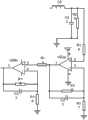
图1为本实用新型的系统构成示意图;Fig. 1 is the system composition schematic diagram of the present utility model;

图2为输入电源整流滤波电路的电路图;Fig. 2 is the circuit diagram of input power supply rectification filter circuit;

图3为开关电源的电路图; Fig. 3 is the circuit diagram of switching power supply;

图4为电压反馈电路的电路图;Fig. 4 is the circuit diagram of voltage feedback circuit;

图5为电流反馈电路的电路图;Fig. 5 is the circuit diagram of current feedback circuit;

图6为模拟乘法器电路的电路图。FIG. 6 is a circuit diagram of an analog multiplier circuit.

具体实施方式Detailed ways

下面结合附图对本实用新型作进一步的分析。Below in conjunction with accompanying drawing, the utility model is further analyzed.

如图1所示,本实用新型包括输入电源整流滤波电路1、开关电源电路2、电压反馈电路3、电流反馈电路4、模拟乘法器电路5、LED负载6。输入电源整流滤波电路1的输入端接220V电压、输出端与开关电源电路2的一个输入端信号连接,开关电源电路2的一个输出端与电压反馈电路3的输入端信号连接,开关电源电路2的另一个输出端与电流反馈电路4的输入端信号连接,开关电源的又一个输出端与LED负载6的输入端信号连接;电压反馈电路3的输出端与模拟乘法器电路5的一个输入端信号连接,电流反馈电路4的输出端与模拟乘法器电路5的另一个输入端信号连接,模拟乘法器电路5的输出端与开关电源电路2的另一个输入端信号连接。As shown in FIG. 1 , the utility model includes an input power rectifying andfiltering circuit 1 , a switchingpower supply circuit 2 , avoltage feedback circuit 3 , acurrent feedback circuit 4 , ananalog multiplier circuit 5 , and anLED load 6 . The input terminal of the input power rectification andfiltering circuit 1 is connected to 220V voltage, the output terminal is connected with an input terminal signal of the switchingpower supply circuit 2, and one output terminal of the switchingpower supply circuit 2 is connected with the input terminal signal of thevoltage feedback circuit 3, and the switchingpower supply circuit 2 The other output terminal of the switching power supply is connected to the input terminal signal of thecurrent feedback circuit 4, and another output terminal of the switching power supply is connected to the input terminal signal of theLED load 6; the output terminal of thevoltage feedback circuit 3 is connected to an input terminal of theanalog multiplier circuit 5 Signal connection, the output end of thecurrent feedback circuit 4 is connected to the other input end of theanalog multiplier circuit 5 , and the output end of theanalog multiplier circuit 5 is connected to the other input end of the switchingpower supply circuit 2 .

如图2所示,输入电源整流滤波电路1包括熔断器F、整流桥D、共模电感LA、第一电感L1、第二电感L2、第一电容C1、第二电容C2、第三电容C3;熔断器F的一端与220V电压一个输入接口J1连接,另一端与第一电感L1的一端、第一电容C1的一端连接,第一电容C1的另一端和第二电感L2的一端与220V电压另一个输入接口J2连接;第一电感L1的另一端与共模电感LA的第1引脚连接,第二电感L2的另一端与共模电感LA的第2引脚连接;整流桥D由四个二极管构成,第一二极管D1的阳极与第二二极管D2的阴极连接后与共模电感LA的第3引脚、第二电容C2的一端连接,第三二极管D3的阳极与第四二极管D4的阴极连接后与共模电感LA的第4引脚、第三电容C3的一端连接,第二电容C2的另一端和第三电容C3的另一端与220V电压的地线接口J3连接;第二二极管D2的阳极与第四二极管D4的阳极连接后接地,第一二极管D1的阴极与第三二极管D3的阴极连接后作为输入电源整流滤波电路1的输出端。As shown in Figure 2, the input powerrectification filter circuit 1 includes a fuse F, a rectifier bridge D, a common mode inductor LA, a first inductor L1, a second inductor L2, a first capacitor C1, a second capacitor C2, and a third capacitor C3 ; One end of the fuse F is connected to an input interface J1 of 220V voltage, the other end is connected to one end of the first inductance L1 and one end of the first capacitor C1, and the other end of the first capacitor C1 and one end of the second inductance L2 are connected to the 220V voltage The other input interface J2 is connected; the other end of the first inductor L1 is connected to the first pin of the common mode inductor LA, and the other end of the second inductor L2 is connected to the second pin of the common mode inductor LA; the rectifier bridge D is composed of four diodes Composition, the anode of the first diode D1 is connected to the cathode of the second diode D2 and then connected to the third pin of the common mode inductor LA and one end of the second capacitor C2, and the anode of the third diode D3 is connected to the fourth The cathode of the diode D4 is connected to the fourth pin of the common mode inductor LA and one end of the third capacitor C3, and the other end of the second capacitor C2 and the other end of the third capacitor C3 are connected to the 220V ground wire interface J3 ; The anode of the second diode D2 is connected to the anode of the fourth diode D4 and grounded, and the cathode of the first diode D1 is connected to the cathode of the third diode D3 as the output of the input powerrectification filter circuit 1 end.

如图3所示,开关电源电路2包括电流脉宽调制器U1、MOSFET管VT、变压器T、第一绕组La、第二绕组Lb、第三绕组Lc、第一电阻R1、第二电阻R2、第三电阻R3、第四电阻R4、第五电阻R5、第六电阻R6、第七电阻R7、第八电阻R8、第九电阻R9、第十电阻R10、第十一电阻R11、第四电容C4、第五电容C5、第六电容C6、第七电容C7、第八电容C8、第九电容C9、第十电容C10、第十一电容C11、第十二电容C12、第十三电容C13、第十四电容C14、第十五电容C15、第十六电容C16、第十七电容C17、第十八电容C18、第十九电容C19、第二十电容C20、第五二极管D5、第六二极管D6、第七二极管D7、第八二极管D8、第九二极管D9、发光二极管D10、第三电感L3、第四电感L4;电流脉宽调制器U1的第1引脚与第四电容C4的一端、第一电阻R1的一端连接后作为开关电源电路2的一个输出端V1,第2引脚与第二电阻R2的一端连接,第9引脚与第一电阻R1的另一端、第三电阻R3的一端、第五电容C5的一端连接,第7引脚与第四电阻R4的一端连接,第5引脚与第四电阻R4的另一端、第六电容C6的一端连接,第6引脚与第五电阻R5的一端连接,第8引脚与第七电容C7的正极连接,第13引脚与第15引脚、第六电阻R6的一端、第八电容C8的正极、第三电感L3的一端连接后接电源VCC,第16引脚与第二电阻R2的另一端、第九电容C9的一端连接,第11引脚与第七电阻R7的一端连接,第10引脚与第十电容C10的一端、第八电阻R8的一端连接,第12引脚与第九电阻R9的一端、第十电容C10的另一端、第八电容C8的负极、第九电容C9的另一端、第七电容C7的负极、第五电阻R5的另一端、第六电容C6的另一端、第五电容C5的另一端、第十一电容C11的一端连接后接地,其他引脚均架空;第三电感L3的另一端与第五二极管D5的阴极、第十二电容C12的一端连接;变压器由三个绕阻构成,第一绕阻La的一端与第六二极管D6的阳极、第十电阻R10的一端、第十三电容C13的一端、第六电阻R6的另一端、第十一电容C11的另一端连接后与输入电源整流滤波电路1的输出端连接,第一绕阻La的另一端与第七二极管D7的阳极、MOSFET管VT的漏极连接,第二绕阻Lb的一端与第八二极管D8的阳极连接,第二绕阻Lb的另一端与第十四电容C14的负极、第十五电容C15的一端、第十六电容C16的负极、第十七电容C17的负极、第十八电容C18的一端、第十九电容C19的一端连接后作为开关电源电路2的一个输出接口J4连接,第三绕阻Lc的一端与第九二极管D9的阳极连接,第三绕阻Lc的另一端与第二十电容C20的负极、第十二电容C12的另一端、第十九电容C19的另一端、发光二极管D10的阴极连接后接地;MOSFET管VT的栅极与第七电阻R7的另一端连接,源极与第八电阻R8的另一端、第九电阻R9的另一端连接后作为开关电源电路2的第一输出端V2;第八二极管D8的阴极与第十四电容C14的正极、第十五电容C15的一端、第十六电容C16的正极、第四电感L4的一端连接;第四电感L4的另一端与第十七电容C17的正极、第十八电容C18的另一端连接后作为开关电源电路2的一个输出接口J5连接;第九二极管D9的阴极与第二十电容C20的正极、第五二极管D5的阳极、第十一电阻R11的一端连接后作为开关电源电路2的第二输出端V3;第十一电阻R11的另一端与发光二极管D10的阳极连接。所述的电流脉宽调制器U1的型号为SG3525A。As shown in Figure 3, the switchingpower supply circuit 2 includes a current pulse width modulator U1, a MOSFET tube VT, a transformer T, a first winding La, a second winding Lb, a third winding Lc, a first resistor R1, a second resistor R2, The third resistor R3, the fourth resistor R4, the fifth resistor R5, the sixth resistor R6, the seventh resistor R7, the eighth resistor R8, the ninth resistor R9, the tenth resistor R10, the eleventh resistor R11, the fourth capacitor C4 , the fifth capacitor C5, the sixth capacitor C6, the seventh capacitor C7, the eighth capacitor C8, the ninth capacitor C9, the tenth capacitor C10, the eleventh capacitor C11, the twelfth capacitor C12, the thirteenth capacitor C13, the Fourteenth capacitor C14, fifteenth capacitor C15, sixteenth capacitor C16, seventeenth capacitor C17, eighteenth capacitor C18, nineteenth capacitor C19, twentieth capacitor C20, fifth diode D5, sixth Diode D6, seventh diode D7, eighth diode D8, ninth diode D9, light emitting diode D10, third inductance L3, fourth inductance L4; the first lead of the current pulse width modulator U1 The pin is connected to one end of the fourth capacitor C4 and one end of the first resistor R1 as an output terminal V1 of the switchingpower supply circuit 2, the second pin is connected to one end of the second resistor R2, and the ninth pin is connected to the first resistor R1 The other end of the third resistor R3, one end of the fifth capacitor C5, the seventh pin is connected to one end of the fourth resistor R4, the fifth pin is connected to the other end of the fourth resistor R4, the sixth capacitor C6 One end is connected, the 6th pin is connected to one end of the fifth resistor R5, the 8th pin is connected to the positive pole of the seventh capacitor C7, the 13th pin is connected to the 15th pin, one end of the sixth resistor R6, and the eighth capacitor C8 The positive pole of the third inductor L3 is connected to the power supply VCC, the 16th pin is connected to the other end of the second resistor R2, and one end of the ninth capacitor C9, the 11th pin is connected to one end of the seventh resistor R7, and the Pin 10 is connected to one end of the tenth capacitor C10 and one end of the eighth resistor R8, the 12th pin is connected to one end of the ninth resistor R9, the other end of the tenth capacitor C10, the negative pole of the eighth capacitor C8, and the ninth capacitor C9 The other end of the seventh capacitor C7, the other end of the fifth resistor R5, the other end of the sixth capacitor C6, the other end of the fifth capacitor C5, and one end of the eleventh capacitor C11 are connected to ground, and the other pins are overhead; the other end of the third inductor L3 is connected to the cathode of the fifth diode D5 and one end of the twelfth capacitor C12; the transformer is composed of three windings, and one end of the first winding La is connected to the sixth diode D6 The anode of the anode, one end of the tenth resistor R10, one end of the thirteenth capacitor C13, the other end of the sixth resistor R6, and the other end of the eleventh capacitor C11 are connected to the output end of the input powerrectification filter circuit 1, and the first The other end of the winding La is connected to the anode of the seventh diode D7 and the drain of the MOSFET tube VT, one end of the second winding Lb is connected to the anode of the eighth diode D8, and the other end of the second winding Lb and the negative pole of the fourteenth capacitor C14, the fifteenth electric One end of the capacitor C15, the negative pole of the sixteenth capacitor C16, the negative pole of the seventeenth capacitor C17, one end of the eighteenth capacitor C18, and one end of the nineteenth capacitor C19 are connected as an output interface J4 of the switchingpower supply circuit 2, One end of the third winding Lc is connected to the anode of the ninth diode D9, and the other end of the third winding Lc is connected to the negative pole of the twentieth capacitor C20, the other end of the twelfth capacitor C12, and the terminal of the nineteenth capacitor C19. The other end, the cathode of the light-emitting diode D10 is connected to the ground; the gate of the MOSFET VT is connected to the other end of the seventh resistor R7, and the source is connected to the other end of the eighth resistor R8 and the other end of the ninth resistor R9 to serve as a switch The first output terminal V2 of thepower supply circuit 2; the cathode of the eighth diode D8 is connected to the positive pole of the fourteenth capacitor C14, one end of the fifteenth capacitor C15, the positive pole of the sixteenth capacitor C16, and one end of the fourth inductor L4 The other end of the fourth inductance L4 is connected to the positive pole of the seventeenth capacitor C17 and the other end of the eighteenth capacitor C18 as an output interface J5 of the switchingpower supply circuit 2; the cathode of the ninth diode D9 is connected to the second The anode of the tenth capacitor C20, the anode of the fifth diode D5, and one end of the eleventh resistor R11 are connected as the second output terminal V3 of the switchingpower supply circuit 2; the other end of the eleventh resistor R11 is connected to the anode of the light emitting diode D10 connect. The model of the current pulse width modulator U1 is SG3525A.

开关电源电路2的两个输出接口J4和J5 与LED负载6的输入接口连接。所述的LED负载6为现有LED照明装置。The two output interfaces J4 and J5 of the switchingpower supply circuit 2 are connected to the input interface of theLED load 6. TheLED load 6 is an existing LED lighting device.

如图4所示,电压反馈电路3包括第十二电阻R12、第十三电阻R13、滑动变阻Rx;第十二电阻R12的一端与滑动变阻Rx的一端连接、另一端接地,滑动变阻Rx的另一端与第十三电阻R13的一端连接、滑动端作为电压反馈电路3的输出端,第十三电阻R13的另一端与开关电源电路2的第二输出端V3连接。As shown in Figure 4, thevoltage feedback circuit 3 includes a twelfth resistor R12, a thirteenth resistor R13, and a sliding rheostat Rx; one end of the twelfth resistor R12 is connected to one end of the sliding rheostat Rx, and the other end is grounded. The other end of the resistor Rx is connected to one end of the thirteenth resistor R13 , the sliding end serves as the output end of thevoltage feedback circuit 3 , and the other end of the thirteenth resistor R13 is connected to the second output end V3 of the switchingpower supply circuit 2 .

如图5所示,电流反馈电路4包括放大器U2、第十四电阻R14、第十五电阻R15、第十六电阻R16、第十七电阻R17、第十八电阻R18、第十九电阻R19、第二十电阻R20、第二十一电容C21、第二十二电容C22、第二十三电容C23、第五电感L5;放大器U2的第1引脚与第十四电阻R14的一端、第十五电阻R15的一端、第二十一电容C21的一端连接,第2引脚与第十六电阻R16的一端连接,第3引脚与第十五电阻R15的另一端、第二十一电容C21的另一端、第十七电阻R17的一端连接,第4引脚接地,第5引脚与第十四电阻R14的另一端连接,第6引脚与第十八电阻R18的一端、第十九电阻R19的一端、第二十二电容C22的一端连接,第7引脚与第十八电阻R18的另一端、第二十二电容C22的另一端连接后作为电流反馈电路4的输出端,第8引脚与电源VCC连接;第十六电阻R16的另一端与第二十电阻R20的一端、第二十三电容C23的一端、第五电感L5的一端连接;第二十电阻R20的另一端与第二十三电容C23的另一端连接后接地;第十九电阻R19的另一端、第十七电阻R17的另一端均接地;第五电感L5的另一端与开关电源电路2的第一输出端V2连接。所述的放大器U2的型号为LM358。As shown in Figure 5, thecurrent feedback circuit 4 includes an amplifier U2, a fourteenth resistor R14, a fifteenth resistor R15, a sixteenth resistor R16, a seventeenth resistor R17, an eighteenth resistor R18, a nineteenth resistor R19, The twentieth resistor R20, the twenty-first capacitor C21, the twenty-second capacitor C22, the twenty-third capacitor C23, the fifth inductor L5; the first pin of the amplifier U2 and one end of the fourteenth resistor R14, the tenth One end of the fifth resistor R15 is connected to one end of the twenty-first capacitor C21, the second pin is connected to one end of the sixteenth resistor R16, the third pin is connected to the other end of the fifteenth resistor R15, and the twenty-first capacitor C21 The other end of the seventeenth resistor R17 is connected, the fourth pin is grounded, the fifth pin is connected to the other end of the fourteenth resistor R14, the sixth pin is connected to one end of the eighteenth resistor R18, the nineteenth One end of the resistor R19 is connected to one end of the twenty-second capacitor C22, and the seventh pin is connected to the other end of the eighteenth resistor R18 and the other end of the twenty-second capacitor C22 to serve as the output end of thecurrent feedback circuit 4. 8 pins are connected to the power supply VCC; the other end of the sixteenth resistor R16 is connected to one end of the twentieth resistor R20, one end of the twenty-third capacitor C23, and one end of the fifth inductor L5; the other end of the twentieth resistor R20 The other end of the twenty-third capacitor C23 is connected to the ground; the other end of the nineteenth resistor R19 and the other end of the seventeenth resistor R17 are both grounded; the other end of the fifth inductor L5 is connected to the first output of the switchingpower supply circuit 2 Terminal V2 is connected. The model of the amplifier U2 is LM358.

如图6所示,模拟乘法器电路5包括模拟乘法器U3、第二十一电阻R21、第二十二电阻R22、第二十三电阻R23;模拟乘法器U3的第1引脚与电流反馈电路4的输出端连接,第2引脚与第4引脚、第5引脚、第二十一电阻R21的一端连接后接地,第3引脚与电压反馈电路3的输出端连接,第6引脚与第二十一电阻R21的另一端、第二十二电阻R22的一端、第二十三电阻R23的一端连接,第7引脚与第二十三电阻R23的另一端连接,第8引脚与电源VCC连接;第二十二电阻R22的另一端与开关电源电路2的一个输出端V1连接。As shown in Figure 6, theanalog multiplier circuit 5 includes an analog multiplier U3, a twenty-first resistor R21, a twenty-second resistor R22, and a twenty-third resistor R23; the first pin of the analog multiplier U3 is connected to the current feedback The output end of thecircuit 4 is connected, the second pin is connected to the fourth pin, the fifth pin, and one end of the twenty-first resistor R21 and then grounded, the third pin is connected to the output end of thevoltage feedback circuit 3, and the sixth pin is connected to the output end of thevoltage feedback circuit 3. The pin is connected to the other end of the twenty-first resistor R21, one end of the twenty-second resistor R22, and one end of the twenty-third resistor R23, the seventh pin is connected to the other end of the twenty-third resistor R23, and the eighth pin is connected to the other end of the twenty-third resistor R23. The pin is connected to the power supply VCC; the other end of the twenty-second resistor R22 is connected to an output terminal V1 of the switchingpower supply circuit 2 .

所述的模拟乘法器U3的型号为AD633。The model of the analog multiplier U3 is AD633.

工作过程:work process:

输入电源整流滤波电路1中220V输入电源经过滤波、整流给开关电源电路2提供电源。开关电源电路2采用的是反激式的形式,输出稳定的直流电源给LED负载6供电。开关电源电路2恒功率输出电压的原理是:利用反馈原理,变压器T输出的电压信号和电流信号分别通过电压反馈电路3和电流反馈电路4进行采样,并经过模拟乘法器U3 得到反馈的功率,开关电源电路2中的电流脉宽调制器U1的误差放大器再根据反馈的功率信号进行调节,从而输出恒功率的电源给LED负载6供电。The 220V input power in the input powerrectification filter circuit 1 provides power to the switchingpower supply circuit 2 after filtering and rectification. The switchingpower supply circuit 2 adopts a flyback type, and outputs a stable DC power supply to supply power to theLED load 6 . The principle of the constant power output voltage of the switchingpower supply circuit 2 is: using the feedback principle, the voltage signal and current signal output by the transformer T are respectively sampled through thevoltage feedback circuit 3 and thecurrent feedback circuit 4, and the feedback power is obtained through the analog multiplier U3, The error amplifier of the current pulse width modulator U1 in the switchingpower supply circuit 2 is then adjusted according to the feedback power signal, so as to output a constant power supply to supply power to theLED load 6 .

上述实施例并非是对于本实用新型的限制,本实用新型并非仅限于上述实施例,只要符合本实用新型要求,均属于本实用新型的保护范围。The above embodiments are not intended to limit the utility model, and the utility model is not limited to the above embodiments, as long as the requirements of the utility model are met, they all belong to the protection scope of the utility model.

Claims (1)

Translated fromChinese
1. 一种恒功率LED电源电路,其特征在于包括输入电源整流滤波电路、开关电源电路、电压反馈电路、电流反馈电路、模拟乘法器电路、LED负载;输入电源整流滤波电路的输入端接220V电压、输出端与开关电源电路的一个输入端信号连接,开关电源电路的一个输出端与电压反馈电路的输入端信号连接,开关电源电路的另一个输出端与电流反馈电路的输入端信号连接,开关电源的又一个输出端与LED负载的输入端信号连接;电压反馈电路的输出端与模拟乘法器电路的一个输入端信号连接,电流反馈电路的输出端与模拟乘法器电路的另一个输入端信号连接,模拟乘法器电路的输出端与开关电源电路的另一个输入端信号连接;1. A constant power LED power supply circuit, characterized in that it comprises an input power rectification filter circuit, a switching power supply circuit, a voltage feedback circuit, a current feedback circuit, an analog multiplier circuit, and an LED load; the input terminal of the input power rectification filter circuit is connected to 220V The voltage and output terminals are signal-connected to one input terminal of the switching power supply circuit, one output terminal of the switching power supply circuit is connected to the input terminal signal of the voltage feedback circuit, and the other output terminal of the switching power supply circuit is connected to the input terminal signal of the current feedback circuit, Another output terminal of the switching power supply is connected to the input terminal signal of the LED load; the output terminal of the voltage feedback circuit is connected to the signal input terminal of the analog multiplier circuit, and the output terminal of the current feedback circuit is connected to the other input terminal of the analog multiplier circuit Signal connection, the output terminal of the analog multiplier circuit is connected to the other input terminal signal of the switching power supply circuit;所述的输入电源整流滤波电路包括熔断器F、整流桥D、共模电感LA、第一电感L1、第二电感L2、第一电容C1、第二电容C2、第三电容C3;熔断器F的一端与220V电压一个输入接口J1连接,另一端与第一电感L1的一端、第一电容C1的一端连接,第一电容C1的另一端和第二电感L2的一端与220V电压另一个输入接口J2连接;第一电感L1的另一端与共模电感LA的第1引脚连接,第二电感L2的另一端与共模电感LA的第2引脚连接;整流桥D由四个二极管构成,第一二极管D1的阳极与第二二极管D2的阴极连接后与共模电感LA的第3引脚、第二电容C2的一端连接,第三二极管D3的阳极与第四二极管D4的阴极连接后与共模电感LA的第4引脚、第三电容C3的一端连接,第二电容C2的另一端和第三电容C3的另一端与220V电压的地线接口J3连接;第二二极管D2的阳极与第四二极管D4的阳极连接后接地,第一二极管D1的阴极与第三二极管D3的阴极连接后作为输入电源整流滤波电路的输出端;The input power rectification filter circuit includes a fuse F, a rectifier bridge D, a common mode inductor LA, a first inductor L1, a second inductor L2, a first capacitor C1, a second capacitor C2, and a third capacitor C3; the fuse F One end of the first capacitor C1 and one end of the second inductor L2 are connected to the other input interface of 220V voltage. J2 connection; the other end of the first inductor L1 is connected to the first pin of the common mode inductor LA, and the other end of the second inductor L2 is connected to the second pin of the common mode inductor LA; the rectifier bridge D is composed of four diodes, the first The anode of the diode D1 is connected to the cathode of the second diode D2 and then connected to the third pin of the common mode inductor LA and one end of the second capacitor C2, and the anode of the third diode D3 is connected to the fourth diode D4 After connecting the cathode of the common mode inductor LA to the fourth pin and one end of the third capacitor C3, the other end of the second capacitor C2 and the other end of the third capacitor C3 are connected to the 220V ground interface J3; the second two The anode of the pole tube D2 is connected to the anode of the fourth diode D4 and then grounded, and the cathode of the first diode D1 is connected to the cathode of the third diode D3 as the output end of the input power rectification filter circuit;所述的开关电源电路包括电流脉宽调制器U1、MOSFET管VT、变压器T、第一绕组La、第二绕组Lb、第三绕组Lc、第一电阻R1、第二电阻R2、第三电阻R3、第四电阻R4、第五电阻R5、第六电阻R6、第七电阻R7、第八电阻R8、第九电阻R9、第十电阻R10、第十一电阻R11、第四电容C4、第五电容C5、第六电容C6、第七电容C7、第八电容C8、第九电容C9、第十电容C10、第十一电容C11、第十二电容C12、第十三电容C13、第十四电容C14、第十五电容C15、第十六电容C16、第十七电容C17、第十八电容C18、第十九电容C19、第二十电容C20、第五二极管D5、第六二极管D6、第七二极管D7、第八二极管D8、第九二极管D9、发光二极管D10、第三电感L3、第四电感L4;电流脉宽调制器U1的第1引脚与第四电容C4的一端、第一电阻R1的一端连接后作为开关电源电路的一个反馈输入端V1,第2引脚与第二电阻R2的一端连接,第9引脚与第一电阻R1的另一端、第三电阻R3的一端、第五电容C5的一端连接,第7引脚与第四电阻R4的一端连接,第5引脚与第四电阻R4的另一端、第六电容C6的一端连接,第6引脚与第五电阻R5的一端连接,第8引脚与第七电容C7的正极连接,第13引脚与第15引脚、第六电阻R6的一端、第八电容C8的正极、第三电感L3的一端连接后接电源VCC,第16引脚与第二电阻R2的另一端、第九电容C9的一端连接,第11引脚与第七电阻R7的一端连接,第10引脚与第十电容C10的一端、第八电阻R8的一端连接,第12引脚与第九电阻R9的一端、第十电容C10的另一端、第八电容C8的负极、第九电容C9的另一端、第七电容C7的负极、第五电阻R5的另一端、第六电容C6的另一端、第五电容C5的另一端、第十一电容C11的一端连接后接地,其他引脚均架空;第三电感L3的另一端与第五二极管D5的阴极、第十二电容C12的一端连接;变压器由三个绕阻构成,第一绕阻La的一端与第六二极管D6的阳极、第十电阻R10的一端、第十三电容C13的一端、第六电阻R6的另一端、第十一电容C11的另一端连接后与输入电源整流滤波电路的输出端连接,第一绕阻La的另一端与第七二极管D7的阳极、MOSFET管VT的漏极连接,第二绕阻Lb的一端与第八二极管D8的阳极连接,第二绕阻Lb的另一端与第十四电容C14的负极、第十五电容C15的一端、第十六电容C16的负极、第十七电容C17的负极、第十八电容C18的一端、第十九电容C19的一端连接后作为开关电源电路的一个输出接口J4连接,第三绕阻Lc的一端与第九二极管D9的阳极连接,第三绕阻Lc的另一端与第二十电容C20的负极、第十二电容C12的另一端、第十九电容C19的另一端、发光二极管D10的阴极连接后接地;MOSFET管VT的栅极与第七电阻R7的另一端连接,源极与第八电阻R8的另一端、第九电阻R9的另一端连接后作为开关电源电路的第一输出端V2;第八二极管D8的阴极与第十四电容C14的正极、第十五电容C15的一端、第十六电容C16的正极、第四电感L4的一端连接;第四电感L4的另一端与第十七电容C17的正极、第十八电容C18的另一端连接后作为开关电源电路的一个输出接口J5连接;第九二极管D9的阴极与第二十电容C20的正极、第五二极管D5的阳极、第十一电阻R11的一端连接后作为开关电源电路的第二输出端V3;第十一电阻R11的另一端与发光二极管D10的阳极连接;所述的电流脉宽调制器U1的型号为SG3525A;The switching power supply circuit includes a current pulse width modulator U1, a MOSFET tube VT, a transformer T, a first winding La, a second winding Lb, a third winding Lc, a first resistor R1, a second resistor R2, and a third resistor R3 , the fourth resistor R4, the fifth resistor R5, the sixth resistor R6, the seventh resistor R7, the eighth resistor R8, the ninth resistor R9, the tenth resistor R10, the eleventh resistor R11, the fourth capacitor C4, the fifth capacitor C5, sixth capacitor C6, seventh capacitor C7, eighth capacitor C8, ninth capacitor C9, tenth capacitor C10, eleventh capacitor C11, twelfth capacitor C12, thirteenth capacitor C13, fourteenth capacitor C14 , the fifteenth capacitor C15, the sixteenth capacitor C16, the seventeenth capacitor C17, the eighteenth capacitor C18, the nineteenth capacitor C19, the twentieth capacitor C20, the fifth diode D5, and the sixth diode D6 , the seventh diode D7, the eighth diode D8, the ninth diode D9, the light emitting diode D10, the third inductor L3, the fourth inductor L4; the first pin and the fourth pin of the current pulse width modulator U1 One end of the capacitor C4 and one end of the first resistor R1 are connected to serve as a feedback input terminal V1 of the switching power supply circuit, the second pin is connected to one end of the second resistor R2, the ninth pin is connected to the other end of the first resistor R1, One end of the third resistor R3 is connected to one end of the fifth capacitor C5, the seventh pin is connected to one end of the fourth resistor R4, the fifth pin is connected to the other end of the fourth resistor R4, and one end of the sixth capacitor C6, and the fifth pin is connected to the other end of the fourth resistor R4 and one end of the sixth capacitor C6. The 6th pin is connected to one end of the fifth resistor R5, the 8th pin is connected to the positive pole of the seventh capacitor C7, the 13th pin is connected to the 15th pin, one end of the sixth resistor R6, the positive pole of the eighth capacitor C8, the One end of the three inductance L3 is connected to the power supply VCC, the 16th pin is connected to the other end of the second resistor R2 and one end of the ninth capacitor C9, the 11th pin is connected to one end of the seventh resistor R7, and the 10th pin is connected to the One end of the tenth capacitor C10 and one end of the eighth resistor R8 are connected, the 12th pin is connected to one end of the ninth resistor R9, the other end of the tenth capacitor C10, the negative pole of the eighth capacitor C8, the other end of the ninth capacitor C9, The negative pole of the seventh capacitor C7, the other end of the fifth resistor R5, the other end of the sixth capacitor C6, the other end of the fifth capacitor C5, and one end of the eleventh capacitor C11 are connected to ground, and the other pins are all overhead; the third The other end of the inductance L3 is connected to the cathode of the fifth diode D5 and one end of the twelfth capacitor C12; the transformer is composed of three windings, one end of the first winding La is connected to the anode of the sixth diode D6, the first end of the twelfth capacitor C12 One end of the tenth resistor R10, one end of the thirteenth capacitor C13, the other end of the sixth resistor R6, and the other end of the eleventh capacitor C11 are connected to the output end of the input power rectification filter circuit, and the other end of the first winding La One end is connected to the anode of the seventh diode D7 and the drain of the MOSFET tube VT, one end of the second winding Lb is connected to the anode of the eighth diode D8, and the other end of the second winding Lb is connected to the fourteenth capacitor The negative pole of C14, the fifteenth capacitor C15 One end of the sixteenth capacitor C16, the negative electrode of the seventeenth capacitor C17, one end of the eighteenth capacitor C18, and one end of the nineteenth capacitor C19 are connected as an output interface J4 of the switching power supply circuit, and the third winding One end of the resistance Lc is connected to the anode of the ninth diode D9, the other end of the third winding Lc is connected to the negative pole of the twentieth capacitor C20, the other end of the twelfth capacitor C12, the other end of the nineteenth capacitor C19, The cathode of the light-emitting diode D10 is connected to the ground; the gate of the MOSFET VT is connected to the other end of the seventh resistor R7, and the source is connected to the other end of the eighth resistor R8 and the other end of the ninth resistor R9 to serve as a switching power supply circuit. The first output terminal V2; the cathode of the eighth diode D8 is connected to the positive pole of the fourteenth capacitor C14, one end of the fifteenth capacitor C15, the positive pole of the sixteenth capacitor C16, and one end of the fourth inductor L4; the fourth inductor The other end of L4 is connected to the positive pole of the seventeenth capacitor C17 and the other end of the eighteenth capacitor C18 as an output interface J5 of the switching power supply circuit; the cathode of the ninth diode D9 is connected to the positive pole of the twentieth capacitor C20 , the anode of the fifth diode D5 and one end of the eleventh resistor R11 are connected as the second output terminal V3 of the switching power supply circuit; the other end of the eleventh resistor R11 is connected to the anode of the light-emitting diode D10; the current The model of the pulse width modulator U1 is SG3525A;所述的开关电源电路的两个输出接口J4和J5 与LED负载的输入接口连接;The two output interfaces J4 and J5 of the switching power supply circuit are connected to the input interface of the LED load;所述的电压反馈电路包括第十二电阻R12、第十三电阻R13、滑动变阻Rx;第十二电阻R12的一端与滑动变阻Rx的一端连接、另一端接地,滑动变阻Rx的另一端与第十三电阻R13的一端连接、滑动端作为电压反馈电路的输出端,第十三电阻R13的另一端与开关电源电路的第二输出端V3连接;The voltage feedback circuit includes a twelfth resistor R12, a thirteenth resistor R13, and a sliding rheostat Rx; one end of the twelfth resistor R12 is connected to one end of the sliding rheostat Rx, the other end is grounded, and the other end of the sliding rheostat Rx One end is connected to one end of the thirteenth resistor R13, the sliding end is used as the output end of the voltage feedback circuit, and the other end of the thirteenth resistor R13 is connected to the second output end V3 of the switching power supply circuit;所述的电流反馈电路包括放大器U2、第十四电阻R14、第十五电阻R15、第十六电阻R16、第十七电阻R17、第十八电阻R18、第十九电阻R19、第二十电阻R20、第二十一电容C21、第二十二电容C22、第二十三电容C23、第五电感L5;放大器U2的第1引脚与第十四电阻R14的一端、第十五电阻R15的一端、第二十一电容C21的一端连接,第2引脚与第十六电阻R16的一端连接,第3引脚与第十五电阻R15的另一端、第二十一电容C21的另一端、第十七电阻R17的一端连接,第4引脚接地,第5引脚与第十四电阻R14的另一端连接,第6引脚与第十八电阻R18的一端、第十九电阻R19的一端、第二十二电容C22的一端连接,第7引脚与第十八电阻R18的另一端、第二十二电容C22的另一端连接后作为电流反馈电路的输出端,第8引脚与电源VCC连接;第十六电阻R16的另一端与第二十电阻R20的一端、第二十三电容C23的一端、第五电感L5的一端连接;第二十电阻R20的另一端与第二十三电容C23的另一端连接后接地;第十九电阻R19的另一端、第十七电阻R17的另一端均接地;第五电感L5的另一端与开关电源电路的第一输出端V2连接;所述的放大器U2的型号为LM358;The current feedback circuit includes amplifier U2, fourteenth resistor R14, fifteenth resistor R15, sixteenth resistor R16, seventeenth resistor R17, eighteenth resistor R18, nineteenth resistor R19, twentieth resistor R20, the twenty-first capacitor C21, the twenty-second capacitor C22, the twenty-third capacitor C23, the fifth inductance L5; the first pin of the amplifier U2 and one end of the fourteenth resistor R14, and one end of the fifteenth resistor R15 One end, one end of the twenty-first capacitor C21 is connected, the second pin is connected to one end of the sixteenth resistor R16, the third pin is connected to the other end of the fifteenth resistor R15, the other end of the twenty-first capacitor C21, One end of the seventeenth resistor R17 is connected, the fourth pin is grounded, the fifth pin is connected to the other end of the fourteenth resistor R14, the sixth pin is connected to one end of the eighteenth resistor R18, and one end of the nineteenth resistor R19 , One end of the twenty-second capacitor C22 is connected, the seventh pin is connected to the other end of the eighteenth resistor R18, and the other end of the twenty-second capacitor C22 is used as the output end of the current feedback circuit, and the eighth pin is connected to the power supply VCC is connected; the other end of the sixteenth resistor R16 is connected to one end of the twentieth resistor R20, one end of the twenty-third capacitor C23, and one end of the fifth inductor L5; the other end of the twentieth resistor R20 is connected to the twenty-third resistor R20. The other end of the capacitor C23 is connected to ground; the other end of the nineteenth resistor R19 and the other end of the seventeenth resistor R17 are both grounded; the other end of the fifth inductance L5 is connected to the first output terminal V2 of the switching power supply circuit; The model of the amplifier U2 is LM358;所述的模拟乘法器电路包括模拟乘法器U3、第二十一电阻R21、第二十二电阻R22、第二十三电阻R23;模拟乘法器U3的第1引脚与电流反馈电路的输出端连接,第2引脚与第4引脚、第5引脚、第二十一电阻R21的一端连接后接地,第3引脚与电压反馈电路的输出端连接,第6引脚与第二十一电阻R21的另一端、第二十二电阻R22的一端、第二十三电阻R23的一端连接,第7引脚与第二十三电阻R23的另一端连接,第8引脚与电源VCC连接;第二十二电阻R22的另一端与开关电源电路的一个反馈输入端V1连接;所述的模拟乘法器U3的型号为AD633。Described analog multiplier circuit comprises analog multiplier U3, twenty-first resistor R21, twenty-second resistor R22, twenty-third resistor R23; the first pin of analog multiplier U3 and the output end of current feedback circuit connection, the 2nd pin is connected to the 4th pin, the 5th pin, and one end of the 21st resistor R21 and then grounded, the 3rd pin is connected to the output end of the voltage feedback circuit, the 6th pin is connected to the 20th The other end of the first resistor R21, one end of the twenty-second resistor R22, and one end of the twenty-third resistor R23 are connected, the seventh pin is connected to the other end of the twenty-third resistor R23, and the eighth pin is connected to the power supply VCC The other end of the twenty-second resistor R22 is connected to a feedback input terminal V1 of the switching power supply circuit; the model of the analog multiplier U3 is AD633.
CN 2013201792742013-04-102013-04-10Constant-power LED power supply circuitExpired - Fee RelatedCN203261508U (en)

Priority Applications (1)

Application NumberPriority DateFiling DateTitle
CN 201320179274CN203261508U (en)2013-04-102013-04-10Constant-power LED power supply circuit

Applications Claiming Priority (1)

Application NumberPriority DateFiling DateTitle
CN 201320179274CN203261508U (en)2013-04-102013-04-10Constant-power LED power supply circuit

Publications (1)

Publication NumberPublication Date
CN203261508Utrue CN203261508U (en)2013-10-30

Family

ID=49474038

Family Applications (1)

Application NumberTitlePriority DateFiling Date
CN 201320179274Expired - Fee RelatedCN203261508U (en)2013-04-102013-04-10Constant-power LED power supply circuit

Country Status (1)

CountryLink
CN (1)CN203261508U (en)

Cited By (1)

* Cited by examiner, † Cited by third party
Publication numberPriority datePublication dateAssigneeTitle
WO2017099991A1 (en)*2015-12-082017-06-15Cooper Technologies CompanyConstant power supply for thermo-electric cells

Cited By (1)

* Cited by examiner, † Cited by third party
Publication numberPriority datePublication dateAssigneeTitle
WO2017099991A1 (en)*2015-12-082017-06-15Cooper Technologies CompanyConstant power supply for thermo-electric cells

Similar Documents

PublicationPublication DateTitle
CN103220856B (en)Self-adapting light emitting diode (LED) driving power circuit
CN201813599U (en)LED (Light-Emitting Diode) dimmer power
CN204465954U (en) A LED lamp driving circuit with dimming function
CN203912287U (en)Led driving power supply
CN105490360A (en)Mobile phone wireless charging circuit
CN204157140U (en)Based on the constant current LED power supplies of power factor compensation
CN204104169U (en)A kind of high-power LED drive circuit
CN203261508U (en)Constant-power LED power supply circuit
CN204761761U (en)LED drive circuit
CN204482133U (en)A kind of LED constant pressure and flow drive circuit
CN202841597U (en)LED constant-current driving power supply
CN206640838U (en)A kind of non-isolation type tunable optical constant-current LED driver
CN201854483U (en) LED fluorescent tube drive power supply
CN204206576U (en)A kind of LED drive power circuit
CN204465952U (en) A LED lamp energy-saving circuit based on MSP430
CN203261521U (en)LED switch power supply circuit
CN103546026A (en) A single-phase high-gain bridgeless power factor correction converter
CN202873126U (en)T8 three-compatible LED fluorescent tube
CN103298223A (en)Step-down piezoelectric transformer driving light-emitting technology method of LED (Light Emitting Diode) and OLED (Organic Light Emitting Diode)
CN204291523U (en)A kind of LED drive power of no electrolytic capacitor
CN204119612U (en)10w led drive circuit
CN209390414U (en)LED drive power supply does not have stroboscopic and does not have little lightning way
CN201294665Y (en)Digital driving power for LED lamp
CN202310196U (en)LED illuminating lamp for sewing machine
CN201789659U (en)LED drive circuit

Legal Events

DateCodeTitleDescription
C14Grant of patent or utility model
GR01Patent grant
C17Cessation of patent right
CF01Termination of patent right due to non-payment of annual fee

Granted publication date:20131030

Termination date:20140410


[8]ページ先頭

©2009-2025 Movatter.jp