CN202772896U - USB interface based hot plug visible light wireless access system - Google Patents
USB interface based hot plug visible light wireless access systemDownload PDFInfo
- Publication number
- CN202772896U CN202772896UCN 201220466345CN201220466345UCN202772896UCN 202772896 UCN202772896 UCN 202772896UCN 201220466345CN201220466345CN 201220466345CN 201220466345 UCN201220466345 UCN 201220466345UCN 202772896 UCN202772896 UCN 202772896U
- Authority
- CN
- China
- Prior art keywords
- usb interface
- level conversion
- visible light
- wireless access
- conversion circuit
- Prior art date
- Legal status (The legal status is an assumption and is not a legal conclusion. Google has not performed a legal analysis and makes no representation as to the accuracy of the status listed.)
- Expired - Fee Related
Links
- 238000006243chemical reactionMethods0.000claimsabstractdescription39
- 230000003287optical effectEffects0.000claimsdescription8
- 238000001914filtrationMethods0.000claims1
- 238000004891communicationMethods0.000abstractdescription12
- 230000005540biological transmissionEffects0.000abstractdescription7
- 239000003990capacitorSubstances0.000description15
- 238000010586diagramMethods0.000description6
- 238000005516engineering processMethods0.000description4
- 230000003321amplificationEffects0.000description3
- 239000013078crystalSubstances0.000description3
- 238000003199nucleic acid amplification methodMethods0.000description3
- 238000013461designMethods0.000description2
- 238000011161developmentMethods0.000description2
- 238000000034methodMethods0.000description2
- 238000005457optimizationMethods0.000description2
- 230000035945sensitivityEffects0.000description2
- 230000000694effectsEffects0.000description1
- 238000012826global researchMethods0.000description1
- 238000011160researchMethods0.000description1
- 238000001228spectrumMethods0.000description1
Images


Landscapes
- Optical Communication System (AREA)
Abstract
Translated fromChinese
Description
Translated fromChinese技术领域technical field
本实用新型涉及基于USB接口的热插拔可见光无线接入系统,属于无线通信的技术领域。The utility model relates to a hot-swap visible light wireless access system based on a USB interface, which belongs to the technical field of wireless communication.
背景技术Background technique
无线接入一直作为一种重要的通信手段在现代通信领域发挥着举足轻重的作用,无线接入技术成为无线通信中的关键问题。传统的无线接入方式需要占用日益紧缺的频谱资源,传输速率受限,并且存在着电磁干扰。然而,光通信及其关键器件的飞速发展使得可见光通信成为全球研究热点,利用光载频的高速率、大容量、宽带宽等优点实现大容量数字信号的高速传输。As an important means of communication, wireless access has always played a decisive role in the field of modern communication, and wireless access technology has become a key issue in wireless communication. Traditional wireless access methods need to occupy increasingly scarce spectrum resources, the transmission rate is limited, and there is electromagnetic interference. However, the rapid development of optical communication and its key components has made visible light communication a global research hotspot, utilizing the advantages of high speed, large capacity, and wide bandwidth of optical carrier frequency to realize high-speed transmission of large-capacity digital signals.
可见光通信技术,是利用荧光灯或发光二极管等发出的肉眼看不到的高速明暗闪烁信号来传输信息的,将高速因特网的电线装置连接在照明装置上,插入电源插头即可使用。利用这种技术做成的系统能够覆盖室内灯光达到的范围,电脑不需要电线连接,因而具有广泛的开发前景。使用USB接口将可见光通信技术结合到电脑上的应用研究正越来越受到学者们的关注。Visible light communication technology uses high-speed bright and dark flickering signals invisible to the naked eye emitted by fluorescent lamps or light-emitting diodes to transmit information. Connect the high-speed Internet wire device to the lighting device and plug it into the power plug to use it. The system made by using this technology can cover the range reached by indoor lighting, and the computer does not need to be connected by wires, so it has broad development prospects. The application research of combining visible light communication technology to computer by using USB interface is attracting more and more attention of scholars.
实用新型内容Utility model content
本实用新型所要解决的技术问题是提供了基于USB接口的热插拔可见光无线接入系统、不受电磁干扰,能够提供大容量、高速、短距离的可见光无线接入系统。The technical problem to be solved by the utility model is to provide a hot-swappable visible light wireless access system based on a USB interface, free from electromagnetic interference, and capable of providing a large-capacity, high-speed, and short-distance visible light wireless access system.
本实用新型为解决上述技术问题采用以下技术方案:The utility model adopts the following technical solutions for solving the above-mentioned technical problems:
基于USB接口的热插拔可见光无线接入系统,包括第一USB接口、第一电平转换电路、发送端、接收端、第二电平转换电路、第二USB接口,其中:A hot-swappable visible light wireless access system based on a USB interface, including a first USB interface, a first level conversion circuit, a sending end, a receiving end, a second level conversion circuit, and a second USB interface, wherein:
所述第一USB接口与第一电平转换电路的输入端连接,所述第一电平转换电路的输出端与发送端连接;The first USB interface is connected to the input end of the first level conversion circuit, and the output end of the first level conversion circuit is connected to the sending end;
所述接收端与第二电平转换电路的输入端连接,所述第二电平转换电路的输出端与第二USB接口连接。The receiving end is connected to the input end of the second level conversion circuit, and the output end of the second level conversion circuit is connected to the second USB interface.
所述基于USB接口的热插拔可见光无线接入系统中,第一电平转换电路包括:依次连接的USB接口电路、脉冲编码电路。In the hot-swappable visible light wireless access system based on the USB interface, the first level conversion circuit includes: a USB interface circuit and a pulse encoding circuit connected in sequence.
所述基于USB接口的热插拔可见光无线接入系统中,第二电平转换电路包括:依次连接的脉冲解码电路、USB接口电路。In the hot-swappable visible light wireless access system based on the USB interface, the second level conversion circuit includes: a pulse decoding circuit and a USB interface circuit connected in sequence.
所述基于USB接口的热插拔可见光无线接入系统中,接收端还包括滤光镜、聚光镜;其中:In the hot-swappable visible light wireless access system based on the USB interface, the receiving end also includes a filter and a condenser; wherein:
所述滤光镜用于将发射模块中LED器件发出的光进行滤波处理;The optical filter is used to filter the light emitted by the LED device in the emitting module;
所述聚光镜用于将经过滤波处理的光聚焦到光电检测器的感光部分。The condenser lens is used to focus the filtered light to the photosensitive part of the photodetector.
所述基于USB接口的热插拔可见光无线接入系统中,LED器件为白光LED器件。In the USB interface-based hot-swappable visible light wireless access system, the LED device is a white LED device.
本实用新型采用以上技术方案与现有技术相比,具有以下技术效果:利用USB接口实现可见光无线接入系统作为终端接入无线局域网或无线个域网,同时通过USB获取工作电压,简化了电路设计;支持高速数字信号的双工传输,实现不受电磁干扰的大容量短距离无线通信。Compared with the prior art, the utility model adopts the above technical scheme and has the following technical effects: the visible light wireless access system is used as a terminal to access the wireless local area network or wireless personal area network through the USB interface, and the working voltage is obtained through the USB at the same time, which simplifies the circuit Design; support duplex transmission of high-speed digital signals, realize large-capacity short-distance wireless communication without electromagnetic interference.
附图说明Description of drawings
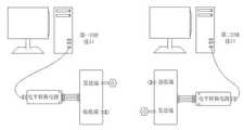
图1是本实用新型所设计的基于USB接口的热插拔可见光无线接入模块的整体框架图。Fig. 1 is an overall frame diagram of a hot-swappable visible light wireless access module based on a USB interface designed in the present invention.
图2是本实用新型所设计的基于USB接口的热插拔可见光无线接入模块中电平转换模块的电路图。Fig. 2 is a circuit diagram of the level conversion module in the hot-swappable visible light wireless access module based on the USB interface designed by the utility model.
图3是本实用新型所设计的基于USB接口的热插拔可见光无线接入模块中发送端电路图。Fig. 3 is a circuit diagram of the transmitter in the hot-swappable visible light wireless access module based on the USB interface designed by the utility model.
图4是本实用新型所设计的基于USB接口的热插拔可见光无线接入模块中接收端电路图。Fig. 4 is a circuit diagram of the receiver in the hot-swappable visible light wireless access module based on the USB interface designed by the utility model.
图5是收发数据指示灯的电路图。Fig. 5 is a circuit diagram of an indicator light for transmitting and receiving data.
图6是本实用新型所设计的基于USB接口的热插拔可见光无线接入模块的整体实物图。Fig. 6 is an overall physical diagram of the hot-swappable visible light wireless access module based on the USB interface designed by the utility model.
图中标号说明:U1为USB接口芯片,U2为 CH430T芯片,U3、U4均为 OPA354芯片,U5为 LT1715芯片,P1为接收端的输出端口,C1至C10为第一至第十电容,R1至R14为第一至第十四电阻,D1、D2为第一、第二二极管,Y1为晶振,L1至L4为第一至第四发光二极管,PD1为光敏二极管。Explanation of the symbols in the figure: U1 is the USB interface chip, U2 is the CH430T chip, U3 and U4 are both OPA354 chips, U5 is the LT1715 chip, P1 is the output port of the receiving end, C1 to C10 are the first to tenth capacitors, R1 to R14 are the first to fourteenth resistors, D1 and D2 are the first and second diodes, Y1 is a crystal oscillator, L1 to L4 are the first to fourth light emitting diodes, and PD1 is a photosensitive diode.
具体实施方式Detailed ways
下面结合附图对本实用新型的技术方案做进一步的详细说明:Below in conjunction with accompanying drawing, the technical scheme of the utility model is described in further detail:
如图1所示的基于USB接口的热插拔可见光无线接入系统,包括第一USB接口、第一电平转换电路、发送端、接收端、第二电平转换电路、第二USB接口。第一USB接口与第一电平转换电路的输入端连接,所述第一电平转换电路的输出端与发送端连接。接收端与第二电平转换电路的输入端连接,所述第二电平转换电路的输出端与第二USB接口连接。发送端包括顺序连接的电压跟随器、LED器件,接收端包括顺序连接的光电检测器、放大器、判决电路。The hot-swappable visible light wireless access system based on a USB interface as shown in FIG. 1 includes a first USB interface, a first level conversion circuit, a sending end, a receiving end, a second level conversion circuit, and a second USB interface. The first USB interface is connected to the input end of the first level conversion circuit, and the output end of the first level conversion circuit is connected to the sending end. The receiving end is connected to the input end of the second level conversion circuit, and the output end of the second level conversion circuit is connected to the second USB interface. The sending end includes sequentially connected voltage followers and LED devices, and the receiving end includes sequentially connected photodetectors, amplifiers, and decision circuits.
第一电平转换电路包括:依次连接的USB接口电路、脉冲编码电路。第二电平转换电路包括:依次连接的脉冲解码电路、USB接口电路。The first level conversion circuit includes: a USB interface circuit and a pulse encoding circuit connected in sequence. The second level conversion circuit includes: a pulse decoding circuit and a USB interface circuit connected in sequence.
第一电平转换电路中:第一USB接口用于接收外部PC等数字设备产生的串行总线信号;接口电路将串行总线信号进行电平转换,由串口电平转化为TTL电平,并传输至脉冲编码电路;脉冲编码电路用于将TTL信号进行脉冲编码调制,并将调制后的信号送入电压跟随器。In the first level conversion circuit: the first USB interface is used to receive the serial bus signal generated by digital equipment such as an external PC; the interface circuit performs level conversion on the serial bus signal, from the serial port level to TTL level, and It is transmitted to the pulse encoding circuit; the pulse encoding circuit is used to perform pulse code modulation on the TTL signal, and send the modulated signal to the voltage follower.
第二电平转换电路中:脉冲解码电路将判决器输出的信号进行脉冲编码解调,恢复出原始传输的TTL电平信号;接口电路将TTL电平信号转换为适合USB传输的串行总线信号。In the second level conversion circuit: the pulse decoding circuit performs pulse code demodulation on the signal output by the decision device to restore the original transmitted TTL level signal; the interface circuit converts the TTL level signal into a serial bus signal suitable for USB transmission .
第一、第二电平转换电路如图2所示,第一电平转换、第二电平转换均通过U2实现。U1为USB接口芯片,U2为电平转换芯片CH430T。U1 USB接口输出的电压经过第一、第二二极管D1、D2后给U2供电,U1的D+引脚、D-引脚接U2的D+引脚、D-引脚,第二电容C2、第三电容C3及晶振电容Y1组成U2的晶振电路,第一电容C1与U2的V3引脚连接后接地,U1的输出电压经过第四电容C4、第五电容C5后与U2电源端连接。The first and second level conversion circuits are shown in FIG. 2 , and both the first level conversion and the second level conversion are realized through U2. U1 is a USB interface chip, and U2 is a level conversion chip CH430T. The voltage output by the USB interface of U1 supplies power to U2 after passing through the first and second diodes D1 and D2. The D+ pin and D- pin of U1 are connected to the D+ pin and D- pin of U2, and the second capacitor C2, The third capacitor C3 and the crystal oscillator capacitor Y1 form the crystal oscillator circuit of U2. The first capacitor C1 is connected to the V3 pin of U2 and then grounded. The output voltage of U1 passes through the fourth capacitor C4 and the fifth capacitor C5 and then connects to the power terminal of U2.
发送端中:电压跟随器采用运算放大器和电阻进行负反馈,在不改变信号电压的情况下,放大信号的电流以驱动LED器件发光,LED器件发光的亮度随驱动电流的强弱而变化。LED器件用于将电信号转换成光信号,并通过无线传输的方式将光信号传输至光电探测器。U3是运放芯片OPA354,U3实现的功能是在不改变信号电压值的情况下放大发送信号的电流值。如图3所示,U3的第2引脚和第6引脚连接,第4引脚接地,第6引脚接第四电阻R4、第四发光二极管L4后接地,第五电阻R5、第六电容C6均并连在第四发光二极管L4的两端。In the sending end: the voltage follower uses operational amplifiers and resistors for negative feedback. Without changing the signal voltage, the current of the signal is amplified to drive the LED device to emit light. The brightness of the LED device's light varies with the strength of the driving current. LED devices are used to convert electrical signals into optical signals, and transmit the optical signals to photodetectors through wireless transmission. U3 is an operational amplifier chip OPA354, and the function realized by U3 is to amplify the current value of the transmitted signal without changing the signal voltage value. As shown in Figure 3, the 2nd pin of U3 is connected to the 6th pin, the 4th pin is grounded, the 6th pin is connected to the fourth resistor R4, the fourth light-emitting diode L4 and then grounded, the fifth resistor R5, the sixth The capacitors C6 are connected in parallel to both ends of the fourth light emitting diode L4.
接收端中,光电探测器用于接收光信号,并将光信号转换为电信号后传输至放大器;放大器用于将电信号进行电压放大和电流放大,使放大后电信号的电平值满足判决要求。在具体的实施例中,放大器为由芯片U4、第九电阻R9、第十电阻R10、第十一电阻R11、第十电容C10构成的前置跨阻放大器,同时前置跨阻放大器完成宽带放大器的功能,前置跨阻放大器具有较高的增益,当输入信号为高频信号时能够有效减少前端噪声,保持较高的灵敏度,降低由于放大产生的错误码元数;宽带放大器在较宽的频率范围内具有均匀的放大增益,用于将前置跨阻放大器输出的信号进行宽带放大。判决器模块由芯片U5、第十二电阻R12、第十三电阻R13、第十四电阻R14构成,用于对接收电信号的电平值进行抽样判决,并将判决后的信号传输至脉冲解码电路。如图4所示,U4是运放芯片OPA354,实现的功能是对PD光电转换后的微弱电流信号进行前置跨阻放大;U5是比较器芯片LT1715,将接收到的信号进行判决,恢复原始发送信号;P1是接收端的输出端口,输出TTL电平。光敏二极管PD1的阳极接第七电容C7后接地,光敏二极管PD1的阴极、第九电容C9的一极分别与第六电阻R6的一端连接;第七电阻R7的一端、第九电容C9的另一极、第七电阻R7的另一端分别与第八电阻R8的一端连接;第八电阻R8的另一端与U4的2号引脚连接,第八电阻R8串联连接第九电阻R9、第十电阻R10、第十电容C10后接地;U4的7号引脚与VCC直流电压源连接;第十一电阻R11的一端接地,另一端接U5的1号引脚;第十二电阻R12跨接在U5的1号、10号引脚之间;R5的9号引脚、10号引脚分别与第八电容C8的正极连接;第十三电阻R13的一端接U5的8号引脚,另一端与第十四电阻R14的一端、P1的4号引脚;第六电阻R6的另一端,第七电阻R7的一端,第八电容C8的负极,第十四电阻R14的另一端,U4的3号引脚、4号引脚,U5的2号、5号引脚,P1的3号引脚接地。In the receiving end, the photodetector is used to receive the optical signal, convert the optical signal into an electrical signal and transmit it to the amplifier; the amplifier is used to amplify the voltage and current of the electrical signal, so that the level value of the amplified electrical signal meets the judgment requirements . In a specific embodiment, the amplifier is a pre-transimpedance amplifier composed of the chip U4, the ninth resistor R9, the tenth resistor R10, the eleventh resistor R11, and the tenth capacitor C10. At the same time, the pre-transimpedance amplifier completes the broadband amplifier The function of the pre-transimpedance amplifier has a high gain. When the input signal is a high-frequency signal, it can effectively reduce the front-end noise, maintain high sensitivity, and reduce the number of error symbols caused by amplification; It has a uniform amplification gain in the frequency range and is used to amplify the signal output by the pre-transimpedance amplifier in a broadband manner. The decider module is composed of chip U5, the twelfth resistor R12, the thirteenth resistor R13, and the fourteenth resistor R14, which are used to sample and judge the level value of the received electrical signal, and transmit the judged signal to the pulse decoding circuit. As shown in Figure 4, U4 is the operational amplifier chip OPA354, which realizes the pre-transimpedance amplification of the weak current signal after PD photoelectric conversion; U5 is the comparator chip LT1715, which judges the received signal and restores the original Send signal; P1 is the output port of the receiving end, which outputs TTL level. The anode of the photodiode PD1 is connected to the seventh capacitor C7 and grounded, and the cathode of the photodiode PD1 and one pole of the ninth capacitor C9 are respectively connected to one end of the sixth resistor R6; one end of the seventh resistor R7 is connected to the other end of the ninth capacitor C9 pole and the other end of the seventh resistor R7 are respectively connected to one end of the eighth resistor R8; the other end of the eighth resistor R8 is connected to the No. 2 pin of U4, and the eighth resistor R8 is connected in series with the ninth resistor R9 and the tenth resistor R10 , The tenth capacitor C10 is grounded; the No. 7 pin of U4 is connected to the VCC DC voltage source; one end of the eleventh resistor R11 is grounded, and the other end is connected to the No. 1 pin of U5; the twelfth resistor R12 is connected across U5 Between No. 1 and No. 10 pins; No. 9 and No. 10 pins of R5 are respectively connected to the positive pole of the eighth capacitor C8; one end of the thirteenth resistor R13 is connected to No. 8 pin of U5, and the other end is connected to No. 8 pin of U5 One end of the fourteenth resistor R14, the No. 4 pin of P1; the other end of the sixth resistor R6, one end of the seventh resistor R7, the negative pole of the eighth capacitor C8, the other end of the fourteenth resistor R14, and the No. 3 pin of
第二USB接口用于接收上述串行总线电平信号,并由PC等数字设备进行下一步的读取等操作。The second USB interface is used to receive the above-mentioned serial bus level signal, and a digital device such as a PC performs further operations such as reading.
作为进一步的优化方案:为了能够使光电探测器达到更好的效果,可在光电探测器的输入端设置滤光和聚光器件,将LED器件发出的光经过滤波后聚焦到光电探测器的感光部分,从而提高光电探测器的灵敏性;As a further optimization scheme: In order to achieve better results for the photodetector, a filter and light concentrating device can be set at the input end of the photodetector, and the light emitted by the LED device can be filtered and then focused to the light-sensitive area of the photodetector. part, thereby improving the sensitivity of the photodetector;
作为进一步的优化方案:LED器件采用白光LED器件,能够在照明的同时高速响应。As a further optimization scheme: the LED device adopts a white light LED device, which can respond at a high speed while illuminating.
如图5所示的收发数据指示电路:第一电阻R1、第一发光二极管L1组成的串联支路,第二电阻R2、第二发光二级管L2组成的串联支路,第三电阻R3、第三发光二级管L3组成的串联支路,并联连接;每一个串联支路由直流电压源供电,发光二级管的阴极接地。发送端工作时,第二发光二级管L2亮;接收端工作时,第三发光二级管L3亮。The sending and receiving data indication circuit shown in Figure 5: a series branch composed of the first resistor R1 and the first light-emitting diode L1, a series branch composed of the second resistor R2 and the second light-emitting diode L2, the third resistor R3, The series branches formed by the third light-emitting diode L3 are connected in parallel; each series branch is powered by a DC voltage source, and the cathode of the light-emitting diode is grounded. When the sending end is working, the second light-emitting diode L2 is on; when the receiving end is working, the third light-emitting diode L3 is on.
如图6所示,在实际应用中,将发送端与接收端均封装在一个壳体内,发送端、接收端通过壳体上的接口与电平转换电路连接后接USB接口。根据需求,当可见光无线接入系统接收PC机发出的信息时,USB接口、电平转换电路、发送端构成可见光无线接入系统的发送端;当可见光无线接入系统接收LED器件发出的信息时,接收端、电平转换电路、USB接口构成可见光无线接入系统的接收端,实现双工通信。As shown in FIG. 6 , in practical applications, both the transmitting end and the receiving end are packaged in a housing, and the transmitting end and the receiving end are connected to the level conversion circuit through the interface on the housing and then connected to the USB interface. According to requirements, when the visible light wireless access system receives the information sent by the PC, the USB interface, the level conversion circuit, and the sending end constitute the sending end of the visible light wireless access system; when the visible light wireless access system receives the information sent by the LED device , the receiving end, the level conversion circuit, and the USB interface constitute the receiving end of the visible light wireless access system to realize duplex communication.
综上所述,本实用新型利用USB接口实现可见光无线接入系统作为终端接入无线局域网或无线个域网,同时通过USB获取工作电压,简化了电路设计;支持高速数字信号的双工传输,实现不受电磁干扰的大容量短距离无线通信。上述实施例只是本实用新型的一个具体实施例,凡是符合本专利实用新型宗旨的实施例均在本实用新型的保护范围之内。In summary, the utility model uses the USB interface to realize the visible light wireless access system as a terminal to access the wireless local area network or wireless personal area network, and at the same time obtains the working voltage through the USB, which simplifies the circuit design; supports duplex transmission of high-speed digital signals, Realize high-capacity short-distance wireless communication free from electromagnetic interference. The above-mentioned embodiment is only a specific embodiment of the utility model, and all embodiments conforming to the purpose of the utility model of the patent are within the scope of protection of the utility model.
Claims (5)
Translated fromChinesePriority Applications (1)
| Application Number | Priority Date | Filing Date | Title |
|---|---|---|---|
| CN 201220466345CN202772896U (en) | 2012-09-14 | 2012-09-14 | USB interface based hot plug visible light wireless access system |
Applications Claiming Priority (1)
| Application Number | Priority Date | Filing Date | Title |
|---|---|---|---|
| CN 201220466345CN202772896U (en) | 2012-09-14 | 2012-09-14 | USB interface based hot plug visible light wireless access system |
Publications (1)
| Publication Number | Publication Date |
|---|---|
| CN202772896Utrue CN202772896U (en) | 2013-03-06 |
Family
ID=47779437
Family Applications (1)
| Application Number | Title | Priority Date | Filing Date |
|---|---|---|---|
| CN 201220466345Expired - Fee RelatedCN202772896U (en) | 2012-09-14 | 2012-09-14 | USB interface based hot plug visible light wireless access system |
Country Status (1)
| Country | Link |
|---|---|
| CN (1) | CN202772896U (en) |
Cited By (2)
| Publication number | Priority date | Publication date | Assignee | Title |
|---|---|---|---|---|
| CN103490814A (en)* | 2013-09-25 | 2014-01-01 | 上海理工大学 | Serial communication device of USB interface LED visible light and system thereof |
| CN103763031A (en)* | 2014-01-27 | 2014-04-30 | 惠州Tcl移动通信有限公司 | Communication terminal and communication system achieving communication through visible light |
- 2012
- 2012-09-14CNCN 201220466345patent/CN202772896U/ennot_activeExpired - Fee Related
Cited By (3)
| Publication number | Priority date | Publication date | Assignee | Title |
|---|---|---|---|---|
| CN103490814A (en)* | 2013-09-25 | 2014-01-01 | 上海理工大学 | Serial communication device of USB interface LED visible light and system thereof |
| CN103763031A (en)* | 2014-01-27 | 2014-04-30 | 惠州Tcl移动通信有限公司 | Communication terminal and communication system achieving communication through visible light |
| US9577754B2 (en) | 2014-01-27 | 2017-02-21 | Huizhou Tcl Mobile Communication Co., Ltd. | Nonradiative communication terminal and communication system using visible light for communication |
Similar Documents
| Publication | Publication Date | Title |
|---|---|---|
| CN102882600A (en) | Universal serial bus (USB)-interface-based pluggable visible like wireless access system | |
| CN103338072B (en) | Based on visible light communication and the radio switch-in method of android system | |
| CN204498130U (en) | Photoelectric switching circuit and optical signal receiver | |
| CN105897335A (en) | USB interface communication handheld transmitting and receiving device based on visible light communication technology | |
| CN203933634U (en) | A kind of device of visible light communication | |
| CN104734785B (en) | A kind of visible optical pickup apparatus and visible method for optical reception | |
| CN103532625A (en) | White-light LED (light-emitting diode) speech signal communication transceiving system | |
| CN103825656A (en) | Visible light communication system based on TCP/IP and method | |
| CN203554545U (en) | Handset internet-surfing device based on visible-light communication | |
| CN205596120U (en) | High -speed LED visible light communication system and receiving arrangement | |
| CN207559999U (en) | A kind of converged communication device of combination visible light communication | |
| CN202750093U (en) | System for recognizing lamp ID information by LED (light-emitting diode) white light | |
| CN202857947U (en) | Mine helmet based on visible light wireless communication module | |
| CN215378927U (en) | Audio transmission system based on visible light communication | |
| CN109756269A (en) | A kind of visible light communication receiving circuit | |
| CN102594460A (en) | Deflection-type LED (light-emitting diode) optical communication transceiver | |
| CN102314765A (en) | Plastic optical fiber network electricity checks meter system | |
| CN202772896U (en) | USB interface based hot plug visible light wireless access system | |
| CN108199771A (en) | A kind of visible light communication device | |
| CN205039821U (en) | Apply to LED visible light communication system of audio signal transmission | |
| CN110739996A (en) | LED-based visible light communication transmission equipment | |
| CN205693676U (en) | An LED-based wireless optical access network device | |
| CN105610512A (en) | DC-20Mbps low-rate double-reception SFP optical module | |
| CN102811092A (en) | Point-to-point visible light wireless communication system based on white LED devices | |
| CN208158589U (en) | A kind of visible light communication device |
Legal Events
| Date | Code | Title | Description |
|---|---|---|---|
| C14 | Grant of patent or utility model | ||
| GR01 | Patent grant | ||
| CF01 | Termination of patent right due to non-payment of annual fee | Granted publication date:20130306 Termination date:20150914 | |
| EXPY | Termination of patent right or utility model |