CN202495007U - touch pad - Google Patents
touch padDownload PDFInfo
- Publication number
- CN202495007U CN202495007UCN 201120438435CN201120438435UCN202495007UCN 202495007 UCN202495007 UCN 202495007UCN 201120438435CN201120438435CN 201120438435CN 201120438435 UCN201120438435 UCN 201120438435UCN 202495007 UCN202495007 UCN 202495007U
- Authority
- CN
- China
- Prior art keywords
- inductive layer
- layer
- sensing layer
- sensing
- touch pad
- Prior art date
- Legal status (The legal status is an assumption and is not a legal conclusion. Google has not performed a legal analysis and makes no representation as to the accuracy of the status listed.)
- Expired - Fee Related
Links
- 239000000758substrateSubstances0.000claimsabstractdescription8
- 239000000463materialSubstances0.000claimsdescription21
- 230000001939inductive effectEffects0.000claimsdescription20
- 229920000728polyesterPolymers0.000claimsdescription10
- 230000003287optical effectEffects0.000claimsdescription5
- 239000011347resinSubstances0.000claimsdescription4
- 229920005989resinPolymers0.000claimsdescription4
- 239000011248coating agentSubstances0.000claimsdescription3
- 238000000576coating methodMethods0.000claimsdescription3
- 230000002093peripheral effectEffects0.000claimsdescription2
- 238000009413insulationMethods0.000claims8
- 230000005540biological transmissionEffects0.000claims4
- 239000004568cementSubstances0.000claims2
- 239000012528membraneSubstances0.000claims2
- 230000015572biosynthetic processEffects0.000claims1
- 239000010410layerSubstances0.000abstractdescription91
- 238000002834transmittanceMethods0.000abstractdescription10
- 239000002344surface layerSubstances0.000abstractdescription8
- 230000006698inductionEffects0.000abstractdescription3
- 238000005452bendingMethods0.000abstract1
- 239000010408filmSubstances0.000description22
- 239000003292glueSubstances0.000description7
- 125000006850spacer groupChemical group0.000description6
- 239000004020conductorSubstances0.000description5
- 230000000694effectsEffects0.000description5
- 230000035945sensitivityEffects0.000description4
- 230000008859changeEffects0.000description3
- AMGQUBHHOARCQH-UHFFFAOYSA-Nindium;oxotinChemical compound[In].[Sn]=OAMGQUBHHOARCQH-UHFFFAOYSA-N0.000description3
- 238000000034methodMethods0.000description3
- 229920003229poly(methyl methacrylate)Polymers0.000description3
- 229920000515polycarbonatePolymers0.000description3
- 239000004417polycarbonateSubstances0.000description3
- 239000004926polymethyl methacrylateSubstances0.000description3
- YVTHLONGBIQYBO-UHFFFAOYSA-Nzinc indium(3+) oxygen(2-)Chemical compound[O--].[Zn++].[In+3]YVTHLONGBIQYBO-UHFFFAOYSA-N0.000description3
- 230000004888barrier functionEffects0.000description2
- 239000011521glassSubstances0.000description2
- 239000002131composite materialSubstances0.000description1
- 229920001577copolymerPolymers0.000description1
- 238000006073displacement reactionMethods0.000description1
- RHZWSUVWRRXEJF-UHFFFAOYSA-Nindium tinChemical compound[In].[Sn]RHZWSUVWRRXEJF-UHFFFAOYSA-N0.000description1
- 238000003475laminationMethods0.000description1
- 239000011159matrix materialSubstances0.000description1
- 229910052751metalInorganic materials0.000description1
- 239000002184metalSubstances0.000description1
- 230000004048modificationEffects0.000description1
- 238000012986modificationMethods0.000description1
- 230000003647oxidationEffects0.000description1
- 238000007254oxidation reactionMethods0.000description1
- 238000004544sputter depositionMethods0.000description1
- 239000010409thin filmSubstances0.000description1
- 230000001960triggered effectEffects0.000description1
Images


Landscapes
- Position Input By Displaying (AREA)
Abstract
Description
Translated fromChinese技术领域technical field
本实用新型涉及一种多任务触摸板,尤指一种同时具备电容式及电阻式触控感应接口的叠层触摸板。 The utility model relates to a multi-task touch panel, in particular to a laminated touch panel with capacitive and resistive touch sensing interfaces. the
背景技术Background technique
触摸板已被广泛应用于各项电子产品上,例如,电阻式触摸板常被配置在个人数字助理(PDA)、电子字典、手机、MP3数字播放器或卫星导航仪(GPS)等小型电子产品的屏幕上使用,而电容式触摸板则大多应用作为笔记本电脑的鼠标板、虚拟触摸按键等。 Touch panels have been widely used in various electronic products. For example, resistive touch panels are often configured in small electronic products such as personal digital assistants (PDAs), electronic dictionaries, mobile phones, MP3 digital players, or satellite navigation systems (GPS). It is used on the screen, while the capacitive touch pad is mostly used as the mouse pad of the notebook computer, virtual touch buttons, etc. the
一般电容式触摸板是由使用者的手指或导体碰触或轻滑过触摸板表面的瞬间产生一个电容效应,利用控制电路即可由电容值的变化确定手指或导体的碰触位置;由于电容式触摸板可用手指进行输入,具有输入操作便利的特点,而其输入操作不需经过触压,不会让面板有承受反复应力、变形导致损害的缺点;使用手指输入虽然非常方便,但是手指输入方式感应的准确度不高,容易产生误操作,造成使用上的的困扰。电阻式触摸板可使用笔尖进行精准的触压位置操作,因此可应用在较小的使用面积或较高精度的点位输入,尤其适合用于笔划较多或形体复杂的文字辨识的输入操作;但电阻式触摸板由触压面板的输入操作方式,会使板体内部的导电膜承受反复应力、应变导致损害,故使用寿命有限。 Generally, a capacitive touch panel produces a capacitive effect when the user's finger or conductor touches or slides lightly across the surface of the touch panel, and the touch position of the finger or conductor can be determined by the change of the capacitance value by using the control circuit; The touchpad can be used for input with fingers, which has the characteristics of convenient input operation, and its input operation does not need to go through touch pressure, which will not cause the panel to suffer repeated stress and deformation to cause damage; although it is very convenient to use finger input, the finger input method The accuracy of the induction is not high, and it is easy to cause misoperation, causing troubles in use. The resistive touchpad can use the tip of the pen to perform precise touch position operation, so it can be applied to a small use area or a high-precision point input, especially suitable for the input operation of character recognition with many strokes or complex shapes; However, the input operation mode of the touch panel of the resistive touch panel will cause the conductive film inside the panel to withstand repeated stress and strain to cause damage, so the service life is limited. the
如前述说明,常用电容式触摸板及电阻式触摸板均各具功能特色与优缺 点,因此,整合前述二种触摸板的功能与优点一直是业界努力的目标,而目前已知的手段是将现有的电容式触摸板结构与电阻式触摸板结构,二者上下叠合成一板体,这种复合触摸板虽可形成在一板体上同时具备电容式与电阻式二种触控感应效能,但因其组合结构的叠层较多,导致位于下方的电阻式触摸板的触控感应效果的敏感性与精确度降低,且因板体变得较厚重,将严重减损其光学特性,造成模糊或失真的困扰。 As mentioned above, the commonly used capacitive touch panels and resistive touch panels have their own functional characteristics and advantages and disadvantages. Therefore, integrating the functions and advantages of the aforementioned two touch panels has always been the goal of the industry, and the currently known means are The existing capacitive touch panel structure and resistive touch panel structure are stacked up and down to form a board body. Although this composite touch panel can be formed on a board body, it has both capacitive and resistive touch sensors. performance, but because of the many stacked layers of the combined structure, the sensitivity and accuracy of the touch sensing effect of the resistive touch panel located below will be reduced, and because the board becomes thicker, its optical characteristics will be seriously degraded. Trouble with blurring or distortion. the
发明内容Contents of the invention
鉴于现有技术的上述缺点,本实用新型提供一种改良的触摸板,其将电容式触摸板及电阻式触摸板整合成一板体,兼具二种触摸板的效能与优点,并减化部分叠层设置,以提升位于下方的电阻式触摸板的触控感应效果的敏感性与精确度,同时降低板体厚度,以增进整体触摸板的透明度,方便观看。 In view of the above-mentioned shortcomings of the prior art, the utility model provides an improved touch panel, which integrates the capacitive touch panel and the resistive touch panel into one panel body, has both the performance and advantages of the two types of touch panels, and reduces part Lamination is arranged to improve the sensitivity and accuracy of the touch sensing effect of the resistive touch panel located below, while reducing the thickness of the panel body to enhance the transparency of the overall touch panel for easy viewing. the
为了达成上述目的,本实用新型所提供的触摸板,其包含一可弯曲高透光率的表面层;第一感应层,为一透明导电薄膜,其含有多道彼此平行排列的第一轴向线迹,各个第一轴向线迹是由多个电容感应单元彼此相连接组成,且各个第一轴向线迹的一端缘分别电接于设在面板边缘的信号线路;一可弯曲高透光率的绝缘层;第二感应层,为具有良好导电特性的透明薄膜,其含有多道彼此平行排列的第二轴向线迹,各个第二轴向线迹是由多个电容感应单元彼此相连接组成,且各个第二轴向线迹的一端缘分别电接于设在面板边缘的信号线路;第三感应层,为设有电子节点且具有良好导电特性的透明导电膜,并在导电膜表面设置多个间隔球,并使四周缘分别电接于设在面板边缘的信号线路;以及一透光性的基板;上述各层被依序叠接组合成一透明板 体,使第一轴向线迹与第二轴向线迹彼此呈约90°设置,而第二感应层与第三感应层之间由所述间隔球,以将彼此分开成一定间隙而对向配置,因此前述第一感应层与第二感应层可共同构成一电容式触控感应回路,而第二感应层与第三感应层共同构成一电阻式触控感应回路。 In order to achieve the above object, the touch panel provided by the utility model includes a flexible surface layer with high light transmittance; the first sensing layer is a transparent conductive film, which contains a plurality of parallel first axial layers Each first axial trace is composed of a plurality of capacitive sensing units connected to each other, and one end edge of each first axial trace is respectively electrically connected to the signal line provided on the edge of the panel; a bendable high-transparency The insulating layer of light rate; the second sensing layer is a transparent film with good conductive properties, which contains multiple second axial traces arranged in parallel with each other, and each second axial trace is formed by a plurality of capacitive sensing units. connected to each other, and one edge of each second axial trace is electrically connected to the signal line on the edge of the panel; the third sensing layer is a transparent conductive film with electronic nodes and good conductive properties, and is conductive A plurality of spacer balls are arranged on the surface of the film, and the surrounding edges are respectively electrically connected to the signal lines provided on the edge of the panel; and a light-transmitting substrate; the above-mentioned layers are sequentially stacked and combined to form a transparent plate, so that the first axis The direction stitches and the second axial stitches are arranged at about 90° to each other, and the spacer balls are arranged between the second sensing layer and the third sensing layer to separate each other into a certain gap, so the aforementioned first The first sensing layer and the second sensing layer can jointly form a capacitive touch sensing loop, and the second sensing layer and the third sensing layer can jointly form a resistive touch sensing loop. the
特别是,该表面层为一具有可弯曲、高透光率的绝缘薄膜,其材料是选自于聚酯(PET)或聚碳酸酯(PC)等,但实施的材料范围不以前述材料为限;而该绝缘层也可为一具有可弯曲、高透光率的绝缘薄膜,其材料是选自于聚酯、油墨、光硬化树脂(UV胶)或光学胶(OCA胶)等,但实施的材料范围不以前述材料为限;第一感应层与第二感应层是使用具有良好导电特性的氧化铟锡(ITO)或氧化铟锌等材质的透明薄膜,而且利用蚀刻制程在该透明薄膜上形成多个彼此等距平行排列的透明线迹。该基板为一坚硬材质的透明薄板,其材料是选自于玻璃或聚碳酸酯(PC)、聚酯(PET)、聚甲基丙烯酸甲酯(PMMA)或环烯烃共聚合物(COC)等,但实施的材料范围不以前述材料为限。 In particular, the surface layer is an insulating film with flexibility and high light transmittance, and its material is selected from polyester (PET) or polycarbonate (PC), etc., but the range of materials implemented is not limited to the aforementioned materials. and the insulating layer can also be a flexible, high-transmittance insulating film whose material is selected from polyester, ink, light-curing resin (UV glue) or optical glue (OCA glue), etc., but The range of implemented materials is not limited to the aforementioned materials; the first sensing layer and the second sensing layer are made of transparent films such as indium tin oxide (ITO) or indium zinc oxide with good electrical conductivity, and are etched on the transparent A plurality of transparent traces arranged equidistantly and parallel to each other are formed on the film. The substrate is a hard transparent thin plate, and its material is selected from glass or polycarbonate (PC), polyester (PET), polymethyl methacrylate (PMMA) or cycloolefin copolymer (COC), etc. , but the range of implemented materials is not limited to the aforementioned materials. the
在一实施例中,本实用新型的触摸板还包含在第二感应层与第三感应层之间设置有:一可弯曲高透光率的第二绝缘层;以及第四感应层,为设有电子节点的透明导电膜,在该导电膜的四周缘分别电接于设在面板边缘的信号线路;使第四感应层与第三感应层之间由所述间隔球,以将彼此分开成一定间隙而对向配置,因此由第四感应层与第三感应层共同构成一电阻式触控感应回路。 In one embodiment, the touch panel of the present invention further includes: a flexible second insulating layer with high light transmittance; and a fourth sensing layer, which is provided between the second sensing layer and the third sensing layer A transparent conductive film with electronic nodes is electrically connected to the signal lines on the edge of the panel at the periphery of the conductive film; the fourth sensing layer and the third sensing layer are separated by the spacer balls to separate each other into They are disposed opposite to each other with a certain gap, so the fourth sensing layer and the third sensing layer together form a resistive touch sensing circuit. the
特别是,第二绝缘层为一具有可弯曲、高透光率的绝缘薄膜,其材料是选自于聚酯、油墨、光硬化树脂(UV胶)或光学胶(OCA胶)等,但实施的材料范围不以前述材料为限;而第三感应层与第四感应层是使用具有良好导电特 性的氧化铟锡或氧化铟锌等材质的透明薄膜。 In particular, the second insulating layer is a flexible, high-transmittance insulating film, and its material is selected from polyester, ink, light-hardening resin (UV glue) or optical glue (OCA glue), etc., but the implementation The range of materials is not limited to the aforementioned materials; and the third sensing layer and the fourth sensing layer are transparent films made of materials such as indium tin oxide or indium zinc oxide with good electrical conductivity. the
本实用新型的触摸板,兼具容式触摸板及电阻式触摸板二种触摸板的效能与优点,同时降低板体厚度,以增进整体触摸板的透明度,方便观看。 The touch panel of the utility model has the performance and advantages of both the capacitive touch panel and the resistive touch panel, and at the same time reduces the thickness of the panel body to increase the transparency of the overall touch panel and facilitate viewing. the
附图说明Description of drawings
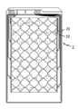
图1为本实用新型的侧面部分剖示图; Fig. 1 is the side part sectional view of the utility model;
图2为本实用新型另一实施例的侧面部分剖示图; Fig. 2 is the side part sectional view of another embodiment of the utility model;
图3为本实用新型的X轴感应层的电容感应单元排列图形; Fig. 3 is the arrangement figure of the capacitive sensing unit of the X-axis sensing layer of the present invention;
图4为本实用新型的Y轴感应层的电容感应单元排列图形; Fig. 4 is the arrangement pattern of the capacitive sensing unit of the Y-axis sensing layer of the present invention;
图5为本实用新型的构件组合的平面图; Fig. 5 is the plan view of component combination of the present utility model;
图6为本实用新型的另一种X轴感应层的电容感应单元排列图形; Fig. 6 is another kind of capacitive sensing element arrangement pattern of X-axis sensing layer of the present utility model;
图7为本实用新型的另一种Y轴感应层的电容感应单元排列图形;以及 Fig. 7 is another kind of capacitive sensing unit arrangement pattern of Y-axis sensing layer of the present utility model; And
图8为本实用新型另一种实施例的构件组合的平面图。 Fig. 8 is a plan view of component assembly of another embodiment of the present invention. the
具体实施方式Detailed ways
如图1所示是本实用新型的优选实施例,其主要包含一表面层1、一X轴感应层2、一绝缘层3、一Y轴感应层4、一电阻感应层5以及一基板6,上述各层被依序叠接组合成一多任务触摸板;在这个实施例中,该表面层1是选用聚酯材料制成的可弯曲、高透光率的绝缘薄膜,而绝缘层3则是由油墨材料涂布形成的可弯曲、高透光率的绝缘薄层;前述X轴感应层2、Y轴感应层4与电阻感应层5使用具有良好导电特性的透明导电膜,例如氧化铟锡或氧化铟锌薄膜;其中,在X轴感应层2的透明导电膜上具有数道彼此平行排列的X轴感应线迹,各个X轴感应线迹具有多个彼此相连接的电容感应单元22,而该电容感应单元22的图形可为向X轴方向延伸的菱形面积(如图3 所示)或矩形面积(如图6所示),且令前述各X轴线迹的一端缘分别电接于设在面板边缘的信号线路23;同样的,在Y轴感应层4的透明导电膜上具有数道彼此平行排列的Y轴感应线迹,各个Y轴感应线迹具有多个彼此相连接的电容感应单元42,而该电容感应单元的图形可为向Y轴方向延伸的菱形面积(如图4所示)或矩形面积(如图7所示),且令前述各Y轴线迹的一端缘分别电接于设在面板边缘的信号线路43;而该电阻感应层5是一设有电子节点的透明导电膜,且在导电膜表面设有多个均匀分布的间隔球51,令前述电阻感应层5的四周缘分别电接于设在面板边缘的信号线路53;该基板6是使用具坚硬材质的透明板料,例如透明玻璃、聚碳酸酯或聚甲基丙烯酸甲酯等薄板;另外,在该表面层1的底表面靠近外周缘部位还设有金属溅镀形成的有颜色框罩12,其恰可用以遮蔽上述设在面板边缘的信号线路23、43、53,以达美观效果。 As shown in Figure 1 is a preferred embodiment of the present utility model, which mainly includes a
再请参阅图5、8所示,将前述各层被依序叠接组合成一多任务触摸板,其中,X轴感应层2设置在表面层1的底表面,Y轴感应层4隔着绝缘层3与X轴感应层2叠置黏合成一体,并使Y轴感应线迹与X轴线迹之间呈正交设置,Y、X轴感应线迹上的各个电容感应单元42、22略呈矩阵状排列设置;而电阻感应层5设置在基板6的上表面,并利用设在面板周缘部位的绝缘胶54与Y轴感应层4的底面黏合成一体,且在Y轴感应层4与电阻感应层5之间由该间隔球51,以将彼此分开成一定间隙而对向配置。 Referring again to Fig. 5 and shown in Fig. 8, the aforementioned layers are sequentially stacked and combined into a multi-tasking touch panel, wherein the
如前所述的触摸板,在X轴感应层2与Y轴感应层4形成一电容式触控感应回路,因此当手指或导体碰触或轻滑过表面层1时,即可触发电容信号通过信号线路23、43传送到后续的信号处理电路,信号处理电路由电容的变 化,即可判断导体或手指的碰触位置;另外,在Y轴感应层4与电阻感应层5形成一电阻式触控感应回路,当以笔尖触压触摸板时,使触压点部位的Y轴感应层4的向下位移与电阻感应层5电接导通以触发感应信号,而感应信号通过信号线路43、53传送到后续的信号处理电路,信号处理电路藉由感应信号的变化,即可判断笔尖的碰触位置;由于设置在前述电阻式触控感应回路上方的叠层均为可弯曲薄层且厚度非常薄,所以在笔尖触压操作时不会减损该电阻式触控感应回路之触压感应的敏感度,但却可缓和Y轴感应层4与电阻感应层5的氧化铟锡薄膜材料所受的应力冲击,避免锐缘应变的破坏,以延长使用寿命。 As mentioned above, a capacitive touch sensing circuit is formed on the
本实用新型的多任务触摸板为一具有高透明度的板体,可配置在电子产品的显示屏前,让用户可通过屏幕画面上的指示以手指、导体或笔尖等轻触于面板所需位置,即可便利进行输入操作;可以理解的,该触摸板运作时可由信号处理电路的设计,以自动判别或手工切换的方式,选择有效的触控感应信号是来自前述电容式及电阻式触控感应回路或其中之一。 The multi-tasking touch panel of the utility model is a panel with high transparency, which can be arranged in front of the display screen of an electronic product, so that the user can lightly touch the required position of the panel with a finger, a conductor or a pen tip through the instructions on the screen , which can facilitate the input operation; it can be understood that when the touch panel is in operation, the design of the signal processing circuit can automatically distinguish or manually switch, and the effective touch sensing signal is selected from the aforementioned capacitive and resistive touch. induction loop or one of them. the
综上说明可知,本实用新型将电容式触摸板及电阻式触摸板整合成一板体,兼具二种触摸板的效能与优点,并减化部分叠层设置,以提升位于下方的电阻式触摸板的触控感应效果的敏感性与精确度,同时降低板体厚度,以增进整体触摸板的透明度,方便观看。 To sum up, it can be seen that the utility model integrates the capacitive touch panel and the resistive touch panel into one panel body, which has both the performance and advantages of the two touch panels, and reduces part of the stacking arrangement to improve the resistive touch panel located below. The sensitivity and accuracy of the touch sensing effect of the panel are improved, and the thickness of the panel body is reduced at the same time, so as to enhance the transparency of the overall touch panel and facilitate viewing. the
再如图2所示是本实用新型的另一实施例,其整体结构略是与前述实施例相同,主要差异是在Y轴感应层4与电阻感应层5之间增设一绝缘阻隔层8及一上方电阻感应层9;该绝缘阻隔层8为一可弯曲、高透光率的绝缘薄层,例如聚酯薄板或油墨薄膜;该上方电阻感应层9是一设有电子节点的透明导 电膜,且在四周缘分别电接于设在面板边缘的信号线路93;该上方电阻感应层9设置在绝缘阻隔层8的底表面,并利用设在面板周缘部位的绝缘胶54与位在下方的电阻感应层5黏合成一体,且在上方电阻感应层9与电阻感应层5之间由该间隔球51,以将彼此分开成一定间隙而对向配置。依前述构件组成的多任务触摸板,其X轴感应层2与Y轴感应层4共同构成一电容式触控感应回路,而上方电阻感应层9与电阻感应层5共同构成一电阻式触控感应回路,因此可在同一板体上同时兼具有电容式与电阻式触控感应效能。而由上述变更设置也能达成与上一实施例同样的或类似的效能,故其它相同部份在此不再赘述。 As shown in Fig. 2 again, it is another embodiment of the present utility model, and its overall structure is slightly the same as the foregoing embodiment, and the main difference is that an insulating barrier layer 8 is added between the Y-
上述所列举的实施例,仅用为方便说明本实用新型并非加以限制,在不悖离本实用新型精神范畴,熟悉此一行业技艺人士依本实用新型申请专利范围及发明说明所作的各种简易变形与修饰,均仍应含括于以下申请专利范围中。 The above-mentioned embodiments are only used for convenience to illustrate that the utility model is not limited, and without departing from the spirit category of the utility model, familiar with the various simple and simple procedures done by the technical personnel in this industry according to the patent scope of the utility model application and the description of the invention. Deformation and modification should still be included in the scope of the following patent applications. the
Claims (7)
Priority Applications (1)
| Application Number | Priority Date | Filing Date | Title |
|---|---|---|---|
| CN 201120438435CN202495007U (en) | 2011-11-08 | 2011-11-08 | touch pad |
Applications Claiming Priority (1)
| Application Number | Priority Date | Filing Date | Title |
|---|---|---|---|
| CN 201120438435CN202495007U (en) | 2011-11-08 | 2011-11-08 | touch pad |
Publications (1)
| Publication Number | Publication Date |
|---|---|
| CN202495007Utrue CN202495007U (en) | 2012-10-17 |
Family
ID=47001225
Family Applications (1)
| Application Number | Title | Priority Date | Filing Date |
|---|---|---|---|
| CN 201120438435Expired - Fee RelatedCN202495007U (en) | 2011-11-08 | 2011-11-08 | touch pad |
Country Status (1)
| Country | Link |
|---|---|
| CN (1) | CN202495007U (en) |
Cited By (6)
| Publication number | Priority date | Publication date | Assignee | Title |
|---|---|---|---|---|
| CN103019487A (en)* | 2012-11-30 | 2013-04-03 | 深圳市深越光电技术有限公司 | A push-type capacitive screen |
| CN107250943A (en)* | 2015-02-26 | 2017-10-13 | 戴尔产品有限公司 | Touch pad with multiple soft-touch controls |
| CN107678585A (en)* | 2017-09-19 | 2018-02-09 | 深圳市骏达光电股份有限公司 | Touch-screen, touch sensitive layer and preparation method thereof |
| WO2018076997A1 (en)* | 2016-10-27 | 2018-05-03 | 广州视源电子科技股份有限公司 | Touch control panel and touch control module comprising the touch control panel |
| CN108124320A (en)* | 2018-03-02 | 2018-06-05 | 射阳豪越丽玉制品有限公司 | A kind of all fronts temperature control line |
| CN113687732A (en)* | 2020-05-18 | 2021-11-23 | 威斯特克集团公司 | Protected touch sensor and associated touch screen |
- 2011
- 2011-11-08CNCN 201120438435patent/CN202495007U/ennot_activeExpired - Fee Related
Cited By (8)
| Publication number | Priority date | Publication date | Assignee | Title |
|---|---|---|---|---|
| CN103019487A (en)* | 2012-11-30 | 2013-04-03 | 深圳市深越光电技术有限公司 | A push-type capacitive screen |
| CN103019487B (en)* | 2012-11-30 | 2016-01-20 | 深圳市深越光电技术有限公司 | Push type capacitive screen |
| CN107250943A (en)* | 2015-02-26 | 2017-10-13 | 戴尔产品有限公司 | Touch pad with multiple soft-touch controls |
| CN107250943B (en)* | 2015-02-26 | 2021-02-26 | 戴尔产品有限公司 | Touchpad with multiple touch switches |
| WO2018076997A1 (en)* | 2016-10-27 | 2018-05-03 | 广州视源电子科技股份有限公司 | Touch control panel and touch control module comprising the touch control panel |
| CN107678585A (en)* | 2017-09-19 | 2018-02-09 | 深圳市骏达光电股份有限公司 | Touch-screen, touch sensitive layer and preparation method thereof |
| CN108124320A (en)* | 2018-03-02 | 2018-06-05 | 射阳豪越丽玉制品有限公司 | A kind of all fronts temperature control line |
| CN113687732A (en)* | 2020-05-18 | 2021-11-23 | 威斯特克集团公司 | Protected touch sensor and associated touch screen |
Similar Documents
| Publication | Publication Date | Title |
|---|---|---|
| TWI465964B (en) | Touch keyboard and manufacturing method thereof | |
| TWI581161B (en) | Capacitive touch module and touch display apparatus thereof | |
| JP3173195U (en) | Multi-touch pad stack structure | |
| US20100078231A1 (en) | Dual-side integrated touch panel structure | |
| CN103907081A (en) | Touch panel | |
| TWI361997B (en) | ||
| CN202495007U (en) | touch pad | |
| JP2008225980A (en) | Composite touch sensor | |
| CN101727223A (en) | Double-sided composite touch panel structure | |
| CN101320309A (en) | Single-layer touch sensing structure and touch display panel using same | |
| US20210109615A1 (en) | Resistive pressure sensor device system | |
| KR101765950B1 (en) | Touch panel | |
| US20130127777A1 (en) | Multi-processing touch panel assembly | |
| CN106547389A (en) | Display device with pressure sensing function and electronic device | |
| US20120249469A1 (en) | Display with touch control function | |
| CN101470554A (en) | Duplex touch control panel | |
| US20160026284A1 (en) | Circuit connection structure of touch sensor panel | |
| KR101659476B1 (en) | 3D touch screen panel | |
| CN207557916U (en) | A kind of touch screen blast resistance construction | |
| KR20150027384A (en) | Touch panel have digitizer function | |
| CN201152969Y (en) | Improvement of capacitor type touch controlled induction apparatus | |
| GB2456312A (en) | Transparent Capacitive Touch Panel | |
| KR20160018894A (en) | Touch screen panel having pressure sensor | |
| CN204695269U (en) | Built-in type touch display screen and touch display screen module | |
| KR101926587B1 (en) | Touch panel |
Legal Events
| Date | Code | Title | Description |
|---|---|---|---|
| C14 | Grant of patent or utility model | ||
| GR01 | Patent grant | ||
| CF01 | Termination of patent right due to non-payment of annual fee | Granted publication date:20121017 Termination date:20141108 | |
| EXPY | Termination of patent right or utility model |