CN202424561U - Synchronous rectification driving circuit - Google Patents
Synchronous rectification driving circuitDownload PDFInfo
- Publication number
- CN202424561U CN202424561UCN2011204930656UCN201120493065UCN202424561UCN 202424561 UCN202424561 UCN 202424561UCN 2011204930656 UCN2011204930656 UCN 2011204930656UCN 201120493065 UCN201120493065 UCN 201120493065UCN 202424561 UCN202424561 UCN 202424561U
- Authority
- CN
- China
- Prior art keywords
- resistance
- synchronous
- circuit
- voltage
- driving
- Prior art date
- Legal status (The legal status is an assumption and is not a legal conclusion. Google has not performed a legal analysis and makes no representation as to the accuracy of the status listed.)
- Expired - Fee Related
Links
- 230000001360synchronised effectEffects0.000titleclaimsabstractdescription87
- 239000003990capacitorSubstances0.000claimsabstractdescription34
- 238000004804windingMethods0.000claimsabstractdescription25
- 239000004065semiconductorSubstances0.000claims5
- 239000003381stabilizerSubstances0.000claims4
- 239000008186active pharmaceutical agentSubstances0.000claims1
- 238000001514detection methodMethods0.000abstractdescription8
- 238000010586diagramMethods0.000description4
- 238000000034methodMethods0.000description2
- 230000000630rising effectEffects0.000description2
- 238000005070samplingMethods0.000description2
- 230000003139buffering effectEffects0.000description1
- 238000004891communicationMethods0.000description1
- 230000000295complement effectEffects0.000description1
- 230000008878couplingEffects0.000description1
- 238000010168coupling processMethods0.000description1
- 238000005859coupling reactionMethods0.000description1
- 238000013016dampingMethods0.000description1
- 230000007547defectEffects0.000description1
- 230000000694effectsEffects0.000description1
- 238000005516engineering processMethods0.000description1
Images


Classifications
- Y—GENERAL TAGGING OF NEW TECHNOLOGICAL DEVELOPMENTS; GENERAL TAGGING OF CROSS-SECTIONAL TECHNOLOGIES SPANNING OVER SEVERAL SECTIONS OF THE IPC; TECHNICAL SUBJECTS COVERED BY FORMER USPC CROSS-REFERENCE ART COLLECTIONS [XRACs] AND DIGESTS
- Y02—TECHNOLOGIES OR APPLICATIONS FOR MITIGATION OR ADAPTATION AGAINST CLIMATE CHANGE
- Y02B—CLIMATE CHANGE MITIGATION TECHNOLOGIES RELATED TO BUILDINGS, e.g. HOUSING, HOUSE APPLIANCES OR RELATED END-USER APPLICATIONS
- Y02B70/00—Technologies for an efficient end-user side electric power management and consumption
- Y02B70/10—Technologies improving the efficiency by using switched-mode power supplies [SMPS], i.e. efficient power electronics conversion e.g. power factor correction or reduction of losses in power supplies or efficient standby modes
Landscapes
- Rectifiers (AREA)
Abstract
Translated fromChinese
Description
Translated fromChinese技术领域technical field
本实用新型涉及同步整流驱动电路的技术领域,具体地讲,是指一种宽范围输入的同步整流驱动电路。The utility model relates to the technical field of a synchronous rectification drive circuit, in particular to a wide-range input synchronous rectification drive circuit.
背景技术Background technique
同步整流技术目前在业界已日渐成熟,与传统的肖特基二极管整流对比,优势显而易见,随着通讯电子行业的发展,对开关变换器兼容性的要求越来越高,对开关变换器输入电压范围的要求也越来越宽。与此同时,同步整流的驱动电路方式也多样化,而驱动电路的性能对整个开关电源的可靠性影响较大,目前常用的同步整流驱动方式有自驱、他驱或两者相结合,由于自驱结构简单且成本较低,因而得到最为广泛的应用。Synchronous rectification technology is becoming more and more mature in the industry. Compared with the traditional Schottky diode rectification, the advantages are obvious. With the development of the communication electronics industry, the requirements for the compatibility of switching converters are getting higher and higher. The input voltage of switching converters The range of requirements is also getting wider. At the same time, the synchronous rectification drive circuit mode is also diversified, and the performance of the drive circuit has a great influence on the reliability of the entire switching power supply. Currently, the commonly used synchronous rectification drive modes include self-drive, external drive or a combination of the two. The self-propelled structure is simple and the cost is low, so it is the most widely used.
如图1、2所示的自驱结构,驱动电压直接取自主绕组上或通过耦合磁路绕组自驱动。因直接从主绕组上获得驱动电压受主绕组的影响,所以,在实际应用中,使用最多的是通过耦合磁路绕组的自驱动。但这两种自驱动,同步整流管和同步续流管驱动电压的幅值都会受到输入电压变化范围的限制,传统的自驱动只能适应2∶1的输入电压范围,当输入电压范围较宽时,如4∶1的输入电压,由于当输入电压处于高端与低端电压时的占空比的范围变化较大,所以,驱动电压幅值的变化也较大,在实际应用中,会出现驱动电压不足或导致驱动损耗增加,不但影响效率,甚至会损坏器件,不利于其它参数的最优设计。In the self-driving structure shown in Figure 1 and 2, the driving voltage is directly taken from the main winding or self-driven through the coupling magnetic circuit winding. Because the driving voltage obtained directly from the main winding is affected by the main winding, in practical applications, the self-driving through the coupled magnetic circuit winding is the most used. But these two kinds of self-driving, synchronous rectifier tube and synchronous freewheeling tube drive voltage amplitude will be limited by the range of input voltage, the traditional self-drive can only adapt to the input voltage range of 2:1, when the input voltage range is wide When the input voltage is 4:1, because the range of the duty ratio changes greatly when the input voltage is at the high-end and low-end voltages, the amplitude of the driving voltage also varies greatly. In practical applications, there will be Insufficient driving voltage may lead to increased driving loss, which will not only affect the efficiency, but even damage the device, which is not conducive to the optimal design of other parameters.
因此,由于自驱动方式中同步整流管和同步续流管驱动电压的幅值受到输入电压变化范围的限制,严重影响现有自驱动方式在宽范围输入电压的开关变换器中,同步整流电路的通用性和广泛应用性。Therefore, since the amplitude of the driving voltage of the synchronous rectifier tube and the synchronous freewheeling tube in the self-driving mode is limited by the range of the input voltage, it seriously affects the switching converter of the existing self-driving mode in a wide range of input voltage, and the synchronous rectification circuit. Versatility and wide applicability.
实用新型内容Utility model content
本实用新型的目的在于提供一种同步整流驱动电路,其可克服上述缺陷,能适合宽范围输入,且能克服现有电路中同步整流管和同步结流管驱动电压的幅值受到输入电压变化范围限制的不足。The purpose of this utility model is to provide a synchronous rectification drive circuit, which can overcome the above defects, can be suitable for a wide range of input, and can overcome the amplitude of the drive voltage of the synchronous rectifier tube and synchronous junction tube in the existing circuit. Insufficient scope limitation.
为实现上述目的,本实用新型采用如下结构:To achieve the above object, the utility model adopts the following structure:
一种同步整流驱动电路,其用于对同步整流电路进行驱动,与主变压器副边主绕组相连,所述的驱动电路包括运放控制电路、驱动单元及信号检测电路,所述的信号检测电路设于所述的驱动单元与所述的运放控制电路之间;所述的驱动单元包括驱动电容及MOS管。A synchronous rectification drive circuit, which is used to drive the synchronous rectification circuit, and is connected with the main winding of the secondary side of the main transformer. The drive circuit includes an operational amplifier control circuit, a drive unit and a signal detection circuit. The signal detection circuit It is arranged between the driving unit and the operational amplifier control circuit; the driving unit includes a driving capacitor and a MOS transistor.
优选地,上述的驱动电容及MOS管为两组,分别用做同步整流管和同步续流管的驱动。Preferably, the above-mentioned driving capacitors and MOS transistors are in two groups, which are respectively used for driving the synchronous rectifier and the synchronous freewheeling transistor.
优选地,上述的每组驱动电容的两端分别并联于每组MOS管的DS之间,第一组MOS管的D极连接到主变压器副边主绕组的同名端,S极则通过一个电阻连接到同步整流管的G极;第二组中MOS管的D极连接到主变压器副边主绕组的异名端,S极则通过一个电阻连接到同步续流管的G极。Preferably, the two ends of each group of driving capacitors mentioned above are respectively connected in parallel between the DSs of each group of MOS transistors, the D pole of the first group of MOS transistors is connected to the same-named end of the main winding on the secondary side of the main transformer, and the S pole passes through a resistor Connect to the G pole of the synchronous rectifier tube; the D pole of the MOS tube in the second group is connected to the opposite end of the main winding on the secondary side of the main transformer, and the S pole is connected to the G pole of the synchronous freewheeling tube through a resistor.
优选地,上述的运放控制电路包括六个电阻、两个电容及两个比较器,所述电阻一的两端跨接在所述的比较器一的同相输入和输出端,所述电阻二的一端与所述的比较器一的输出相连,所述的电阻二的另一端与第一个MOS的G极相连,所述电阻三的两端跨接在所述的比较器二的同相输入和输出端,所述电阻四的一端与所述的比较器二的输出端相连,另一端与所述的第二个MOS的G极相连,所述电容一的一端与第一个MOS的G极相连,另一端连接到地,电容二的一端与第二个MOS的G极相连,另一端连接到地;电阻五的一端与开关变换器的输出端相连,另一端与电阻六及比较器一的输入端相连,电阻六的另一端接地。Preferably, the above-mentioned operational amplifier control circuit includes six resistors, two capacitors and two comparators, the two ends of the resistor one are connected across the non-inverting input and output terminals of the comparator one, and the resistor two One end of the resistor is connected to the output of the comparator one, the other end of the resistor two is connected to the G pole of the first MOS, and the two ends of the resistor three are connected across the non-inverting input of the comparator two and the output end, one end of the resistor four is connected to the output end of the comparator two, the other end is connected to the G pole of the second MOS, one end of the capacitor one is connected to the G pole of the first MOS One end of capacitor two is connected to the G pole of the second MOS, and the other end is connected to the ground; one end of resistor five is connected to the output end of the switching converter, and the other end is connected to resistor six and the comparator The input terminal of
优选地,上述的信号检测电路包括一个二极管,四个电阻、一个电容和一个稳压管,所述二极管的阳极连接到主变压器副边主绕组的同名端,阴极与电阻一的一端相连,所述的电阻一的另一端与电容一的一端和电阻二的一端相连;所述的电容一的另一端连接到地;所述的电阻二的另一端连接到稳压管的阴极和所述的运放控制电路,所述的稳压管的阳极连接到地,所述的电阻三的一端连接到稳压管的阴极,另一端连接到电阻四的一端和所述的运放控制电路;所述的电阻四的另一端连接到地。Preferably, the above-mentioned signal detection circuit includes a diode, four resistors, a capacitor and a voltage regulator tube, the anode of the diode is connected to the same-named end of the main winding on the secondary side of the main transformer, and the cathode is connected to one end of the resistor one, so The other end of the resistor one is connected to one end of the capacitor one and one end of the resistor two; the other end of the capacitor one is connected to the ground; the other end of the resistor two is connected to the cathode of the voltage regulator tube and the An operational amplifier control circuit, the anode of the voltage regulator tube is connected to the ground, one end of the resistor three is connected to the cathode of the voltage regulator tube, and the other end is connected to one end of the resistor four and the operational amplifier control circuit; The other end of the resistor four mentioned above is connected to the ground.
采用上述技术方案后,使用时,通过控制MOS管的导通与关断,实现了驱动电容与MOS管的分段驱动,输入电压范围可以扩大到4∶1,甚至更宽,更重要的是使同步整流管和同步续流管驱动电压的幅值在整个输入电压范围内得到合理分配,避免了同步整流管或同步续流管的损坏,降低了驱动电路带来的损耗,提高了整机的效率,并且,结构相对简单,效率高,通用性强,便于广泛应用。After adopting the above technical scheme, when in use, by controlling the turn-on and turn-off of the MOS tube, the segmental drive of the driving capacitor and the MOS tube is realized, and the input voltage range can be expanded to 4:1, or even wider, and more importantly, The amplitude of the driving voltage of the synchronous rectifier and synchronous freewheeling tube can be reasonably distributed within the entire input voltage range, avoiding damage to the synchronous rectifier or synchronous freewheeling tube, reducing the loss caused by the driving circuit, and improving the overall performance of the machine. In addition, the structure is relatively simple, the efficiency is high, the generality is strong, and it is convenient for wide application.
附图说明Description of drawings
图1是传统的绕组自驱动式同步整流驱动电路的电路原理图。Fig. 1 is a circuit schematic diagram of a traditional winding self-driven synchronous rectification driving circuit.
图2是图1中当输入电压处于高端时的同步整流管的驱动电压波形图。FIG. 2 is a waveform diagram of the driving voltage of the synchronous rectifier when the input voltage is at the high end in FIG. 1 .
图3是本实用新型的同步整流驱动电路的一具体应用例原理图。Fig. 3 is a schematic diagram of a specific application example of the synchronous rectification drive circuit of the present invention.
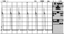
图4是图3中当输入电压处于高端时的同步整流管的驱动电压波形图。FIG. 4 is a waveform diagram of the drive voltage of the synchronous rectifier when the input voltage is at the high end in FIG. 3 .
具体实施方式Detailed ways
为了使本实用新型的目的、技术方案及优点更加清楚明白,以下结合附图及实施例,对本实用新型进行进一步详细说明。应当理解,此处所描述的具体实施例仅仅用以解释本实用新型,并不用于限定本实用新型。In order to make the purpose, technical solution and advantages of the utility model clearer, the utility model will be further described in detail below in conjunction with the accompanying drawings and embodiments. It should be understood that the specific embodiments described here are only used to explain the utility model, and are not intended to limit the utility model.
参考图3所示,本实用新型公开了一种同步整流驱动电路,其用于对同步整流电路进行驱动,与主变压器副边主绕组Ns相连,其包括驱动单元1、运放控制电路2及信号检测电路3,其中:Referring to Fig. 3, the utility model discloses a synchronous rectification drive circuit, which is used to drive the synchronous rectification circuit, and is connected with the main winding Ns on the secondary side of the main transformer, which includes a
在本实施例中,整流电路包括有同步整流管U1、同步续流管U2。In this embodiment, the rectification circuit includes a synchronous rectifier U1 and a synchronous freewheel U2.
驱动单元1包括两驱动电容C1、C2、两电阻R1、R2及两MOS管Q1、Q2;其中,两MOS管Q1、Q2为N沟道MOS管,其D极分别连接到主变压器副边主绕组Ns的同名端和异名端,其S极分别通过电阻R1、R2连接到同步整流管U1和同步续流管U2的G极,网络DRV1和DRV2分别代表两MOS管Q1、Q2的G极,并通过缓冲电路与运放控制电路2的输出端相连;两电容C1、C2分别并联于两MOS管Q1、Q2的DS之间。The
运放控制电路2包括六个电阻R11、R12、R13、R14、R15、R16、两个电容C6、C7及两个比较器U3-A、U3-B,其中:The operational
电阻R11的两端跨接在比较器U3-A的同相输入和输出端,电阻R14的一端与比较器U3-A的输出相连,电阻R14的另一端与第一个MOS的G极相连,电阻R12的两端跨接在比较器U3-B的同相输入和输出端,电阻R15的一端与比较器U3-B的输出端相连,另一端与第二个MOS的G极相连,电容C6的一端与第一个MOS的G极相连,另一端连接到地,电容C7的一端与第二个MOS的G极相连,另一端连接到地。电阻R13的一端与开关变换器的输出端相连,另一端与电阻R16及比较器U3-A的输入端相连,电阻R16的另一端接地。The two ends of the resistor R11 are connected across the non-inverting input and output terminals of the comparator U3-A, one end of the resistor R14 is connected to the output of the comparator U3-A, and the other end of the resistor R14 is connected to the G pole of the first MOS. The two ends of R12 are connected across the non-inverting input and output ends of the comparator U3-B, one end of the resistor R15 is connected to the output end of the comparator U3-B, the other end is connected to the G pole of the second MOS, and one end of the capacitor C6 It is connected to the G pole of the first MOS, and the other end is connected to the ground. One end of the capacitor C7 is connected to the G pole of the second MOS, and the other end is connected to the ground. One end of the resistor R13 is connected to the output end of the switching converter, the other end is connected to the resistor R16 and the input end of the comparator U3-A, and the other end of the resistor R16 is grounded.
实际应用中,比较器U3-A用做反相迟滞比较器,比较器U3-B用做同相迟滞比较器,电阻R11与电阻R12分别为比较器U3-A、U3-B的回差电阻,分别跨接与比较器U3-A、U3-B的输出与同相输入端,电阻R14、R15和电容C6、C7分为比较器U3-A、U3-B输出的缓冲电阻和缓冲电容,经过缓冲后分别与MOS管Q1、Q2的G极相连,比较器U3的3脚与6脚相连,V0为开关变换器的输出端,V0经电阻R13、R16分压后,作为参考电压,与比较器U3的3脚相连。In practical applications, the comparator U3-A is used as an inverting hysteresis comparator, and the comparator U3-B is used as a non-inverting hysteresis comparator. The resistors R11 and R12 are the hysteresis resistors of the comparators U3-A and U3-B respectively. Respectively across the output and non-inverting input terminals of comparators U3-A and U3-B, resistors R14, R15 and capacitors C6 and C7 are divided into buffer resistors and buffer capacitors output by comparators U3-A and U3-B, after buffering After that, they are respectively connected to the G poles of the MOS transistors Q1 and Q2, the 3rd pin of the comparator U3 is connected to the 6th pin, and V0 is the output terminal of the switching converter. The 3 pins of U3 are connected.
信号检测电路3包括一个二极管D1、四个电阻R7、R8、R9、R10、一个电容C5和一个稳压管Z1,其中:The signal detection circuit 3 includes a diode D1, four resistors R7, R8, R9, R10, a capacitor C5 and a voltage regulator tube Z1, wherein:
二极管D1、电阻R7及电容C5构成整流滤波电路,整流二极管D1的阳极与主变压器副边主绕组Ns的同名端相连,阴极与电阻R7的一端相连,电阻R7的另一端与电容C5的一端和电阻R8的一端相连;电容C5的另一端连接到地;电阻R8的另一端连接到稳压管Z1的阴极和运放控制电路2的比较器U3-B的同相输入端,稳压管Z1的阳极连接到地,电阻R9的一端连接到稳压管Z1的阴极,另一端连接到电阻R10的一端和运放控制电路2的比较器U3-A的反相输入端;电阻R10的另一端连接到地。Diode D1, resistor R7 and capacitor C5 form a rectification filter circuit. The anode of rectifier diode D1 is connected to the end of the same name of the main winding Ns on the secondary side of the main transformer, the cathode is connected to one end of resistor R7, and the other end of resistor R7 is connected to one end of capacitor C5 and One end of the resistor R8 is connected; the other end of the capacitor C5 is connected to the ground; the other end of the resistor R8 is connected to the cathode of the voltage regulator tube Z1 and the non-inverting input terminal of the comparator U3-B of the operational
整流滤波后的电压经电阻R8、R9、R10串联分压后,在电阻R9与电阻R10的连接点与比较器U3-A的反相输入端相连,在电阻R8、R9的连接点与比较器U3-B的同相输入端相连,同时,稳压管Z1的阴极也连接在电阻R8与电阻R9的连接点上,稳压管Z1的阳极连接到地,起到限幅作用。After the rectified and filtered voltage is divided in series by resistors R8, R9, and R10, it is connected to the inverting input terminal of comparator U3-A at the connection point of resistor R9 and resistor R10, and connected to the comparator at the connection point of resistors R8 and R9. The non-inverting input terminal of U3-B is connected, and at the same time, the cathode of the voltage regulator tube Z1 is also connected to the connection point of the resistor R8 and the resistor R9, and the anode of the voltage regulator tube Z1 is connected to the ground, which acts as a limiter.
本领域的普通技术人员明白,对于宽范围4∶1的输入电压范围,采用绕组自驱时,低压占空比较大,高压占空比较小,同步整流管的驱动电压幅值在低压时最小,高压时最大,而同步续流管的驱动电压幅值刚好相反,即低压时最大,高压时最小,因此,控制MOS管Q1通断的比较器U3-A需采用反相输入,而控制MOS管Q2通断的比较器U3-B需采用同相输入,两者互补。Those of ordinary skill in the art understand that for a wide range of 4:1 input voltage range, when the winding self-drive is used, the low-voltage duty ratio is large, and the high-voltage duty ratio is small, and the driving voltage amplitude of the synchronous rectifier is the smallest at low voltage. It is the largest at high voltage, and the driving voltage amplitude of the synchronous freewheeling tube is just the opposite, that is, the largest at low voltage and the smallest at high voltage. Therefore, the comparator U3-A that controls the on-off of the MOS transistor Q1 needs to use an inverting input, while the control MOS transistor Q1 The comparator U3-B for Q2 on-off needs to use the non-inverting input, and the two are complementary.
当输入电压处于18V时,同步整流管U1的驱动电压幅值最小,而同步续流管U2的驱动电压幅值最大,此时,主变压器副边主绕组Ns同名端的电压也较低,经采样分压送至比较器U3-A的反相输入电压也较低,低于比较器U3-A的同相输入的参考电压时,U3-A的输出脚为高电平,进而MOS管Q1导通,同步整流管U1的驱动电压直接来主变压器副边主绕组Ns的同名端的电压,并经同步整流管U1的GS电容回到主变压器副边主绕组Ns异名端,弥补低压时,同步整流管U1的驱动电压幅值较低的现象。比较器U3-B的同相输入电压低于反相输入的参考电压,比较器U3-B的输出脚为低电平,MOS管Q2不导通,主变压器副边主绕组Ns的异名端电压经电容C2和同步续流管U2的GS间的电容分压,并经同步续流管U2的GS电容回到主变压器副边主绕组Ns同名端,弥补低压时,同步续流管U2的驱动电压幅值较高的现象,值得注意的是,当MOS管Q1或Q2没有导通时,其体内二极管为电容C1或C2提供了放电通路,避免了额外增加放电回路的问题。When the input voltage is 18V, the driving voltage amplitude of the synchronous rectifier tube U1 is the smallest, and the driving voltage amplitude of the synchronous freewheeling tube U2 is the largest. The inverting input voltage sent to the comparator U3-A by dividing the voltage is also low. When it is lower than the reference voltage of the non-inverting input of the comparator U3-A, the output pin of U3-A is at a high level, and the MOS transistor Q1 is turned on. , the driving voltage of the synchronous rectifier U1 directly comes from the voltage of the same-named end of the main winding Ns on the secondary side of the main transformer, and returns to the different-named end of the main winding Ns on the secondary side of the main transformer through the GS capacitor of the synchronous rectifier U1, to compensate for low voltage, synchronous rectification The phenomenon that the driving voltage amplitude of the tube U1 is low. The non-inverting input voltage of the comparator U3-B is lower than the reference voltage of the inverting input, the output pin of the comparator U3-B is low level, the MOS transistor Q2 is not turned on, and the voltage of the non-identical terminal of the main winding Ns on the secondary side of the main transformer Divide the voltage between the capacitor C2 and the GS of the synchronous freewheeling tube U2, and return to the same-named terminal of the main winding Ns on the secondary side of the main transformer through the GS capacitor of the synchronous freewheeling tube U2 to make up for the drive of the synchronous freewheeling tube U2 at low voltage For the phenomenon of high voltage amplitude, it is worth noting that when the MOS transistor Q1 or Q2 is not turned on, its body diode provides a discharge path for the capacitor C1 or C2, avoiding the problem of adding an additional discharge circuit.
当输入电压处于72V时,比较器U3-A、U3-B的输出端电平与输入电压处于18V时的电平刚好相反,即比较器U3-A的输出脚为低电平,比较器U3-B的输出脚为高电平,此时驱动电路的工作原理同上,从而弥补了高压时,同步整流管U1的驱动电压幅值较高与同步续洲管U2的驱动电压幅值较低的现象。When the input voltage is 72V, the output levels of the comparators U3-A and U3-B are just opposite to those when the input voltage is 18V, that is, the output pin of the comparator U3-A is at low level, and the comparator U3 The output pin of -B is at high level, and the working principle of the driving circuit is the same as above at this time, so as to make up for the high voltage amplitude of the synchronous rectifier U1 and the low driving voltage amplitude of the synchronous rectifier U2 at high voltage. Phenomenon.
MOS管Q1、Q2何时导通与关断可以根据电路实际应用情况对电路参数做出调整,具体可以调整运放控制单元电路和信号检测单元电路。通过合理的调整,可以使同步整流管和同步续流的驱动电压的幅值在整个输入电压范围内控制在一个合适的范围,且不影响驱动电压的上升或下降斜率,同时MOS管Q1、Q2的体内二极管也得到了合理的利用,因此,驱动损耗在整个输入电压范围内都相对较小,驱动电路中器件的封装可选用小型号的封装,驱动性能较好,从而提高了开关变换器的效率。When the MOS transistors Q1 and Q2 are turned on and off can adjust the circuit parameters according to the actual application of the circuit. Specifically, the operational amplifier control unit circuit and the signal detection unit circuit can be adjusted. Through reasonable adjustment, the driving voltage amplitude of the synchronous rectifier and synchronous freewheeling can be controlled in an appropriate range within the entire input voltage range without affecting the rising or falling slope of the driving voltage. At the same time, the MOS transistors Q1 and Q2 The diode in the body has also been reasonably utilized, so the drive loss is relatively small in the entire input voltage range, and the package of the device in the drive circuit can be a small package, and the drive performance is better, thereby improving the switching converter. efficiency.
本实用新型也可在应用中根据具体的输出电压和匝比关系,用独立绕组的同名端来做采样电压,使采样电压在全电压输入范围内达到一合适的幅值,并非必须采用直接取自主变压器T1副边主绕组Ns的同名端来实现。而同步整流管和同步续流管的驱动电路也可单独应用,并且参考电压也可以通其它辅助电源经稳压后得到,以使该同步整流驱动电路获得满意的性能。The utility model can also use the end of the same name of the independent winding to make the sampling voltage according to the specific output voltage and the turn ratio relationship in the application, so that the sampling voltage can reach a suitable amplitude within the full voltage input range, and it is not necessary to directly take the It is realized by the terminal with the same name of the main winding Ns on the secondary side of the main transformer T1. The driving circuit of the synchronous rectifier and the synchronous freewheeling tube can also be used separately, and the reference voltage can also be obtained after being stabilized by other auxiliary power sources, so that the synchronous rectification driving circuit can obtain satisfactory performance.
由图4可见,本实用新型采用上述技术方案后,通过控制MOS管的导通与关断,实现了驱动电容与MOS管的分段驱动,输入电压范围可以扩大到4∶1,甚至更宽,更重要的是使同步整流管和同步续流管驱动电压的幅值在整个输入电压范围内得到合理分配,避免了同步整流管或同步续流管的损坏,降低了驱动电路带来的损耗,提高了整机的效率,并且,结构相对简单,效率高,通用性强,便于广泛应用。It can be seen from Figure 4 that after the utility model adopts the above-mentioned technical solution, by controlling the on and off of the MOS tube, the segmental drive of the driving capacitor and the MOS tube is realized, and the input voltage range can be expanded to 4:1, or even wider , the more important thing is to make the driving voltage amplitude of synchronous rectifier and synchronous freewheeling tube be reasonably distributed in the whole input voltage range, avoiding the damage of synchronous rectifier or synchronous freewheeling tube, and reducing the loss caused by the driving circuit , improves the efficiency of the whole machine, and has a relatively simple structure, high efficiency, strong versatility, and is convenient for wide application.
同时,同步整流管和同步续流管的驱动电压上升斜率较大,避免了同步整流管和同步续流管的体内二极管导通时间过长造成额外的损耗;当驱动电压较高时,MOS处于关断时,驱动电压通过驱动电容及同步管的GS间的电容分压,从而使驱动电压的幅值降低,此时,巧妙地利用了MOS的体内二极管给驱动电容放电,节省了额外增加放电二极管,而当驱动电压较低时,MOS导通,此时将驱动电容短路,驱动电压通过一电阻加到同步管的GS间,从而使驱动电压的幅值提高,而这个电阻提高了驱动电路的阻尼系数,可有效抑驱动电压中有变压器漏感产生的电压尖峰。无论MOS管是否导通,驱动电压的波形都没有发生改变,且幅值保持在合适的范围,不但使驱动电路本身的损耗减小,也使同步整流管和同步续流管的导通损耗降低,从而提高了开关变换器的效率;在两比较器的输出端分别设有缓冲电路,这是为了提高MOS管导通的速率。原因是MOS管在开通的瞬间会遇到两种情况,即MOS管的体内二极管是否处于放电导通状态,通过设置缓冲电路,无论处于哪种状态都可以使MOS迅速导通,所以在转换的过程中对输出波形没有任何影响。At the same time, the rising slope of the driving voltage of the synchronous rectifier and the synchronous freewheeling tube is relatively large, which avoids the extra loss caused by the long conduction time of the internal diode of the synchronous rectifier and the synchronous freewheeling tube; when the driving voltage is high, the MOS is in the When it is turned off, the driving voltage is divided by the capacitance between the driving capacitor and the GS of the synchronous tube, so that the amplitude of the driving voltage is reduced. At this time, the internal diode of the MOS is cleverly used to discharge the driving capacitor, saving additional discharge Diode, and when the driving voltage is low, the MOS is turned on. At this time, the driving capacitor is short-circuited, and the driving voltage is added to the GS of the synchronous tube through a resistor, so that the amplitude of the driving voltage is increased, and this resistance improves the driving circuit. The damping coefficient can effectively suppress the voltage spike generated by the transformer leakage inductance in the driving voltage. Regardless of whether the MOS tube is turned on or not, the waveform of the driving voltage does not change, and the amplitude remains in an appropriate range, which not only reduces the loss of the driving circuit itself, but also reduces the conduction loss of the synchronous rectifier tube and the synchronous freewheeling tube. , thus improving the efficiency of the switching converter; the output terminals of the two comparators are respectively equipped with buffer circuits, which is to increase the turn-on rate of the MOS tube. The reason is that the MOS tube will encounter two situations at the moment when it is turned on, that is, whether the body diode of the MOS tube is in the discharge and conduction state. By setting the buffer circuit, no matter which state it is in, the MOS can be quickly turned on. The process has no effect on the output waveform.
由此可见,本实用新型可有效地解决当输入电压范围较宽时,自驱动电路中同步整流管和同步续流管驱动电压的幅值受到输入电压变化范围限制的不足,使同步整流管和同步续流管驱动电压的幅值在整个输入电压范围内得到合理分配,避免了同步整流管或同步续流管的损坏,降低了驱动电路带来的损耗,提高了整机的效率,并且,结构相对简单,成本低,效率高,通用性强,特别适合于各种宽范围输入的中、小功率开关变换器副边的同步整流的驱动。It can be seen that the utility model can effectively solve the problem that the amplitude of the driving voltage of the synchronous rectifier and the synchronous freewheeling tube in the self-driving circuit is limited by the variation range of the input voltage when the input voltage range is wide, so that the synchronous rectifier and the synchronous rectifier The amplitude of the driving voltage of the synchronous freewheeling tube is reasonably distributed within the entire input voltage range, avoiding the damage of the synchronous rectifying tube or the synchronous freewheeling tube, reducing the loss caused by the driving circuit, and improving the efficiency of the whole machine, and, The structure is relatively simple, the cost is low, the efficiency is high, and the versatility is strong, which is especially suitable for driving the synchronous rectification of the secondary side of the medium and small power switching converters with various wide-range inputs.
以上所述,仅为本实用新型较佳的具体实施方式,但本实用新型的保护范围并不局限于此,任何熟悉本技术领域的技术人员在本实用新型揭露的技术范围内,可轻易想到的变化或替换,都应涵盖在本实用新型的保护范围之内。因此,本实用新型的保护范围应该以权利要求的保护范围为准。The above is only a preferred embodiment of the utility model, but the scope of protection of the utility model is not limited thereto, and any person familiar with the technical field can easily think of All changes or replacements should fall within the protection scope of the present utility model. Therefore, the protection scope of the present utility model should be based on the protection scope of the claims.
Claims (5)
Priority Applications (1)
| Application Number | Priority Date | Filing Date | Title |
|---|---|---|---|
| CN2011204930656UCN202424561U (en) | 2011-12-01 | 2011-12-01 | Synchronous rectification driving circuit |
Applications Claiming Priority (1)
| Application Number | Priority Date | Filing Date | Title |
|---|---|---|---|
| CN2011204930656UCN202424561U (en) | 2011-12-01 | 2011-12-01 | Synchronous rectification driving circuit |
Publications (1)
| Publication Number | Publication Date |
|---|---|
| CN202424561Utrue CN202424561U (en) | 2012-09-05 |
Family
ID=46749284
Family Applications (1)
| Application Number | Title | Priority Date | Filing Date |
|---|---|---|---|
| CN2011204930656UExpired - Fee RelatedCN202424561U (en) | 2011-12-01 | 2011-12-01 | Synchronous rectification driving circuit |
Country Status (1)
| Country | Link |
|---|---|
| CN (1) | CN202424561U (en) |
Cited By (3)
| Publication number | Priority date | Publication date | Assignee | Title |
|---|---|---|---|---|
| CN105846700A (en)* | 2016-03-29 | 2016-08-10 | 广州视源电子科技股份有限公司 | LLC half-bridge resonant converter and secondary synchronous rectifying device thereof |
| CN110932574A (en)* | 2019-12-23 | 2020-03-27 | 中国电子科技集团公司第四十三研究所 | A miniaturized and highly reliable self-driven synchronous rectifier circuit |
| CN111564959A (en)* | 2019-10-16 | 2020-08-21 | 成都芯源系统有限公司 | Power driving circuit suitable for switching converter |
- 2011
- 2011-12-01CNCN2011204930656Upatent/CN202424561U/ennot_activeExpired - Fee Related
Cited By (4)
| Publication number | Priority date | Publication date | Assignee | Title |
|---|---|---|---|---|
| CN105846700A (en)* | 2016-03-29 | 2016-08-10 | 广州视源电子科技股份有限公司 | LLC half-bridge resonant converter and secondary synchronous rectifying device thereof |
| CN111564959A (en)* | 2019-10-16 | 2020-08-21 | 成都芯源系统有限公司 | Power driving circuit suitable for switching converter |
| CN111564959B (en)* | 2019-10-16 | 2023-10-17 | 成都芯源系统有限公司 | Power driving circuit suitable for switching converter |
| CN110932574A (en)* | 2019-12-23 | 2020-03-27 | 中国电子科技集团公司第四十三研究所 | A miniaturized and highly reliable self-driven synchronous rectifier circuit |
Similar Documents
| Publication | Publication Date | Title |
|---|---|---|
| CN110611431B (en) | Primary side regulation control system and control method of active clamp flyback converter | |
| CN103424602B (en) | Based on the secondary winding current testing circuit of source drive | |
| CN202759383U (en) | Switch power supply with high power factor | |
| CN106793339B (en) | Adaptive line voltage compensation LED drive circuit based on primary side feedback | |
| CN103269161B (en) | Constant-current output BUCK power circuit | |
| CN203814013U (en) | LED driving circuit adopting single-end zero crossing detection | |
| CN203167339U (en) | A LED driving circuit without auxiliary winding | |
| CN105407583B (en) | Single-pole quasi-resonance LED driving device based on Buck-Boost circuit and Flyback circuit | |
| CN203537225U (en) | Novel antisurge constant-current switching power supply | |
| CN103298215B (en) | Control circuit of flyback LED (Light Emitting Diode) driver | |
| CN102480221A (en) | Application method of PFC (power factor correction) controller in Buck circuit | |
| CN101924483A (en) | Voltage doubler synchronous rectification circuit with energy recovery | |
| CN202424561U (en) | Synchronous rectification driving circuit | |
| CN201656780U (en) | Auxiliary source circuit applicable to switch power supply | |
| CN201113788Y (en) | A power protection circuit | |
| CN202759634U (en) | LED drive circuit without auxiliary winding | |
| CN201928486U (en) | Pulse width modulation (PWM) dimming light-emitting diode (LED) driving circuit | |
| CN207664888U (en) | High efficiency full bridge rectifier | |
| CN104022672B (en) | Self adaptation adjustable delay circuit for Sofe Switch ZVT changer | |
| CN203352471U (en) | Photovoltaic inverter-used single end flyback-type switching power supply primary-side circuit | |
| CN103312131A (en) | High-frequency direct-current converter switch tube turn-off speed real-time adjustment method | |
| CN202190220U (en) | Synchronous rectification circuit | |
| CN106413202B (en) | Primary side control L ED drive circuit based on SEPIC and Flyback circuit | |
| CN209329979U (en) | Air-cooled radar transmitter high-power AC-DC constant current power supply circuit and power supply device | |
| CN201550024U (en) | Double transistor forward high voltage DC electricity getting unit with neutral points |
Legal Events
| Date | Code | Title | Description |
|---|---|---|---|
| C14 | Grant of patent or utility model | ||
| GR01 | Patent grant | ||
| CF01 | Termination of patent right due to non-payment of annual fee | Granted publication date:20120905 Termination date:20161201 | |
| CF01 | Termination of patent right due to non-payment of annual fee |