CN202308030U - Structure improvement of multi-layer array type LED light engine - Google Patents
Structure improvement of multi-layer array type LED light engineDownload PDFInfo
- Publication number
- CN202308030U CN202308030UCN2011203081318UCN201120308131UCN202308030UCN 202308030 UCN202308030 UCN 202308030UCN 2011203081318 UCN2011203081318 UCN 2011203081318UCN 201120308131 UCN201120308131 UCN 201120308131UCN 202308030 UCN202308030 UCN 202308030U
- Authority
- CN
- China
- Prior art keywords
- light engine
- structural improvement
- led light
- layer
- layer array
- Prior art date
- Legal status (The legal status is an assumption and is not a legal conclusion. Google has not performed a legal analysis and makes no representation as to the accuracy of the status listed.)
- Expired - Fee Related
Links
- 230000002093peripheral effectEffects0.000claimsabstractdescription20
- 239000005022packaging materialSubstances0.000claimsabstractdescription18
- 239000000463materialSubstances0.000claimsabstractdescription16
- 238000005538encapsulationMethods0.000claimsabstractdescription5
- 239000010410layerSubstances0.000claimsdescription83
- 239000000758substrateSubstances0.000claimsdescription59
- 238000004806packaging method and processMethods0.000claimsdescription27
- 230000003287optical effectEffects0.000claimsdescription25
- 239000013078crystalSubstances0.000claimsdescription16
- 238000002955isolationMethods0.000claimsdescription14
- VYPSYNLAJGMNEJ-UHFFFAOYSA-NSilicium dioxideChemical compoundO=[Si]=OVYPSYNLAJGMNEJ-UHFFFAOYSA-N0.000claimsdescription13
- 229920005989resinPolymers0.000claimsdescription13
- 239000011347resinSubstances0.000claimsdescription13
- 239000000741silica gelSubstances0.000claimsdescription13
- 229910002027silica gelInorganic materials0.000claimsdescription13
- 229910000679solderInorganic materials0.000claimsdescription7
- 238000000465mouldingMethods0.000claimsdescription6
- 239000003292glueSubstances0.000claimsdescription5
- 239000012790adhesive layerSubstances0.000claimsdescription4
- 239000007767bonding agentSubstances0.000claimsdescription4
- 229920006375polyphtalamidePolymers0.000claimsdescription4
- 229920001296polysiloxanePolymers0.000claimsdescription4
- 229920000106Liquid crystal polymerPolymers0.000claimsdescription3
- 239000004954PolyphthalamideSubstances0.000claimsdescription3
- 239000011241protective layerSubstances0.000claimsdescription3
- 230000004308accommodationEffects0.000claimsdescription2
- 239000003822epoxy resinSubstances0.000claimsdescription2
- 229920000647polyepoxidePolymers0.000claimsdescription2
- 239000004977Liquid-crystal polymers (LCPs)Substances0.000claims1
- 238000000748compression mouldingMethods0.000claims1
- 239000007788liquidSubstances0.000abstractdescription8
- 238000007711solidificationMethods0.000abstractdescription2
- 230000008023solidificationEffects0.000abstractdescription2
- 230000003746surface roughnessEffects0.000abstractdescription2
- 239000011230binding agentSubstances0.000abstract1
- 238000005476solderingMethods0.000abstract1
- 238000010586diagramMethods0.000description17
- 239000004033plasticSubstances0.000description9
- 239000010432diamondSubstances0.000description5
- 229910003460diamondInorganic materials0.000description5
- 229910052751metalInorganic materials0.000description5
- 239000002184metalSubstances0.000description5
- 239000007787solidSubstances0.000description4
- 239000011344liquid materialSubstances0.000description3
- 239000000843powderSubstances0.000description3
- 238000007789sealingMethods0.000description3
- XLYOFNOQVPJJNP-UHFFFAOYSA-NwaterChemical compoundOXLYOFNOQVPJJNP-UHFFFAOYSA-N0.000description3
- PXHVJJICTQNCMI-UHFFFAOYSA-NNickelChemical compound[Ni]PXHVJJICTQNCMI-UHFFFAOYSA-N0.000description2
- BQCADISMDOOEFD-UHFFFAOYSA-NSilverChemical compound[Ag]BQCADISMDOOEFD-UHFFFAOYSA-N0.000description2
- 230000004048modificationEffects0.000description2
- 238000012986modificationMethods0.000description2
- 239000004065semiconductorSubstances0.000description2
- 229910052709silverInorganic materials0.000description2
- 239000004332silverSubstances0.000description2
- OKTJSMMVPCPJKN-UHFFFAOYSA-NCarbonChemical compound[C]OKTJSMMVPCPJKN-UHFFFAOYSA-N0.000description1
- ATJFFYVFTNAWJD-UHFFFAOYSA-NTinChemical compound[Sn]ATJFFYVFTNAWJD-UHFFFAOYSA-N0.000description1
- 229910052799carbonInorganic materials0.000description1
- 239000003086colorantSubstances0.000description1
- 230000006866deteriorationEffects0.000description1
- 230000000694effectsEffects0.000description1
- 230000008571general functionEffects0.000description1
- 238000009434installationMethods0.000description1
- QSHDDOUJBYECFT-UHFFFAOYSA-NmercuryChemical compound[Hg]QSHDDOUJBYECFT-UHFFFAOYSA-N0.000description1
- 229910052753mercuryInorganic materials0.000description1
- 239000007769metal materialSubstances0.000description1
- 238000000034methodMethods0.000description1
- 239000000203mixtureSubstances0.000description1
- 229910052759nickelInorganic materials0.000description1
- 230000000149penetrating effectEffects0.000description1
- 239000000126substanceSubstances0.000description1
Images


Classifications
- H—ELECTRICITY
- H01—ELECTRIC ELEMENTS
- H01L—SEMICONDUCTOR DEVICES NOT COVERED BY CLASS H10
- H01L2224/00—Indexing scheme for arrangements for connecting or disconnecting semiconductor or solid-state bodies and methods related thereto as covered by H01L24/00
- H01L2224/01—Means for bonding being attached to, or being formed on, the surface to be connected, e.g. chip-to-package, die-attach, "first-level" interconnects; Manufacturing methods related thereto
- H01L2224/42—Wire connectors; Manufacturing methods related thereto
- H01L2224/47—Structure, shape, material or disposition of the wire connectors after the connecting process
- H01L2224/48—Structure, shape, material or disposition of the wire connectors after the connecting process of an individual wire connector
- H01L2224/4805—Shape
- H01L2224/4809—Loop shape
- H01L2224/48091—Arched
- H—ELECTRICITY
- H01—ELECTRIC ELEMENTS
- H01L—SEMICONDUCTOR DEVICES NOT COVERED BY CLASS H10
- H01L2224/00—Indexing scheme for arrangements for connecting or disconnecting semiconductor or solid-state bodies and methods related thereto as covered by H01L24/00
- H01L2224/01—Means for bonding being attached to, or being formed on, the surface to be connected, e.g. chip-to-package, die-attach, "first-level" interconnects; Manufacturing methods related thereto
- H01L2224/42—Wire connectors; Manufacturing methods related thereto
- H01L2224/47—Structure, shape, material or disposition of the wire connectors after the connecting process
- H01L2224/48—Structure, shape, material or disposition of the wire connectors after the connecting process of an individual wire connector
- H01L2224/481—Disposition
- H01L2224/48135—Connecting between different semiconductor or solid-state bodies, i.e. chip-to-chip
- H01L2224/48137—Connecting between different semiconductor or solid-state bodies, i.e. chip-to-chip the bodies being arranged next to each other, e.g. on a common substrate
Landscapes
- Led Device Packages (AREA)
Abstract
Description
Translated fromChinese技术领域technical field
一种发光二极管光引擎的结构改良,尤其是一种完全阻绝水气进入、坚固耐用及长期维持光学组件效能的一种高强度气密型多层式阵列型发光二极管的封装结构改良。A structural improvement of a light-emitting diode light engine, especially a high-strength airtight multilayer array-type light-emitting diode packaging structure improvement that completely prevents water vapor from entering, is durable, and maintains the performance of optical components for a long time.
背景技术Background technique
按LED的发光原理是利用半导体固有特性,它不同于以往的白炽灯管的放电、发热发光原理,而是将电流顺向流入半导体的PN接面时便会发出光线,所以LED被称为冷光源(cold light)。由于LED具有高耐久性、寿命长、轻巧、耗电量低且不含水银等有害物质等的优点,故可广泛应用于照明设备产业中,且其通常以LED阵列封装方式应用在电子广告牌、交通号志等商业领域。According to the light-emitting principle of LED, it uses the inherent characteristics of semiconductors. It is different from the discharge and heat-emitting principles of incandescent tubes in the past. Instead, it emits light when the current flows into the PN junction of the semiconductor in the forward direction, so LED is called cold. light source (cold light). Due to the advantages of high durability, long life, light weight, low power consumption and no harmful substances such as mercury, LEDs can be widely used in the lighting equipment industry, and they are usually used in electronic billboards in the form of LED array packaging. , traffic signals and other commercial fields.
请参考新型专利公告号M393044的申请案的应用于发光二极管封装结构的具有荧光层的光学透镜,在此仅作一般功能的描述。参考图1,应用于发光二极管封装结构的具有荧光层的光学透镜的剖视图,其包含基板1a、封装体2a、导线架3a、光学透镜4a及透镜罩5a,基板1a位于封装结构的最底层部分,其中基板1a的各面皆形状平整且光滑的面,该基板1a的周边部分会被该封装体1a包覆固定,封装体2a的内壁面并设置有光学反射罩6a,封装体2a并也包覆固定导线架3a,导线架3a的各面皆形状亦为平整且光滑的面。Please refer to the application of New Patent Publication No. M393044 for an optical lens with a fluorescent layer applied to a light-emitting diode packaging structure, which is only described here for general functions. Referring to FIG. 1 , a cross-sectional view of an optical lens with a fluorescent layer applied to a light-emitting diode packaging structure, which includes a substrate 1a, a
光学反射罩6a上配置有光学透镜4a及透镜罩5a,其中透镜罩5a覆盖住光学透镜4a,透镜罩5a藉由黏合方式固定在光学反射罩6a的顶部,以及使透镜罩5a嵌合于封装体2a之中,以使透镜罩5a可紧密固定于封装体2a及光学反射罩6a上。An
然而现有技术的缺点在于由于基板的各面是平滑的表面,当封装体将基板封装固定后,会形成一种平面对平面的接触关系,由于平面对平面的接触,使得封装体与基板相互间的摩擦力很少,导致会产生滑动不稳固的情形,此种滑动不稳固的情形也发生于导线架上,且封装体通常是使用液态状的材料包覆在基板或其它欲封装的构件的周围,当液态状的材料固态化以将基板封装起来,但是当基板的各面过于平滑,将难以使液态状的材料平均性的布满于基板各面,此种情形的解决方式,不外乎是增加材料用量或以人工方式去处理,相当耗损成本。However, the disadvantage of the prior art is that since each surface of the substrate is a smooth surface, when the package fixes the substrate, a plane-to-plane contact relationship will be formed. Due to the plane-to-plane contact, the package and the substrate are mutually There is very little friction between them, resulting in unstable sliding, which also occurs on the lead frame, and the package is usually covered with a liquid material on the substrate or other components to be packaged around, when the liquid material is solidified to encapsulate the substrate, but when the surfaces of the substrate are too smooth, it will be difficult to make the liquid material uniformly spread on all surfaces of the substrate. The solution to this situation is not It is nothing more than increasing the amount of materials or handling them manually, which consumes a lot of cost.
现有技术的另一缺点还有透镜罩难以长期固定于光学反射罩上,因为透镜罩的材质是塑料材质,而光学反射罩为了使光线反射高提高,会选用金属材质或在表面上镀上一层金属薄膜,但由于塑料不易与金属的表面接着固定,导致塑料材质的透镜罩会慢慢地脱离于金属材质的光学反射罩。Another shortcoming of the prior art is that the lens cover is difficult to fix on the optical reflector for a long time, because the material of the lens cover is plastic material, and the optical reflector will use metal material or plate it on the surface in order to improve the light reflection. A layer of metal film, but because the plastic is not easy to be fixed with the metal surface, the plastic lens cover will slowly separate from the metal optical reflector.
当基板与封装体发生松动的状况,以及透镜罩无法紧密地固定于光学反射镜时,将导致湿气或水气容易渗入于封装结构内部,导致发光组件及光学单元劣化甚至损毁,因此无法使用于潮湿的环境下,因此必须对此加以改良,并提供一种完全阻绝水气进入、并坚固耐用及长期维持光学组件效能的一种发光二极管的封装结构。When the substrate and package are loose, and the lens cover cannot be tightly fixed to the optical mirror, moisture or water vapor will easily penetrate into the package structure, resulting in deterioration or even damage to the light-emitting component and optical unit, so it cannot be used In a humid environment, it is necessary to improve this, and provide a package structure of light-emitting diodes that completely prevents the entry of water vapor, is durable, and maintains the performance of optical components for a long time.
实用新型内容Utility model content
本实用新型的主要目的在于提供一种多层式阵列型发光二极管光引擎的结构改良,其中基板的周边区块的各面上形成有一表面结构,该表面结构为凹陷部与凸出部相互交隔间错的态样,凹陷部可使液态状态的封装材料填流于表面结构的凹陷部,当封装材料固态化后,封装材料填流于凹陷部的部分以及封装材料对应于凸出部的部分皆与基板形成卡合的关系,如此基板与封装材料固态后所形成的封装体会紧密地结合并固定成一体,进而大幅提升基板对封装体的结构强度及封装密合度。The main purpose of the present utility model is to provide a structural improvement of a multi-layer array type light-emitting diode light engine, wherein a surface structure is formed on each surface of the peripheral block of the substrate, and the surface structure is that the concave part and the protruding part intersect each other. In the case of compartmentalization, the concave part can make the liquid packaging material flow into the concave part of the surface structure. When the packaging material is solidified, the part of the packaging material that fills the concave part and the part of the packaging material corresponding to the protruding part Parts are engaged with the substrate, so that the package formed by the solid state of the substrate and the packaging material is tightly combined and fixed into one body, thereby greatly improving the structural strength of the substrate to the package and the packaging tightness.
为了达到上述目的,本实用新型中的一种多层式阵列型发光二极管光引擎的结构改良,包含有:In order to achieve the above purpose, the structural improvement of a multi-layer array type LED light engine in the present invention includes:
一基板,该基板可区分为一中心区及一周边区,该中心区的顶面为一出光面,该基板并具有一边缘,该中心区涵盖该基板的中间区块,该周边区为在该中心区与该边缘之间的区块,其中该周边区具有一顶面、一侧面及一底面,在该顶面形成有两容置槽;A substrate, the substrate can be divided into a central area and a peripheral area, the top surface of the central area is a light-emitting surface, and the substrate has an edge, the central area covers the middle area of the substrate, and the peripheral area is in the The block between the central area and the edge, wherein the peripheral area has a top surface, a side surface and a bottom surface, and two accommodation grooves are formed on the top surface;
一封装体,该封装体包覆该基板的该周边区部分但不包覆该中心区,该封装体的包覆区域包含有该顶面、该侧面及该底面,该封装体具有一封装腔室,该封装腔室位于该出光面之上;A package body, the package body covers the peripheral area part of the substrate but does not cover the central area, the package body covers the top surface, the side surface and the bottom surface, and the package body has a package cavity chamber, the encapsulation chamber is located on the light-emitting surface;
两导线架,该两导线架皆具有一内端部及一外端部,该两导线架的该内端部分别位于该两容置槽之中,该两导线架的该内端部及该外端部之间部分皆被封埋于该封装体之中,而该内端部及该外端部则露出于该封装体之外;以及Two lead frames, the two lead frames both have an inner end and an outer end, the inner ends of the two lead frames are respectively located in the two accommodating grooves, the inner ends of the two lead frames and the parts between the outer ends are embedded in the package, and the inner end and the outer end are exposed outside the package; and
多个发光二极管晶粒,所述发光二极管晶粒设置于该出光面,所述发光二极管晶粒与该两导线架构成电性连接关系。A plurality of LED crystal grains, the LED crystal grains are arranged on the light-emitting surface, and the LED crystal grains form an electrical connection relationship with the two lead frames.
其中,包覆于封装体中的导线架具有多个第二凹点,所述第二凹点可使液态状态的封装材料填流其中,避免液态状的封装材料从导线架流散出去,当封装材料固态化后,封装材料填流于所述第二凹点的部分会皆与导线架形成卡合的关系,如此导线架与封装材料固态后所形成的封装体会紧密地结合并固定成一体,进而提升导线架对封装体的接合度。Wherein, the lead frame wrapped in the package body has a plurality of second concave points, and the second concave points can fill the packaging material in the liquid state to prevent the liquid packaging material from flowing out from the lead frame. After the material is solidified, the portion of the packaging material that fills the second concave point will form an engaging relationship with the lead frame, so that the lead frame and the package formed after the packaging material is solid are tightly combined and fixed into one body, Further, the bonding degree of the lead frame to the package body is improved.
其中,设置在封装结构最上层的透镜底部可进一步涂布有结合剂,结合剂可使透镜更紧密地与其之下的构件相黏合,藉以阻绝外界湿气侵入于透镜内及封装结构的内部,且透镜浮设于与透镜材质相似的硅胶隔离层上,而非配置于光学反射罩上,进而防止透镜发生松动脱离的情形,且提升透镜在封装结构中的密合性。其中,利用掺杂钻石粉的焊膏,将发光二极管晶粒焊设于基板上,由于钻石粉具有较佳的导热效果,因此可有效将发光二极管晶粒产生的热能导出,其中钻石粉还可镀上具有导热性能优异的材质,如此发光二极管晶粒所产生的热能可被更快地排散至外部环境空间。Wherein, the bottom of the lens disposed on the uppermost layer of the packaging structure can be further coated with a bonding agent, which can make the lens more tightly bonded to the components below it, so as to prevent external moisture from intruding into the lens and the inside of the packaging structure, And the lens floats on the silicone isolation layer similar to the lens material, instead of being arranged on the optical reflector, thereby preventing the lens from loosening and detaching, and improving the tightness of the lens in the packaging structure. Among them, the LED crystal grains are soldered on the substrate by using solder paste doped with diamond powder. Since diamond powder has a better heat conduction effect, it can effectively export the heat energy generated by the LED crystal grains. The diamond powder can also The material with excellent thermal conductivity is plated, so that the heat energy generated by the light-emitting diode crystal grains can be dissipated to the external environment space more quickly.
附图说明Description of drawings
图1为现有技术的应用于发光二极管封装结构的具有荧光层的光学透镜的剖视图;1 is a cross-sectional view of an optical lens with a fluorescent layer applied to a light-emitting diode packaging structure in the prior art;
图2为本实用新型的多层式阵列型发光二极管光引擎的结构改良的第一实施例示意图;Fig. 2 is a schematic diagram of the first embodiment of the structural improvement of the multi-layer array type LED light engine of the present invention;
图3A为本实用新型的多层式阵列型发光二极管光引擎的结构改良的俯视示意图;FIG. 3A is a schematic top view of the structural improvement of the multi-layer array LED light engine of the present invention;
图3B为图2A的区域A的局部剖视放大图;FIG. 3B is an enlarged partial cross-sectional view of area A in FIG. 2A;
图4为本实用新型的多层式阵列型发光二极管光引擎的结构改良的第二实施例示意图;4 is a schematic diagram of a second embodiment of the structural improvement of the multi-layer array type LED light engine of the present invention;
图5为本实用新型的基板的第一实施例示意图;5 is a schematic diagram of a first embodiment of the substrate of the present invention;
图6为本实用新型的基板的第二实施例示意图;6 is a schematic diagram of a second embodiment of the substrate of the present invention;
图7为本实用新型的基板的第三实施例示意图;7 is a schematic diagram of a third embodiment of the substrate of the present invention;
图8为本实用新型的基板的第四实施例示意图;8 is a schematic diagram of a fourth embodiment of the substrate of the present invention;
图9为本实用新型的基板的第五实施例示意图;9 is a schematic diagram of a fifth embodiment of the substrate of the present invention;
图10为本实用新型的基板的第六实施例示意图;10 is a schematic diagram of a sixth embodiment of the substrate of the present invention;
图11为本实用新型的多层式阵列型发光二极管光引擎的结构改良的较佳实施例示意图;FIG. 11 is a schematic diagram of a preferred embodiment of the structural improvement of the multi-layer array type LED light engine of the present invention;
图12A为图10的区域A的局部放大图;Fig. 12A is a partially enlarged view of area A in Fig. 10;
图12B为图10的区域B的局部放大图。FIG. 12B is a partially enlarged view of area B in FIG. 10 .
具体实施方式Detailed ways
以下配合图式对本实用新型的实施方式做更详细的说明,使熟悉本领域的技术人员在研读本说明书后能据以实施。The implementation of the present utility model will be described in more detail below in conjunction with the drawings, so that those skilled in the art can implement it after studying this specification.
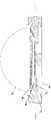
参考图2,本实用新型的多层式阵列型发光二极管光引擎的结构改良的第一实施例示意图。本实用新型是有关一种多层式阵列型发光二极管光引擎的结构改良,其可完全杜绝外界的湿气进入多层式阵列型发光二极管光引擎的封装结构的内部,防止内部的各光学组件因受潮而劣化。Referring to FIG. 2 , it is a schematic diagram of the first embodiment of the structural improvement of the multi-layer array LED light engine of the present invention. The utility model relates to a structural improvement of a multi-layer array type light-emitting diode light engine, which can completely prevent external moisture from entering the packaging structure of the multi-layer array type light-emitting diode light engine, preventing internal optical components from Deteriorated by moisture.
多层式阵列型发光二极管光引擎的封装结构至少包含有一基板1、一封装体3、两导线架对5。基板1可区分为中心区11及周边区13,中心区11的顶面为出光面111,中心区11涵盖于基板1的中心区块,较佳地中心区11的涵盖面积大于周边区13的涵盖面积,而周边区13为在中心区11及基板1边缘之间的区块,另周边区13具有顶面131、侧面133及底面135。The packaging structure of the multilayer array type LED light engine at least includes a
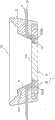
参考图3A,本实用新型的多层式阵列型发光二极管光引擎的结构改良的俯视示意图,参考图3B,图3B为图3A的区域A的局部剖视放大图,并配合图1所示。在顶面131上形成有两容置槽131A及131B及多个第一凹点1315,较佳地两容置槽131A及131B分别设置在顶面131上的相互对应的位置,较佳地两容置槽131A及131B可设置在尽量靠近于出光面111的位置,亦即让两容置槽131A及131B位于靠近出光面111的两侧,所述第一凹点1315可设置成环状,且所述第一凹点1315也可设置于两容置槽131A及131B之中。其中该中心区11的形状可以圆形、椭圆形、四边形、多边形及其它适当形状。Referring to FIG. 3A , it is a schematic top view of the improved structure of the multi-layer array LED light engine of the present invention. Referring to FIG. 3B , FIG. 3B is an enlarged partial cross-sectional view of area A in FIG. 3A , which is also shown in FIG. 1 . Two
封装体3包覆住基板1的周边区13的部分,但不包覆住中心区11,封装体3的包覆区域需涵盖顶面131、侧面133及底面135,其中封装体3具有封装腔室31,封装腔室31为封装体3未包覆住中心区11的部分,因此封装体3在中心区11的上方围构出容置空间,容置空间供封装腔室31之中可配置适当的光学构件,封装腔室31的底部恰为出光面111。The
封装腔室31的内壁面311与出光面111相互之间具有一夹角关系,较佳地夹角小于90度,当内壁面311与出光面111之间的夹角小于90度时,内壁面311面向于封装腔室31之外,因此当有光线射向到内壁面311时,将有助于光线被反射至封装腔室31之外,内壁面311之上可进一步设置光学反射罩4,透过在内壁面311之上设置光学反射罩4,更可大幅提升光线反射到封装腔室31之外的机率,使发光的照度得以提高。The
封装体3使用封装材料来包覆住基板1的周边区13的部分,其中封装材料可以是模塑树脂(Mold Resin),模塑树脂的材质可以是聚邻苯二甲酰胺压模树脂(poly-phthal-amide,PPA)或液晶聚合物(LiquidCrystalline Polymer,LCP)。The
参考图3A及图3B,并配合图2所示,两导线架5皆具有内端部51及外端部53,两导线架5的内端部51分别位于两容置槽131A及131B之中,其中外端部53的水平高度可高于内端部51的水平高度,如图1所示,两导线架5的其中一部分可形成有弯折段,弯折段的两端延伸出去即是两导线架5的内端部51及外端部53。Referring to FIG. 3A and FIG. 3B , and as shown in FIG. 2 , both lead
该两导线架5与该基板1之间相隔有该封装体3,且两导线架5的内端部51及外端部53之间的部分被封埋于封装体3之中,而内端部51及外端部53则露出于封装体3之外,其中该两导线架5的一面设置有多个第二凹点511,较佳地可将所述第二凹点设置在两导线架5的内端部51及在内端部51的周围区域。The
所述第一凹点1315及所述第二凹点511的设置分别在于增加封装体3对基板1及导线架5的接着性,因为导线架5使用具导电性质的金属制成,封装体3则使用塑料或树脂的材质,由于塑料或树脂不易与金属接合,但透过在导线架5设置有所述第二凹点511,可以增加导线架5的表面粗糙度,且所述第二凹点511还可以被液态的塑料或树脂填满,让液态的塑料或树脂可以布满导线架5的表面上,因此当液态的塑料或树脂固化后,可以增加封装体3对导线架5的接着性,使封装体3更加紧密地封合于导线架5。The setting of the first
参考图4,本实用新型的多层式阵列型发光二极管光引擎的结构改良的第二实施例示意图。其中在出光面111上可设置有多个发光二极管晶粒6,发光二极管晶粒6可以利用阵列性的排列方式配置在出光面111上,发光二极管晶粒6并与两导线架5构成电性连接,其中发光二极管晶粒6藉由打线接合与两导线架5而形成电性连接关系。Referring to FIG. 4 , it is a schematic diagram of a second embodiment of the improved structure of the multi-layer array LED light engine of the present invention. Wherein, a plurality of
其中所述发光二极管晶粒6藉由一焊膏(图未示)被焊设于该基板1的出光面111上,其中该焊膏可以是锡膏或银胶的至少其中之一,其中锡膏还可与碳晶与钻石晶体相混合,该钻石晶体还可镀上镍、银或其它导热性能优异的材质,透过在焊膏加入导热效果较佳的材料,可让焊膏的导热效能有效提升,藉以把发光二极管晶粒6所产生的热能快速地经由基板1传导至外部环境空间。Wherein the light-emitting
在所述发光二极管晶粒6之上可进一步形成有晶粒保护层7,晶粒保护层7须包覆所述发光二极管晶粒6,藉以保护所述发光二极管晶粒6免受外界的湿气及外界的污染,其中晶粒保护层7的材质为一硅胶,晶粒保护层7之上可再形成荧光胶层8,荧光胶层8可将所述发光二极管晶粒6所发出的光线予以混色。A grain protection layer 7 may be further formed on the
荧光胶层8之上更可形成硅胶隔离层9,硅胶隔离层9可隔绝外界的湿气侵入至荧光胶层8,如此荧光胶层8不会因受潮而变质。再者,在硅胶隔离层9之上可配置透镜10,且透镜10被底胶层20(underfilling)黏固于硅胶隔离层9之上,其中透镜10浮设于硅胶隔离层9之上,不与光学反射罩4直接接触,且硅胶隔离层9与透镜10都属于塑料材质,透镜10可紧密地固定于硅胶隔离层9之上,再者透过透镜10还可被底胶层20固定住,更可有效防止透镜10发生松动的情形,其中底胶层20的材质可以是环氧树脂或其它适当材质。A silica gel isolation layer 9 can be formed on the fluorescent adhesive layer 8, and the silica gel isolation layer 9 can isolate outside moisture from invading the fluorescent adhesive layer 8, so that the fluorescent adhesive layer 8 will not deteriorate due to moisture. Furthermore, the
其中硅胶隔离层9及透镜10之间可涂布有结合剂30(primer),结合剂30用增加硅胶隔离层9及透镜10之间的封密性,并阻绝外界湿气侵入于透镜10之内及硅胶隔离层9之下的荧光胶层8。A bonding agent 30 (primer) can be coated between the silica gel isolation layer 9 and the
参考图5,本实用新型的基板的第一实施例示意图,参考图6,本实用新型的基板的第二实施例示意图。其中基板1的顶面131上可形成有第一上沟槽1311,如图5所示。或者,也可如图6所示,在顶面131上进一步形成上凸部1313,其中在顶面131上可单独地设置第一上沟槽1311或上凸部1313,也可在顶面131上同时设置第一上沟槽1311及上凸部1313。Referring to FIG. 5 , a schematic diagram of the first embodiment of the substrate of the present invention, and referring to FIG. 6 , a schematic diagram of the second embodiment of the substrate of the present invention. A first
第一上沟槽1311的形状可以是U型、凹型、V型或其它适当的形状。要注意的是,上述第一上沟槽1311的数目与上凸部1313的数目视实际需要而定,在此仅是说明用的实例而已,并非用以限制本实用新型的范围。The shape of the first
参考图7,本实用新型的基板的第三实施例示意图。承上所述,在顶面上111可再设置出第二上沟槽1315,第二上沟槽1315设置在上凸部1313与基板1的边缘之间,第二上沟槽1315的形状可以是U型、凹型、V型或其它适当的形状。Referring to FIG. 7 , it is a schematic diagram of a third embodiment of the substrate of the present invention. Based on the above, a second
参考图8,本实用新型的基板的第四实施例示意图。在侧面133上可形成有侧沟槽1331,如图8所示。或者,也可如图9所示,在侧面133上设置出侧凸部1333,且侧凸部1333与在侧凸部1333之下的侧面133部分形成L型的结构,其中在侧面133上可单独地设置侧沟槽1331或侧凸部1333,也可在顶面133上同时设置侧沟槽1331及侧凸部1333。侧沟槽1331的形状可以是U型、凹型、V型或其它适当的形状。Referring to FIG. 8 , it is a schematic diagram of a fourth embodiment of the substrate of the present invention. A
参考图10,本实用新型的基板的第六实施例示意图。在底面135上可形成有下沟槽1351,如图10所示。或者,也可在底面135设置出一下凸部(图未示),其中在底面135上可单独地设置下沟槽1351或下凸部,也可在底面135上同时设置下沟槽1351及下凸部。Referring to FIG. 10 , it is a schematic diagram of a sixth embodiment of the substrate of the present invention. A
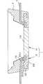
参考图11,本实用新型的多层式阵列型发光二极管光引擎的结构改良的一较佳实施例示意图。其中在本实用新型的较佳实施例中,可在透过周边区13的顶面131上由内至外依序设置两个第一上沟槽1311、一个上凸部1313及一个第二上沟槽1315,其中两个第一上沟槽1311皆设置成凹型状,第二上沟槽1315设置成V形状,而侧面133上形成侧凸部1333,且侧凸部1333与侧面133形成L型的结构,底面135则形成一个下沟槽1351。Referring to FIG. 11 , it is a schematic diagram of a preferred embodiment of the structural improvement of the multi-layer array LED light engine of the present invention. In a preferred embodiment of the present utility model, two first
参考图12A,图12A为图11的区域A的局部放大图,参考图12B,图12B为图11的区域B的局部放大图。其中两个第一上沟槽1311的内壁面上还可形成凸缘1311a,而在第二上沟槽1315的内壁面进一步形成凹缘1315a。Referring to FIG. 12A , FIG. 12A is a partially enlarged view of area A in FIG. 11 , and referring to FIG. 12B , which is a partially enlarged view of area B in FIG. 11 . The inner walls of the two first
上述的所述沟槽与所述沟槽可使液态状的封装材料可填流于所述沟槽之中,因此当封装材料形成固态状后,填流于所述沟槽的部分以及封装材料固态后所形成的封装体3的对应于凸部的部分会与基板1形成卡合的关系,如此基板1与封装体3会紧密地结合并固定成一体,不会因松脱而滑动,如此可增加基板与封装体的结构强度及封装密合度。The above-mentioned groove and the groove can make the liquid packaging material flow in the groove, so when the packaging material is in a solid state, the part filled in the groove and the packaging material The portion of the
尤其是当所述沟槽的内壁面上形成有凸缘1311a及凹缘1315a的时候,当封装材料形成固态状后,会分别与所述沟槽内壁面的凸缘1311a及凹缘1315a相卡合,使基板1可与封装体3更紧密地结合并固定成一体,使基板对封装体的结构强度及封装密合度更为强化。Especially when the flange 1311a and the
要注意的是,凸缘1311a及凹缘1315a的实际设置位置视实际需要而定,在此仅是说明用的实例而已,并非用以限制本实用新型的范围,亦即上述的任一沟槽及任一凸部都能视实际需要进一步设置凸缘1311a或凹缘1315a的至少其中之一,以提升本实用新型的封装结构的结构强度及封装密合度。It should be noted that the actual installation positions of the flange 1311a and the
以上所述仅为用以解释本实用新型的较佳实施例,并非企图据以对本实用新型做任何形式上的限制,因此,凡有在相同的发明精神下所作有关本实用新型的任何修饰或变更,皆仍应包括在本实用新型意图保护的范畴。The above descriptions are only preferred embodiments for explaining the utility model, and are not intended to limit the utility model in any form. Therefore, any modification or modification of the utility model made under the same spirit of the invention Changes should still be included in the scope of protection intended by the utility model.
Claims (38)
Translated fromChinesePriority Applications (1)
| Application Number | Priority Date | Filing Date | Title |
|---|---|---|---|
| CN2011203081318UCN202308030U (en) | 2011-08-23 | 2011-08-23 | Structure improvement of multi-layer array type LED light engine |
Applications Claiming Priority (1)
| Application Number | Priority Date | Filing Date | Title |
|---|---|---|---|
| CN2011203081318UCN202308030U (en) | 2011-08-23 | 2011-08-23 | Structure improvement of multi-layer array type LED light engine |
Publications (1)
| Publication Number | Publication Date |
|---|---|
| CN202308030Utrue CN202308030U (en) | 2012-07-04 |
Family
ID=46376864
Family Applications (1)
| Application Number | Title | Priority Date | Filing Date |
|---|---|---|---|
| CN2011203081318UExpired - Fee RelatedCN202308030U (en) | 2011-08-23 | 2011-08-23 | Structure improvement of multi-layer array type LED light engine |
Country Status (1)
| Country | Link |
|---|---|
| CN (1) | CN202308030U (en) |
Cited By (6)
| Publication number | Priority date | Publication date | Assignee | Title |
|---|---|---|---|---|
| CN107002986A (en)* | 2014-12-19 | 2017-08-01 | 通用电气照明解决方案有限责任公司 | Optical module assembly with reduced moisture ingress and method of manufacturing the same |
| CN107565003A (en)* | 2017-07-31 | 2018-01-09 | 深圳市华星光电技术有限公司 | Quantum dot LED encapsulation structure |
| CN108011016A (en)* | 2017-11-28 | 2018-05-08 | 西安科锐盛创新科技有限公司 | A kind of LED encapsulation structure |
| CN108011024A (en)* | 2017-11-28 | 2018-05-08 | 西安科锐盛创新科技有限公司 | LED light and LED packaging technologies |
| CN109003953A (en)* | 2018-08-08 | 2018-12-14 | 中山大学 | A kind of cooling fin |
| TWI708908B (en)* | 2019-06-10 | 2020-11-01 | 聯嘉光電股份有限公司 | Slim linear led lighting device |
- 2011
- 2011-08-23CNCN2011203081318Upatent/CN202308030U/ennot_activeExpired - Fee Related
Cited By (7)
| Publication number | Priority date | Publication date | Assignee | Title |
|---|---|---|---|---|
| CN107002986A (en)* | 2014-12-19 | 2017-08-01 | 通用电气照明解决方案有限责任公司 | Optical module assembly with reduced moisture ingress and method of manufacturing the same |
| CN107565003A (en)* | 2017-07-31 | 2018-01-09 | 深圳市华星光电技术有限公司 | Quantum dot LED encapsulation structure |
| CN107565003B (en)* | 2017-07-31 | 2019-04-30 | 深圳市华星光电技术有限公司 | Quantum dot LED encapsulation structure |
| CN108011016A (en)* | 2017-11-28 | 2018-05-08 | 西安科锐盛创新科技有限公司 | A kind of LED encapsulation structure |
| CN108011024A (en)* | 2017-11-28 | 2018-05-08 | 西安科锐盛创新科技有限公司 | LED light and LED packaging technologies |
| CN109003953A (en)* | 2018-08-08 | 2018-12-14 | 中山大学 | A kind of cooling fin |
| TWI708908B (en)* | 2019-06-10 | 2020-11-01 | 聯嘉光電股份有限公司 | Slim linear led lighting device |
Similar Documents
| Publication | Publication Date | Title |
|---|---|---|
| US8564005B2 (en) | Light-emitting device package | |
| CN202308030U (en) | Structure improvement of multi-layer array type LED light engine | |
| US8575645B2 (en) | Thin multi-layer LED array engine | |
| TWI463703B (en) | Light source device | |
| CN102956764B (en) | Packaging method of airtight multi-layer array type light-emitting diode | |
| CN104282831B (en) | A kind of LED encapsulation structure and packaging technology | |
| JP2016086168A (en) | Light-emitting apparatus and manufacturing method thereof | |
| JP2015015404A (en) | Led module and illumination device including the same | |
| CN102956789B (en) | Packaging structure of multi-layer array light-emitting diode light engine | |
| CN102306699A (en) | Integrated light-emitting diode (LED) packaging structure | |
| TWI513066B (en) | Light emitting diode package structure | |
| CN202585408U (en) | Structural Improvement of Multilayer Array Type Light-Emitting Diode Light Engine | |
| KR101401919B1 (en) | Lighting device of multi level type for integrated high-efficiency | |
| CN103208488A (en) | Thin multi-layer array type LED light engine | |
| US8338923B1 (en) | Package structure of multi-layer array type LED device | |
| JP3180453U7 (en) | ||
| JP3180453U (en) | Integrated high-efficiency lighting device with multilayer structure | |
| CN104319337A (en) | Substrate-free LED device and manufacturing method thereof | |
| TW201308677A (en) | Packaging structure of multi-layer array-type LED light engine | |
| CN102214645B (en) | Multi-layer Array Type Light Emitting Diodes | |
| CN202111091U (en) | Led integrated package structure | |
| TW201403870A (en) | Light emitting diode element and manufacturing mathod thereof | |
| CN202189782U (en) | Integrated encapsulating structure for COBLED (chip on board light-emitting diode) | |
| TWI479701B (en) | Light-emitting diode | |
| KR100621743B1 (en) | LED package with heat dissipation body |
Legal Events
| Date | Code | Title | Description |
|---|---|---|---|
| C14 | Grant of patent or utility model | ||
| GR01 | Patent grant | ||
| ASS | Succession or assignment of patent right | Owner name:YINGSHENG PHOTOELECTRIC TECHNOLOGY (SHANGHAI) CO., Free format text:FORMER OWNER: YINGSHENG TECHNOLOGY CO.,LTD. Effective date:20141223 | |
| C41 | Transfer of patent application or patent right or utility model | ||
| COR | Change of bibliographic data | Free format text:CORRECT: ADDRESS; FROM: TAIWAN, CHINA TO: 200438 YANGPU, SHANGHAI | |
| TR01 | Transfer of patent right | Effective date of registration:20141223 Address after:200438 Shanghai city Yangpu District Hengren Road No. 350 Building 1 room 110-4 Patentee after:Ying Guang photoelectric technology (Shanghai) Co., Ltd. Address before:Hsinchu County, Taiwan, China Patentee before:Ying Sheng Technology Co., Ltd. | |
| CF01 | Termination of patent right due to non-payment of annual fee | ||
| CF01 | Termination of patent right due to non-payment of annual fee | Granted publication date:20120704 Termination date:20180823 |