CN202178712U - Double-synchronous resonance switching type direct-current power supply - Google Patents
Double-synchronous resonance switching type direct-current power supplyDownload PDFInfo
- Publication number
- CN202178712U CN202178712UCN201120306081XUCN201120306081UCN202178712UCN 202178712 UCN202178712 UCN 202178712UCN 201120306081X UCN201120306081X UCN 201120306081XUCN 201120306081 UCN201120306081 UCN 201120306081UCN 202178712 UCN202178712 UCN 202178712U
- Authority
- CN
- China
- Prior art keywords
- circuit
- resonant
- electrically connected
- power supply
- power
- Prior art date
- Legal status (The legal status is an assumption and is not a legal conclusion. Google has not performed a legal analysis and makes no representation as to the accuracy of the status listed.)
- Expired - Fee Related
Links
- 238000006243chemical reactionMethods0.000claimsabstractdescription25
- 230000001360synchronised effectEffects0.000claimsabstractdescription25
- 230000009977dual effectEffects0.000claimsabstractdescription9
- 230000002159abnormal effectEffects0.000claimsdescription10
- 238000001514detection methodMethods0.000claimsdescription8
- 230000003287optical effectEffects0.000claimsdescription6
- 230000008878couplingEffects0.000claimsdescription4
- 238000010168coupling processMethods0.000claimsdescription4
- 238000005859coupling reactionMethods0.000claimsdescription4
- 238000001914filtrationMethods0.000claimsdescription4
- 230000000694effectsEffects0.000abstractdescription4
- 238000010586diagramMethods0.000description7
- 238000004146energy storageMethods0.000description6
- 238000004804windingMethods0.000description5
- 239000002184metalSubstances0.000description2
- 230000005855radiationEffects0.000description2
- 230000009286beneficial effectEffects0.000description1
- 239000013078crystalSubstances0.000description1
- 230000005611electricityEffects0.000description1
- 230000001939inductive effectEffects0.000description1
- 238000000034methodMethods0.000description1
- 230000010355oscillationEffects0.000description1
- 230000003071parasitic effectEffects0.000description1
- 238000007493shaping processMethods0.000description1
- 230000009466transformationEffects0.000description1
- 230000001960triggered effectEffects0.000description1
Images


Classifications
- H—ELECTRICITY
- H02—GENERATION; CONVERSION OR DISTRIBUTION OF ELECTRIC POWER
- H02M—APPARATUS FOR CONVERSION BETWEEN AC AND AC, BETWEEN AC AND DC, OR BETWEEN DC AND DC, AND FOR USE WITH MAINS OR SIMILAR POWER SUPPLY SYSTEMS; CONVERSION OF DC OR AC INPUT POWER INTO SURGE OUTPUT POWER; CONTROL OR REGULATION THEREOF
- H02M1/00—Details of apparatus for conversion
- H02M1/42—Circuits or arrangements for compensating for or adjusting power factor in converters or inverters
- H02M1/4208—Arrangements for improving power factor of AC input
- H02M1/4225—Arrangements for improving power factor of AC input using a non-isolated boost converter
- H—ELECTRICITY
- H02—GENERATION; CONVERSION OR DISTRIBUTION OF ELECTRIC POWER
- H02M—APPARATUS FOR CONVERSION BETWEEN AC AND AC, BETWEEN AC AND DC, OR BETWEEN DC AND DC, AND FOR USE WITH MAINS OR SIMILAR POWER SUPPLY SYSTEMS; CONVERSION OF DC OR AC INPUT POWER INTO SURGE OUTPUT POWER; CONTROL OR REGULATION THEREOF
- H02M3/00—Conversion of DC power input into DC power output
- H02M3/22—Conversion of DC power input into DC power output with intermediate conversion into AC
- H02M3/24—Conversion of DC power input into DC power output with intermediate conversion into AC by static converters
- H02M3/28—Conversion of DC power input into DC power output with intermediate conversion into AC by static converters using discharge tubes with control electrode or semiconductor devices with control electrode to produce the intermediate AC
- H02M3/325—Conversion of DC power input into DC power output with intermediate conversion into AC by static converters using discharge tubes with control electrode or semiconductor devices with control electrode to produce the intermediate AC using devices of a triode or a transistor type requiring continuous application of a control signal
- H02M3/335—Conversion of DC power input into DC power output with intermediate conversion into AC by static converters using discharge tubes with control electrode or semiconductor devices with control electrode to produce the intermediate AC using devices of a triode or a transistor type requiring continuous application of a control signal using semiconductor devices only
- H02M3/33569—Conversion of DC power input into DC power output with intermediate conversion into AC by static converters using discharge tubes with control electrode or semiconductor devices with control electrode to produce the intermediate AC using devices of a triode or a transistor type requiring continuous application of a control signal using semiconductor devices only having several active switching elements
- H02M3/33576—Conversion of DC power input into DC power output with intermediate conversion into AC by static converters using discharge tubes with control electrode or semiconductor devices with control electrode to produce the intermediate AC using devices of a triode or a transistor type requiring continuous application of a control signal using semiconductor devices only having several active switching elements having at least one active switching element at the secondary side of an isolation transformer
- H02M3/33592—Conversion of DC power input into DC power output with intermediate conversion into AC by static converters using discharge tubes with control electrode or semiconductor devices with control electrode to produce the intermediate AC using devices of a triode or a transistor type requiring continuous application of a control signal using semiconductor devices only having several active switching elements having at least one active switching element at the secondary side of an isolation transformer having a synchronous rectifier circuit or a synchronous freewheeling circuit at the secondary side of an isolation transformer
- H—ELECTRICITY
- H02—GENERATION; CONVERSION OR DISTRIBUTION OF ELECTRIC POWER
- H02M—APPARATUS FOR CONVERSION BETWEEN AC AND AC, BETWEEN AC AND DC, OR BETWEEN DC AND DC, AND FOR USE WITH MAINS OR SIMILAR POWER SUPPLY SYSTEMS; CONVERSION OF DC OR AC INPUT POWER INTO SURGE OUTPUT POWER; CONTROL OR REGULATION THEREOF
- H02M3/00—Conversion of DC power input into DC power output
- H02M3/22—Conversion of DC power input into DC power output with intermediate conversion into AC
- H02M3/24—Conversion of DC power input into DC power output with intermediate conversion into AC by static converters
- H02M3/28—Conversion of DC power input into DC power output with intermediate conversion into AC by static converters using discharge tubes with control electrode or semiconductor devices with control electrode to produce the intermediate AC
- H02M3/325—Conversion of DC power input into DC power output with intermediate conversion into AC by static converters using discharge tubes with control electrode or semiconductor devices with control electrode to produce the intermediate AC using devices of a triode or a transistor type requiring continuous application of a control signal
- H02M3/335—Conversion of DC power input into DC power output with intermediate conversion into AC by static converters using discharge tubes with control electrode or semiconductor devices with control electrode to produce the intermediate AC using devices of a triode or a transistor type requiring continuous application of a control signal using semiconductor devices only
- H02M3/338—Conversion of DC power input into DC power output with intermediate conversion into AC by static converters using discharge tubes with control electrode or semiconductor devices with control electrode to produce the intermediate AC using devices of a triode or a transistor type requiring continuous application of a control signal using semiconductor devices only in a self-oscillating arrangement
- H02M3/3385—Conversion of DC power input into DC power output with intermediate conversion into AC by static converters using discharge tubes with control electrode or semiconductor devices with control electrode to produce the intermediate AC using devices of a triode or a transistor type requiring continuous application of a control signal using semiconductor devices only in a self-oscillating arrangement with automatic control of output voltage or current
- H02M3/3387—Conversion of DC power input into DC power output with intermediate conversion into AC by static converters using discharge tubes with control electrode or semiconductor devices with control electrode to produce the intermediate AC using devices of a triode or a transistor type requiring continuous application of a control signal using semiconductor devices only in a self-oscillating arrangement with automatic control of output voltage or current in a push-pull configuration
- Y—GENERAL TAGGING OF NEW TECHNOLOGICAL DEVELOPMENTS; GENERAL TAGGING OF CROSS-SECTIONAL TECHNOLOGIES SPANNING OVER SEVERAL SECTIONS OF THE IPC; TECHNICAL SUBJECTS COVERED BY FORMER USPC CROSS-REFERENCE ART COLLECTIONS [XRACs] AND DIGESTS
- Y02—TECHNOLOGIES OR APPLICATIONS FOR MITIGATION OR ADAPTATION AGAINST CLIMATE CHANGE
- Y02B—CLIMATE CHANGE MITIGATION TECHNOLOGIES RELATED TO BUILDINGS, e.g. HOUSING, HOUSE APPLIANCES OR RELATED END-USER APPLICATIONS
- Y02B70/00—Technologies for an efficient end-user side electric power management and consumption
- Y02B70/10—Technologies improving the efficiency by using switched-mode power supplies [SMPS], i.e. efficient power electronics conversion e.g. power factor correction or reduction of losses in power supplies or efficient standby modes
- Y—GENERAL TAGGING OF NEW TECHNOLOGICAL DEVELOPMENTS; GENERAL TAGGING OF CROSS-SECTIONAL TECHNOLOGIES SPANNING OVER SEVERAL SECTIONS OF THE IPC; TECHNICAL SUBJECTS COVERED BY FORMER USPC CROSS-REFERENCE ART COLLECTIONS [XRACs] AND DIGESTS
- Y02—TECHNOLOGIES OR APPLICATIONS FOR MITIGATION OR ADAPTATION AGAINST CLIMATE CHANGE
- Y02P—CLIMATE CHANGE MITIGATION TECHNOLOGIES IN THE PRODUCTION OR PROCESSING OF GOODS
- Y02P80/00—Climate change mitigation technologies for sector-wide applications
- Y02P80/10—Efficient use of energy, e.g. using compressed air or pressurized fluid as energy carrier
Landscapes
- Engineering & Computer Science (AREA)
- Power Engineering (AREA)
- Dc-Dc Converters (AREA)
Abstract
Translated fromChinese
Description
Translated fromChinese技术领域technical field
本实用新型涉及一种切换式直流电源供应器,特别是涉及一种双同步谐振切换式直流电源供应器。The utility model relates to a switchable DC power supply, in particular to a double synchronous resonance switchable DC power supply.
背景技术Background technique
电源转换器是所有电子产品或设备运作所必须的动力来源,在亟需节约能源潮流的驱使下,电源转换器往往需要达到省能环保的设计。Power converters are the necessary source of power for the operation of all electronic products or equipment. Driven by the urgent need to save energy, power converters often need to achieve energy-saving and environmentally friendly designs.
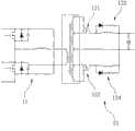
参阅图1,为中国台湾公告第I309914号「半桥共振转换器」,包含一个一次侧绕组11,及一个二次侧绕组12,该二次侧绕组12具有一第一电子开关121、一第二电子开关122、一第一储能组件123,及一第二储能组件124。该第一电子开关121是由一MOSFET功率电晶体与一绕组结合,该第二电子开关122是由另一MOSFET功率电晶体与另一绕组结合,该第一储能组件123是由一滤波电感并联二极管与电阻串联的组合,该第二储能组件124是由另一滤波电感并联二极管与电阻串联的组合;借由上述第一电子开关121、第二电子开关122的设计能够达到同步整流的目的,同时利用该第一储能组件123、第二储能组件124可避免第一电子开关121、第二电子开关122因逆向偏压所造成的能量损耗。Referring to Fig. 1, it is "half bridge resonant converter" No. I309914 of China Taiwan Announcement, comprises a primary side winding 11, and a secondary side winding 12, and this secondary side winding 12 has a first
不过,由于该半桥共振转换器往往会因为输出讯号的功率损耗或负载的电感性、电容性等影响,使输出讯号的电压与电流的相位差过大,而造成功率因数下降的问题,因此,如何能够提高功率因数便成为相关业者亟欲努力的目标。However, due to the power loss of the output signal or the inductive and capacitive effects of the load in the half-bridge resonant converter, the phase difference between the voltage and current of the output signal is too large, resulting in a problem of power factor drop. Therefore, how to improve the power factor has become an urgent goal for relevant industry players.
发明内容Contents of the invention
本实用新型的目的在于提供一种可提高功率因数及使用效率的双同步谐振切换式直流电源供应器。The purpose of the utility model is to provide a dual-synchronous resonant switching DC power supply that can improve power factor and use efficiency.
本实用新型双同步谐振切换式直流电源供应器,包含一个电源供应单元、一个功因修正单元、一个谐振式转换单元,及一个同步整流单元。The utility model dual-synchronous resonant switchable DC power supply comprises a power supply unit, a power factor correction unit, a resonant conversion unit, and a synchronous rectification unit.
该电源供应单元包括一个能够源引一交流电源的电源供应电路,及一个电连接该电源供应电路且可将该交流电源整流滤波成一直流电压输出的整流滤波电路。The power supply unit includes a power supply circuit that can source an AC power supply, and a rectification filter circuit that is electrically connected to the power supply circuit and can rectify and filter the AC power supply into a DC voltage output.
该功因修正单元包括一个电连接该整流滤波电路的升压电路、一个电连接该升压电路的主动式功因修正晶片电路,及两个并联且电连接该主动式功因修正晶片电路的电晶体控制电路。The power factor correction unit includes a boost circuit electrically connected to the rectification filter circuit, an active power factor correction chip circuit electrically connected to the boost circuit, and two parallel and electrically connected to the active power factor correction chip circuit Transistor control circuit.
该谐振式转换单元包括一个电连接该升压电路的功率开关电路、一个电连接该功率开关电路而能交互切换该功率开关电路导通的谐振晶片电路,以及一个电连接该功率开关电路的电压转换电路,该电压转换电路具有一个与该功率开关电路电连接的第一次侧端线圈,以及一个耦接该第一次侧端线圈的第二次侧端线圈。The resonant conversion unit includes a power switch circuit electrically connected to the boost circuit, a resonant chip circuit electrically connected to the power switch circuit and capable of alternately switching the conduction of the power switch circuit, and a voltage circuit electrically connected to the power switch circuit A conversion circuit, the voltage conversion circuit has a first side coil electrically connected to the power switch circuit, and a second side coil coupled to the first side coil.
该同步整流单元包括分别电连接该谐振式转换单元的第二次侧端线圈两端的一个第一谐振桥式整流电路与一个第二谐振桥式整流电路,及一个电连接该第一谐振桥式整流电路、第二谐振桥式整流电路的供电电压输出电路。The synchronous rectification unit includes a first resonant bridge rectifier circuit and a second resonant bridge rectifier circuit electrically connected to both ends of the second secondary side coil of the resonant conversion unit, and a resonant bridge rectifier circuit electrically connected to the first resonant bridge The rectifier circuit and the power supply voltage output circuit of the second resonant bridge rectifier circuit.
本实用新型的目的及解决其技术问题还可采用以下技术措施进一步实现。The purpose of the utility model and the solution to its technical problems can also be further realized by adopting the following technical measures.
较佳地,前述的双同步谐振切换式直流电源供应器,还包含一个电连接该供电电压输出电路的异常电压电流侦测单元,该异常电压电流侦测单元包括一个定电压定电流放大电路、一个电连接该定电压定电流放大电路的输出电压调整电路、分别与该定电压定电流放大电路电连接的一个第一光耦合器及一个第二光耦合器,该谐振式转换单元的谐振晶片电路具有一个能与该第一光耦合器进行光耦合的第一耦接器,该功因修正单元的主动式功因修正晶片电路具有一个能与该第二光耦合器进行光耦合的第二耦接器。Preferably, the aforementioned dual synchronous resonant switching DC power supply also includes an abnormal voltage and current detection unit electrically connected to the supply voltage output circuit, and the abnormal voltage and current detection unit includes a constant voltage and constant current amplifier circuit, An output voltage adjustment circuit electrically connected to the constant voltage and constant current amplifying circuit, a first optocoupler and a second optocoupler electrically connected to the constant voltage and constant current amplifying circuit respectively, the resonant chip of the resonant conversion unit The circuit has a first coupler that can be optically coupled with the first optical coupler, and the active power factor correction chip circuit of the power factor correction unit has a second coupler that can be optically coupled with the second optical coupler. coupler.
较佳地,前述的双同步谐振切换式直流电源供应器,其中该电源供应单元还包括一个电连接在该电源供应电路与该整流滤波电路间的抗扰电路。Preferably, in the aforementioned dual synchronous resonant switching DC power supply, the power supply unit further includes an anti-interference circuit electrically connected between the power supply circuit and the rectification and filtering circuit.
本实用新型的有益效果在于:借由该功因修正单元是使用两个并联设置并同时受主动式功因修正晶片电路控制导通及截止的电晶体,而能更有效地提高功率因数以降低虚功的消耗,同时借由该同步整流单元是使用该第一谐振桥式整流电路与该第二谐振桥式整流电路,来分别对该谐振式转换单元的第二次端侧线圈所转换输出之正、负半周的交流电压进行双同步的整流,而能有效提高该切换式直流电源供应器的使用效率,进而达到节能省电的效果。The beneficial effect of the utility model is that: the power factor correction unit uses two transistors connected in parallel and controlled by the active power factor correction chip circuit to turn on and off at the same time, so that the power factor can be improved more effectively to reduce the consumption of reactive power, and at the same time, the synchronous rectification unit uses the first resonant bridge rectifier circuit and the second resonant bridge rectifier circuit to convert the output of the second end-side coil of the resonant conversion unit respectively The positive and negative half-cycle AC voltages are double-synchronously rectified, which can effectively improve the efficiency of the switching DC power supply, thereby achieving the effect of energy saving.
附图说明Description of drawings
图1是一电路图,说明中国台湾公告第I309914号「半桥共振转换器」发明专利案的电路结构;FIG. 1 is a circuit diagram illustrating the circuit structure of the invention patent case of "half-bridge resonant converter" in Taiwan Announcement No. I309914;
图2是一功能方块图,说明本实用新型双同步谐振切换式直流电源供应器的较佳实施例的整体架构;Fig. 2 is a functional block diagram illustrating the overall architecture of a preferred embodiment of the dual synchronous resonant switching DC power supply of the present invention;
图3是一电路图,说明该较佳实施例的电源供应单元;Fig. 3 is a circuit diagram illustrating the power supply unit of the preferred embodiment;
图4是一电路图,说明该较佳实施例的功因修正单元;Fig. 4 is a circuit diagram illustrating the power factor correction unit of the preferred embodiment;
图5是一电路图,说明该较佳实施例的谐振式转换单元;FIG. 5 is a circuit diagram illustrating the resonant conversion unit of the preferred embodiment;
图6是一电路图,说明该较佳实施例的同步整流单元;Fig. 6 is a circuit diagram illustrating the synchronous rectification unit of the preferred embodiment;
图7是一电路图,说明该较佳实施例的异常电压电流侦测单元。FIG. 7 is a circuit diagram illustrating the abnormal voltage and current detection unit of the preferred embodiment.
具体实施方式Detailed ways
下面结合附图及实施例对本实用新型进行详细说明。Below in conjunction with accompanying drawing and embodiment the utility model is described in detail.
参阅图2,本实用新型双同步谐振切换式直流电源供应器的较佳实施例,包含一电源供应单元2、一功因修正单元3、一谐振式转换单元4、一同步整流单元5,及一异常电压电流侦测单元6。Referring to Fig. 2, a preferred embodiment of the dual synchronous resonant switching DC power supply of the present invention includes a
参阅图2、3,该电源供应单元2包括一可源引一交流电源Vac的电源供应电路21、一电连接该电源供应电路21且可将该交流电源Vac整流滤波成一直流电压Va输出的整流滤波电路23,及一电连接在该电源供应电路21与该整流滤波电路23间的抗扰电路22,该抗扰电路22为EMC(Electromagnetic Compatibility)电路,借以防止电磁干扰、辐射干扰或导线传导干扰而影响到电路的性能。2 and 3, the
参阅图2、3、4,该功因修正单元3包括一电连接该整流滤波电路23的升压电路31、一电连接该升压电路31的主动式功因修正晶片电路32,及两个并联且电连接该主动式功因修正晶片电路32的电晶体控制电路33、34,该主动式功因修正晶片电路32可同时触发导通及截止该两电晶体控制电路33、34。2, 3, 4, the power
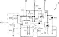
参阅图2、4、5,该谐振式转换单元4包括一电连接该升压电路31的功率开关电路41、一电连接该功率开关电路41而能交互切换该功率开关电路41导通的谐振晶片电路42,以及一电连接该功率开关电路41的电压转换电路43,该电压转换电路43具有一与该功率开关电路41电连接的第一次侧端线圈T1,以及一耦接该第一次侧端线圈T 1的第二次侧端线圈T2,该第二次侧端线圈T2是采用中间抽头整流方式电连接后端的同步整流单元5(显示于图6)。2, 4, 5, the
参阅图2、5、6,该同步整流单元5包括分别电连接于该第二次侧端线圈T2两端的一第一谐振桥式整流电路51与一第二谐振桥式整流电路52,及一电连接该第一谐振桥式整流电路51、第二谐振桥式整流电路52的供电电压输出电路53。Referring to Figures 2, 5, and 6, the
参阅图2、6、7,该异常电压电流侦测单元6是与该供电电压输出电路53电连接,其包括一定电压定电流放大电路61、一电连接该定电压定电流放大电路61的输出电压调整电路62、与该定电压定电流放大电路61电连接的一第一光耦合器63及一第二光耦合器64;配合参阅图5,该谐振式转换单元4的谐振晶片电路42是电连接一能与该第一光耦合器63进行光耦合的第一耦接器PH1;配合参阅图4,该功因修正单元3的主动式功因修正晶片电路32是电连接一能与该第二光耦合器64进行光耦合的第二耦接器PH2。Referring to Figures 2, 6, and 7, the abnormal voltage and
请参阅图2、3、4,本实施例的切换式直流电源供应器于运作时,是借由该电源供应单元2的电源供应电路21将一般市电(70V~264V)的交流电源Vac源引进来,通过该抗扰电路22作防止电磁或幅射干扰后再经由该整流滤波电路23进行整流滤波而输出一直流电压Va,接着,该直流电压Va经该功因修正单元3的电阻R3、R4、R5、R6分压后输入该主动式功因修正晶片电路32的一功率因数(PFC)IC1,同时该直流电压Va另外经一个二极管D1再经电阻R8、R9、R10、R11、R12分压后,另输出一回授电压Vf而同样回授输入该PFC IC1,可使当远程负载改变时,经由该升压电路31所输出的高直流电压Vb仍能保持在固定的准位;再者,该二并联设置的晶体管控制电路33、34的源极端电压Vs是经由电阻R18回授输入该PFC IC1,使该PFC IC1就以该直流电压Va、该回授电压Vf的回授信号与该源极端电压Vs的回授信号来作比较并控制触发导通或截止该二并联设置的电晶体控制电路33、34中的MOSFET电晶体Q1、Q5的时间,借此达到将直流电压Va的电流波形整形以追上其电压相位的目的,以将其电压与电流的相位差缩小而相对修正提高其功率因数。Please refer to Fig. 2, 3, 4, when the switchable DC power supply of the present embodiment is in operation, the AC power Vac source of the general commercial power (70V ~ 264V) is supplied by the
本实施例的功率因数的均值可维持于90%以上;另外,由于本实施例是使用两个并联设置并同时受该主动式功因修正晶片电路32的PFC IC1控制导通及截止的电晶体Q1、Q5,搭配该升压电路31的电感器L3的作用,因此当该二电晶体Q1、Q5同时导通时,能大幅增加流经该电感器L3的电流,相对地,当该二电晶体Q1、Q5截止时,便能大幅缩短经由该电感器L3所放电升压输出的高直流电压Vb(大约是380V~400V)的时间。The average value of the power factor of the present embodiment can be maintained at more than 90%; in addition, because the present embodiment uses two transistors connected in parallel and simultaneously controlled by the PFC IC1 of the active power factor correction chip circuit 32 to turn on and off Q1, Q5, in conjunction with the role of the inductor L3 of the boost circuit 31, so when the two transistors Q1, Q5 are turned on at the same time, can greatly increase the current flowing through the inductor L3, relatively, when the two transistors When the crystals Q1 and Q5 are turned off, the time for the high DC voltage Vb (approximately 380V-400V) discharged and boosted by the inductor L3 can be greatly shortened.
参阅图2、4、5,该谐振式转换单元4主要是要将该功因修正单元3所输出的高直流电压Vb转换到负载所需的电压,其主要是利用该谐振晶片电路42的一LLC IC2与该功率开关电路41的MOSFET功率电晶体Q3、Q4的寄生电容C17产生共振,而振荡产生两个各50%工作周期且能交互触发切换导通该二功率电晶体Q3、Q4的谐振频率讯号,且该LLC IC2能使该二功率电晶体Q3、Q4在零电压切换损失的状态下,可视负载的轻重而改变触发导通该二功率电晶体Q3、Q4的讯号切换频率,借以将该功因修正单元3所输出的高直流电压Vb转换成一弦波的电压输出至该电压转换电路43的第一次侧端线圈T1,并与第二次侧端线圈T2耦合变压后,转换成一具有正、负弦波的交流电压输出。当负载属于轻载时,触发导通该二功率电晶体Q3、Q4的讯号切换频率是高于谐振频率,以使增益降低,当负载处于重载时,触发导通该二功率电晶体Q3、Q4的讯号切换频率是低于谐振频率,以使增益提高,而在一般状况的负载时,是将触发导通该二功率电晶体Q3、Q4的讯号切换频率操作于谐振频率附近,以维持适当增益。Referring to Figures 2, 4, and 5, the
参阅图2、5、6,该谐振式转换单元4所转换输出的正、负弦波的交流电压,借由该同步整流单元5将其中的正弦波及负弦波的部分分别经过该第一谐振桥式整流电路51与第二谐振桥式整流电路52,利用其中的同步整流IC4、IC5能够同时将该具有正、负弦波的交流电压进行双同步地整流及滤波成一直流电压,再经该供电电压输出电路53的稳压后,就能转换成一最终输出的稳定直流电源Vdc,而能有效提高本实施例的切换式直流电源供应器的使用效率。Referring to Figures 2, 5, and 6, the positive and negative sine wave AC voltages converted and output by the
参阅图2、6、7,利用该异常电压电流侦测单元6的定电压定电流放大电路61,能够使该供电电压输出电路53所输出的直流电源Vdc稳定地供应给负载,同时,借由该输出电压调整电路62的可变电阻VR1的适当调整,能够设定该供电电压输出电路53所欲输出的直流电源Vdc的电压;再者,利用该定电压定电流放大电路61的微阻值金属电阻RS1,能够精密地侦测该供电电压输出电路53所输出的直流电源Vdc端的负载变化,并适时回授给该定电压定电流放大电路61,若侦测到直流电源Vdc端的负载有异常电压时,该定电压定电流放大电路61就会驱动该第一光耦合器63动作,而与电连接于该谐振式转换单元4的谐振晶片电路42上的第一耦接器PH1进行光耦合,而关闭该谐振晶片电路42;若该微阻值金属电阻RS1侦测到直流电源Vdc端的负载有异常电流时,该定电压定电流放大电路61就会驱动该第二光耦合器64动作,而与电连接于该功因修正单元3的主动式功因修正晶片电路32上的第二耦接器PH2进行光耦合,而关闭该主动式功因修正晶片电路32,以达到对本实施例的切换式直流电源供应器的保护作用。Referring to Figures 2, 6, and 7, the constant voltage and constant current amplifying
本实用新型双同步谐振切换式直流电源供应器,借由该功因修正单元3是使用两个并联设置并同时受主动式功因修正晶片电路32控制导通及截止的电晶体Q1、Q5,而能更有效地提高功率因数以降低虚功的消耗,同时借由该同步整流单元5是使用该第一谐振桥式整流电路51与第二谐振桥式整流电路52,来分别对该谐振式转换单元4的第二次侧端线圈T2所转换输出的正、负弦波的交流电压进行双同步的整流及滤波,而能有效提高该切换式直流电源供应器的使用效率,进而达到节能省电的效果。The dual-synchronous resonant switching DC power supply of the present invention uses two transistors Q1 and Q5 which are connected in parallel and controlled by the active power factor correction chip circuit 32 to turn on and off, by means of the power
Claims (3)
Translated fromChineseApplications Claiming Priority (2)
| Application Number | Priority Date | Filing Date | Title |
|---|---|---|---|
| TW100212366 | 2011-07-06 | ||
| TW100212366UTWM417719U (en) | 2011-07-06 | 2011-07-06 | Bisynchronous Resonant Switching DC power supply |
Publications (1)
| Publication Number | Publication Date |
|---|---|
| CN202178712Utrue CN202178712U (en) | 2012-03-28 |
Family
ID=45868575
Family Applications (1)
| Application Number | Title | Priority Date | Filing Date |
|---|---|---|---|
| CN201120306081XUExpired - Fee RelatedCN202178712U (en) | 2011-07-06 | 2011-08-22 | Double-synchronous resonance switching type direct-current power supply |
Country Status (4)
| Country | Link |
|---|---|
| US (1) | US20130010501A1 (en) |
| JP (1) | JP3173908U (en) |
| CN (1) | CN202178712U (en) |
| TW (1) | TWM417719U (en) |
Cited By (4)
| Publication number | Priority date | Publication date | Assignee | Title |
|---|---|---|---|---|
| CN103144779A (en)* | 2012-11-30 | 2013-06-12 | 中国电子科技集团公司第七研究所 | Multi-rotor-wing unmanned aerial vehicle mooring system |
| TWI549410B (en)* | 2014-09-19 | 2016-09-11 | 茂力科技股份有限公司 | Switching mode power supply and the method thereof |
| CN106527648A (en)* | 2016-10-25 | 2017-03-22 | 郑州云海信息技术有限公司 | Power supply device and method of server |
| CN108988663A (en)* | 2018-06-11 | 2018-12-11 | 珠海格力智能装备有限公司 | Switching power supply circuit and switching power supply |
Families Citing this family (8)
| Publication number | Priority date | Publication date | Assignee | Title |
|---|---|---|---|---|
| TWI458146B (en)* | 2011-12-30 | 2014-10-21 | Champion Elite Co Ltd | Piezoelectric drive circuit with zero voltage switching |
| CN103151829B (en)* | 2013-03-12 | 2015-04-22 | 重庆九亿光电仪器有限公司 | Two-channel direct-current (DC) output waterproof constant current power supply |
| CN105322803B (en)* | 2015-11-02 | 2018-03-06 | 深圳创维-Rgb电子有限公司 | Constant pressure and flow synchronism output power supply and television set |
| TWI692190B (en)* | 2018-09-12 | 2020-04-21 | 邱煌仁 | Series resonant converter |
| EP3972105A1 (en)* | 2020-09-16 | 2022-03-23 | Infineon Technologies Austria AG | Power conversion method using a synergetic control of two power converters |
| CN112366963B (en)* | 2020-11-04 | 2025-04-01 | 江阴旺达电子有限公司 | A driving power supply circuit based on gallium nitride power chip |
| CN114975610A (en)* | 2021-02-25 | 2022-08-30 | 广东美的白色家电技术创新中心有限公司 | Semiconductor device assembly, integrated circuit and electric appliance |
| CN115113671B (en)* | 2021-03-23 | 2024-03-12 | 西安青松光电技术有限公司 | Power supply device and electronic equipment |
Family Cites Families (5)
| Publication number | Priority date | Publication date | Assignee | Title |
|---|---|---|---|---|
| US5359274A (en)* | 1992-08-20 | 1994-10-25 | North American Philips Corporation | Active offset for power factor controller |
| JP4193755B2 (en)* | 2004-06-04 | 2008-12-10 | サンケン電気株式会社 | Switching power supply device and power factor correction circuit |
| US7764516B2 (en)* | 2008-02-21 | 2010-07-27 | System General Corporation | Method and apparatus of providing synchronous regulation circuit for offline power converter |
| JP2011217427A (en)* | 2010-03-31 | 2011-10-27 | Renesas Electronics Corp | Electronic device and semiconductor device |
| US8953341B2 (en)* | 2011-05-09 | 2015-02-10 | Infineon Technologies Ag | Converter with reduced power consumption |
- 2011
- 2011-07-06TWTW100212366Upatent/TWM417719U/ennot_activeIP Right Cessation
- 2011-08-22CNCN201120306081XUpatent/CN202178712U/ennot_activeExpired - Fee Related
- 2011-10-28USUS13/284,651patent/US20130010501A1/ennot_activeAbandoned
- 2011-12-15JPJP2011007411Upatent/JP3173908U/ennot_activeExpired - Fee Related
Cited By (5)
| Publication number | Priority date | Publication date | Assignee | Title |
|---|---|---|---|---|
| CN103144779A (en)* | 2012-11-30 | 2013-06-12 | 中国电子科技集团公司第七研究所 | Multi-rotor-wing unmanned aerial vehicle mooring system |
| CN103144779B (en)* | 2012-11-30 | 2016-01-13 | 中国电子科技集团公司第七研究所 | Many rotor unmanned aircrafts mooring system |
| TWI549410B (en)* | 2014-09-19 | 2016-09-11 | 茂力科技股份有限公司 | Switching mode power supply and the method thereof |
| CN106527648A (en)* | 2016-10-25 | 2017-03-22 | 郑州云海信息技术有限公司 | Power supply device and method of server |
| CN108988663A (en)* | 2018-06-11 | 2018-12-11 | 珠海格力智能装备有限公司 | Switching power supply circuit and switching power supply |
Also Published As
| Publication number | Publication date |
|---|---|
| JP3173908U (en) | 2012-02-23 |
| US20130010501A1 (en) | 2013-01-10 |
| TWM417719U (en) | 2011-12-01 |
Similar Documents
| Publication | Publication Date | Title |
|---|---|---|
| CN202178712U (en) | Double-synchronous resonance switching type direct-current power supply | |
| CN101854120B (en) | A High Efficiency Multifunctional Flyback Converter | |
| Cho et al. | Single power-conversion AC--DC converter with high power factor and high efficiency | |
| CN101685980B (en) | Full-bridge zero-voltage boost switching resonant converter based on LLC used for UPS | |
| EP1816537A2 (en) | Switching power supply circuit | |
| CN103580468B (en) | Passive Power Factor Correction Circuit | |
| CN103973138B (en) | Dynamic variable frequency power conversion system | |
| CN103025009B (en) | A kind of LED Drive and Control Circuit | |
| CN201054545Y (en) | Middle power multi-channel output thin switch power supply | |
| CN106535402B (en) | A kind of LED drive circuit that single-stage single-switch buck leakage inductance energy utilizes | |
| TWI514733B (en) | Non-contact transformer system | |
| CN202455256U (en) | Speed adjustment controller of dual-purpose compressor with alternating current-direct current | |
| CN105792447B (en) | The LED drive circuit and its high power factor correction device of no electrolytic capacitor | |
| CN201113883Y (en) | Portable type generator set inversion type control device | |
| CN201199672Y (en) | Flyback converter with single-stage power factor correction circuit | |
| CN203482094U (en) | Efficient power conversion device | |
| TW201433058A (en) | Dynamic variable-frequency power conversion system | |
| CN211240163U (en) | Stage lamp photoelectronic ballast | |
| EP2544348A2 (en) | Bisynchronous resonant switching-type direct current power supply | |
| CN1286523A (en) | Sigle-stage AC/DC converter with power factor correction | |
| CN217824731U (en) | A single-stage LLC switching power supply circuit | |
| TW201820758A (en) | Single-phase bridgeless isolating power factor adjusting circuit capable of achieving low conduction loss, not easy for breakdown, simple circuit, cost saving, small volume and high conversion efficiency | |
| CA2965014C (en) | Isolated step-up converter | |
| CN201839206U (en) | Improved alternating current and direct current switching power supply circuit structure | |
| Huang et al. | Analysis and design of a single-stage buck-type AC-DC adaptor |
Legal Events
| Date | Code | Title | Description |
|---|---|---|---|
| C14 | Grant of patent or utility model | ||
| GR01 | Patent grant | ||
| ASS | Succession or assignment of patent right | Owner name:DELIN INTERNATIONAL ENERGY CO., LTD. Free format text:FORMER OWNER: HUANG WENJIN Effective date:20120222 | |
| C41 | Transfer of patent application or patent right or utility model | ||
| TR01 | Transfer of patent right | Effective date of registration:20120222 Address after:Kaohsiung City, Taiwan, China Patentee after:Tak Lin International Energy Limited by Share Ltd Address before:Kaohsiung City, Taiwan, China Patentee before:Huang Wenjin | |
| ASS | Succession or assignment of patent right | Owner name:FUDING ENERGY TECHNOLOGY CO., LTD. Free format text:FORMER OWNER: DELIN INTERNATIONAL ENERGY CO., LTD. Effective date:20120828 | |
| C41 | Transfer of patent application or patent right or utility model | ||
| TR01 | Transfer of patent right | Effective date of registration:20120828 Address after:Kaohsiung City, Taiwan, China Patentee after:Fu Ting Energy Technology Co Ltd Address before:Kaohsiung City, Taiwan, China Patentee before:Tak Lin International Energy Limited by Share Ltd | |
| CF01 | Termination of patent right due to non-payment of annual fee | Granted publication date:20120328 Termination date:20140822 | |
| EXPY | Termination of patent right or utility model |