CN202053682U - Recording material supply system, circuit board, construction body and cartridge - Google Patents
Recording material supply system, circuit board, construction body and cartridgeDownload PDFInfo
- Publication number
- CN202053682U CN202053682UCN2010201988260UCN201020198826UCN202053682UCN 202053682 UCN202053682 UCN 202053682UCN 2010201988260 UCN2010201988260 UCN 2010201988260UCN 201020198826 UCN201020198826 UCN 201020198826UCN 202053682 UCN202053682 UCN 202053682U
- Authority
- CN
- China
- Prior art keywords
- terminals
- recording material
- receiving
- terminal
- ink
- Prior art date
- Legal status (The legal status is an assumption and is not a legal conclusion. Google has not performed a legal analysis and makes no representation as to the accuracy of the status listed.)
- Expired - Fee Related
Links
- 239000000463materialSubstances0.000titleclaimsabstractdescription116
- 238000010276constructionMethods0.000title1
- 239000000758substrateSubstances0.000claimsabstractdescription76
- 238000009434installationMethods0.000claimsdescription17
- 230000005484gravityEffects0.000claimsdescription4
- 238000001514detection methodMethods0.000abstractdescription31
- 239000000976inkSubstances0.000description429
- 230000015654memoryEffects0.000description82
- 230000007246mechanismEffects0.000description38
- 238000010586diagramMethods0.000description35
- 238000000034methodMethods0.000description25
- 238000012545processingMethods0.000description22
- 230000008901benefitEffects0.000description14
- 230000008569processEffects0.000description10
- 230000004044responseEffects0.000description9
- 230000007257malfunctionEffects0.000description8
- 230000006870functionEffects0.000description7
- 239000003795chemical substances by applicationSubstances0.000description6
- 238000007789sealingMethods0.000description6
- 230000005540biological transmissionEffects0.000description5
- 230000009471actionEffects0.000description4
- 230000000694effectsEffects0.000description4
- 239000003990capacitorSubstances0.000description3
- 230000008859changeEffects0.000description2
- 230000000052comparative effectEffects0.000description2
- 238000004590computer programMethods0.000description2
- 239000010408filmSubstances0.000description2
- 238000003780insertionMethods0.000description2
- 230000037431insertionEffects0.000description2
- 230000003071parasitic effectEffects0.000description2
- 239000004065semiconductorSubstances0.000description2
- 230000002159abnormal effectEffects0.000description1
- 230000005856abnormalityEffects0.000description1
- 230000004308accommodationEffects0.000description1
- 238000013459approachMethods0.000description1
- 230000002457bidirectional effectEffects0.000description1
- 238000004140cleaningMethods0.000description1
- 239000003086colorantSubstances0.000description1
- 239000000428dustSubstances0.000description1
- 239000013013elastic materialSubstances0.000description1
- 230000005611electricityEffects0.000description1
- 238000002474experimental methodMethods0.000description1
- 238000007689inspectionMethods0.000description1
- 239000012212insulatorSubstances0.000description1
- 230000004048modificationEffects0.000description1
- 238000012986modificationMethods0.000description1
- 238000012544monitoring processMethods0.000description1
- 230000000149penetrating effectEffects0.000description1
- 239000011347resinSubstances0.000description1
- 229920005989resinPolymers0.000description1
- 230000003068static effectEffects0.000description1
- 239000010409thin filmSubstances0.000description1
- 230000009466transformationEffects0.000description1
- 230000007723transport mechanismEffects0.000description1
- 238000011144upstream manufacturingMethods0.000description1
Images


Classifications
- B—PERFORMING OPERATIONS; TRANSPORTING
- B41—PRINTING; LINING MACHINES; TYPEWRITERS; STAMPS
- B41J—TYPEWRITERS; SELECTIVE PRINTING MECHANISMS, i.e. MECHANISMS PRINTING OTHERWISE THAN FROM A FORME; CORRECTION OF TYPOGRAPHICAL ERRORS
- B41J2/00—Typewriters or selective printing mechanisms characterised by the printing or marking process for which they are designed
- B41J2/005—Typewriters or selective printing mechanisms characterised by the printing or marking process for which they are designed characterised by bringing liquid or particles selectively into contact with a printing material
- B41J2/01—Ink jet
- B41J2/17—Ink jet characterised by ink handling
- B41J2/175—Ink supply systems ; Circuit parts therefor
- B41J2/17503—Ink cartridges
- B41J2/17526—Electrical contacts to the cartridge
- B41J2/1753—Details of contacts on the cartridge, e.g. protection of contacts
- B—PERFORMING OPERATIONS; TRANSPORTING
- B41—PRINTING; LINING MACHINES; TYPEWRITERS; STAMPS
- B41J—TYPEWRITERS; SELECTIVE PRINTING MECHANISMS, i.e. MECHANISMS PRINTING OTHERWISE THAN FROM A FORME; CORRECTION OF TYPOGRAPHICAL ERRORS
- B41J2/00—Typewriters or selective printing mechanisms characterised by the printing or marking process for which they are designed
- B41J2/005—Typewriters or selective printing mechanisms characterised by the printing or marking process for which they are designed characterised by bringing liquid or particles selectively into contact with a printing material
- B41J2/01—Ink jet
- B41J2/17—Ink jet characterised by ink handling
- B41J2/175—Ink supply systems ; Circuit parts therefor
- B41J2/17503—Ink cartridges
- B41J2/1752—Mounting within the printer
- B—PERFORMING OPERATIONS; TRANSPORTING
- B41—PRINTING; LINING MACHINES; TYPEWRITERS; STAMPS
- B41J—TYPEWRITERS; SELECTIVE PRINTING MECHANISMS, i.e. MECHANISMS PRINTING OTHERWISE THAN FROM A FORME; CORRECTION OF TYPOGRAPHICAL ERRORS
- B41J2/00—Typewriters or selective printing mechanisms characterised by the printing or marking process for which they are designed
- B41J2/005—Typewriters or selective printing mechanisms characterised by the printing or marking process for which they are designed characterised by bringing liquid or particles selectively into contact with a printing material
- B41J2/01—Ink jet
- B41J2/17—Ink jet characterised by ink handling
- B41J2/175—Ink supply systems ; Circuit parts therefor
- B41J2/17503—Ink cartridges
- B41J2/17526—Electrical contacts to the cartridge
- B—PERFORMING OPERATIONS; TRANSPORTING
- B41—PRINTING; LINING MACHINES; TYPEWRITERS; STAMPS
- B41J—TYPEWRITERS; SELECTIVE PRINTING MECHANISMS, i.e. MECHANISMS PRINTING OTHERWISE THAN FROM A FORME; CORRECTION OF TYPOGRAPHICAL ERRORS
- B41J2/00—Typewriters or selective printing mechanisms characterised by the printing or marking process for which they are designed
- B41J2/005—Typewriters or selective printing mechanisms characterised by the printing or marking process for which they are designed characterised by bringing liquid or particles selectively into contact with a printing material
- B41J2/01—Ink jet
- B41J2/17—Ink jet characterised by ink handling
- B41J2/175—Ink supply systems ; Circuit parts therefor
- B41J2/17503—Ink cartridges
- B41J2/17543—Cartridge presence detection or type identification
- B41J2/17546—Cartridge presence detection or type identification electronically
- G—PHYSICS
- G03—PHOTOGRAPHY; CINEMATOGRAPHY; ANALOGOUS TECHNIQUES USING WAVES OTHER THAN OPTICAL WAVES; ELECTROGRAPHY; HOLOGRAPHY
- G03G—ELECTROGRAPHY; ELECTROPHOTOGRAPHY; MAGNETOGRAPHY
- G03G15/00—Apparatus for electrographic processes using a charge pattern
- G03G15/06—Apparatus for electrographic processes using a charge pattern for developing
- G03G15/08—Apparatus for electrographic processes using a charge pattern for developing using a solid developer, e.g. powder developer
- G03G15/0822—Arrangements for preparing, mixing, supplying or dispensing developer
- G03G15/0863—Arrangements for preparing, mixing, supplying or dispensing developer provided with identifying means or means for storing process- or use parameters, e.g. an electronic memory
Landscapes
- Physics & Mathematics (AREA)
- General Physics & Mathematics (AREA)
- Ink Jet (AREA)
- Recording Measured Values (AREA)
- Accessory Devices And Overall Control Thereof (AREA)
- Coupling Device And Connection With Printed Circuit (AREA)
Abstract
Translated fromChinese
Description
Translated fromChinese技术领域technical field
本申请主张2009年5月15日提出的日本申请2009-118175的优先权,其整个公开内容被本说明书参照引用。 This application claims the priority of Japanese application 2009-118175 filed on May 15, 2009, the entire disclosure content of which is incorporated herein by reference. the
本发明涉及用于记录材料消耗装置的记录材料供应系统、电路基板、构造体以及墨盒。 The present invention relates to a recording material supply system, a circuit substrate, a structure, and an ink cartridge for a recording material consumption device. the
背景技术Background technique
在印刷装置中,墨盒和墨水容纳部可装卸地被安装在印刷装置中。在墨盒和墨水容纳部中安装有各种设备。作为设备,例如公知有存储与墨水有关的信息的存储装置。另外,也公知有基于比存储装置这样的设备的电源电压高的电压的施加来输出响应信号的高电压电路(例如,用于墨水余量传感器的压电元件)。这样的设备与印刷装置的控制部(外部)电连接。例如,设备和控制部有时经由接点端子电连接。 In the printing device, the ink cartridge and the ink container are detachably mounted in the printing device. Various devices are installed in the ink cartridge and the ink container. As a device, for example, a storage device that stores information related to ink is known. In addition, a high-voltage circuit (for example, a piezoelectric element used in an ink level sensor) that outputs a response signal upon application of a voltage higher than the power supply voltage of a device such as a storage device is also known. Such devices are electrically connected to the control unit (outside) of the printing apparatus. For example, a device and a control unit may be electrically connected via contact terminals. the
现有技术文献 Prior art literature
专利文献 Patent Documents
专利文献1:日本专利文献特开2002-198627号公报; Patent Document 1: Japanese Patent Document Laid-Open No. 2002-198627;
专利文献2:国际公开第2006/25578号; Patent Document 2: International Publication No. 2006/25578;
专利文献3:日本专利文献特开2006-15733号公报; Patent Document 3: Japanese Patent Document Laid-Open No. 2006-15733;
专利文献4:日本专利文献特开平10-230603号公报; Patent document 4: Japanese patent document JP-10-230603 bulletin;
专利文献5:日本专利文献特开平11-320857号公报; Patent Document 5: Japanese Patent Application Laid-Open Publication No. 11-320857;
专利文献6:日本专利文献特开2007-196664号公报; Patent Document 6: Japanese Patent Document Laid-Open No. 2007-196664;
专利文献7:美国专利第6435676号说明书; Patent Document 7: Specification of US Patent No. 6435676;
专利文献8:美国专利第6502917号说明书; Patent Document 8: Specification of US Patent No. 6502917;
专利文献9:国际公开第99/59823号。 Patent Document 9: International Publication No. 99/59823. the
发明内容Contents of the invention
发明所要解决的问题 The problem to be solved by the invention
但是,当利用经由接点端子的电连接时,可产生由于接触不良或误连接等连接异常而引起的各种不良情况。例如,从印刷装置向存储装置等装置的电源的供应被截断,存储装置等装置有时会发生误动作或者无法动作。 However, when using electrical connection via contact terminals, various problems may occur due to connection abnormalities such as poor contact or incorrect connection. For example, the supply of power from the printing device to devices such as storage devices is cut off, and devices such as storage devices may malfunction or fail to operate. the
另外,这样的问题不限于利用作为装置的存储装置的情况,利用其他的装置的情况也存在同样的问题。另外,这样的问题不限于消耗墨水的印刷装置,消耗各种记录材料(例如,调色剂)的装置也存在同样的问题。 In addition, such a problem is not limited to the case where a storage device is used as a device, and the same problem also exists when other devices are used. In addition, such a problem is not limited to a printing device that consumes ink, and the same problem exists in devices that consume various recording materials (eg, toner). the
本发明的主要目的在于提供一种能够降低利用经由与记录材料消耗装置的端子接触的接点端子的电连接时发生不良情况的可能性的技术。 A main object of the present invention is to provide a technique capable of reducing the possibility of occurrence of troubles when using an electrical connection via a contact terminal in contact with a terminal of a recording material consumption device. the
用于解决问题的手段 means for solving problems
本发明是为了解决上述问题的至少一部分而完成的,能够作为以下的方式或应用例来实现。 An advantage of some aspects of the invention is to solve at least a part of the problems described above, and the invention can be implemented as the following forms or application examples. the
本发明的第一应用例是一种记录材料供应系统,可安装在包括多个电接触部件的记录材料消耗装置上,并包括: A first application example of the present invention is a recording material supply system mountable on a recording material consumption device including a plurality of electrical contact parts, and comprising:
记录材料容纳部,容纳记录材料,并具有记录材料供应口; The recording material accommodation part accommodates the recording material and has a recording material supply port;
存储装置;以及 storage device; and
多个端子,包括:多个第一端子,分别与所述存储装置连接;以及两个第二端子,分别接收用于检测所述记录材料供应系统是否被安装到所述记录材料消耗装置上的信号; a plurality of terminals including: a plurality of first terminals respectively connected to the storage device; and two second terminals respectively receiving signals for detecting whether the recording material supply system is mounted on the recording material consumption device Signal;
所述多个第一端子包括电源端子,该电源端子用于接收与所述记录材料消耗装置的接地电位不同的电源电位; The plurality of first terminals includes a power supply terminal for receiving a power supply potential different from a ground potential of the recording material consumption device;
所述多个端子的每一个包括在所述记录材料供应系统被正确地安装到所述记录材料消耗装置上的安装状态下与所述记录材料消耗装置的所述多个电接触部件中的对应的电接触部件接触的接触部, Each of the plurality of terminals includes a corresponding one of the plurality of electrical contact parts of the recording material consuming device in a mounted state in which the recording material supply system is correctly mounted to the recording material consuming device. The contact part of the electrical contact part contacts,
所述多个端子的接触部被配置成形成多条线, the contacts of the plurality of terminals are configured to form a plurality of lines,
所述两个第二端子的两个接触部被配置在所述多条线中的第一线上, The two contact portions of the two second terminals are arranged on the first line among the plurality of lines,
所述电源端子的所述接触部被配置在所述第一线上的所述两个第二端 子的两个接触部之间。 The contact portion of the power supply terminal is arranged between the two contact portions of the two second terminals on the first line. the
根据该结构,在第一线上配置用于安装检测的第二端子的两个接触部,在它们之间配置电源端子的接触部,因此在安装检测被确认了的状态下电源端子的电连接也被完成的可能性高。结果,能够降低电源端子的连接不良的可能性,因此能够降低利用经由端子的电连接时的发生不良情况的可能性。 According to this configuration, the two contact portions of the second terminal for mounting detection are arranged on the first line, and the contact portion of the power terminal is disposed between them, so that the electrical connection of the power terminal is performed in a state where the mounting detection is confirmed. Possibility that it is completed is high, too. As a result, the possibility of poor connection of the power supply terminal can be reduced, and thus the possibility of occurrence of a failure when utilizing electrical connection via the terminal can be reduced. the
应用例2在应用例1所记载的记录材料供应系统的基础上,还具有以下方式: Application example 2 is based on the recording material supply system described in application example 1, and has the following methods:
所述两个第二端子的两个接触部被配置在所述第一线的一端和另一端上。 The two contact portions of the two second terminals are arranged on one end and the other end of the first wire. the
根据该结构,第二端子的接触部被配置在第一线的两端,因此能够降低关于向记录材料消耗装置的安装的误检测的可能性。 According to this configuration, since the contact portions of the second terminal are arranged at both ends of the first line, the possibility of erroneous detection regarding attachment to the recording material consumption device can be reduced. the
应用例3在应用例1或应用例2所记载的记录材料供应系统的基础上,还具有以下方式: Application example 3 is based on the recording material supply system described in application example 1 or application example 2, and has the following methods:
所述存储装置能够与时钟信号同步地进行数据信号向外部的发送以及从外部接收数据信号中的至少一者, The storage device is capable of at least one of sending a data signal to the outside and receiving a data signal from the outside synchronously with a clock signal,
所述多个第一端子包括:数据端子,用于进行所述数据信号的发送和接收中的至少一者;时钟端子,用于接收所述时钟信号;以及接地端子,用于接收接地电位; The plurality of first terminals include: a data terminal for at least one of transmitting and receiving the data signal; a clock terminal for receiving the clock signal; and a ground terminal for receiving a ground potential;
所述第一线相对于其他的线被配置于前头侧,该前头侧是指所述记录材料供应系统沿预定的方向移动而被安装到所述记录材料消耗装置时的前头侧。 The first wire is disposed on the front side of the other wires. The front side refers to the front side when the recording material supply system is moved in a predetermined direction and mounted on the recording material consumption device. the
根据该结构,能够降低数据端子等的连接不良的可能性,因此能够降低利用经由端子的电连接时的发生不良情况的可能性。另外,由于能够防止与电源端子对应的电接触部件与第一线以外的不想接触的线的端子接触,因此能够降低利用经由端子的电连接时的发生不良情况的可能性。 According to this structure, since the possibility of connection failure of a data terminal etc. can be reduced, the possibility of a failure at the time of using the electrical connection via a terminal can be reduced. In addition, since the electrical contact member corresponding to the power supply terminal can be prevented from coming into contact with the terminal of an undesired line other than the first line, it is possible to reduce the possibility of troubles occurring when using electrical connection via the terminal. the
应用例4在应用例1至应用例3中任一个所记载的记录材料供应系统的基础上还具有以下方式: Application Example 4 also has the following methods on the basis of the recording material supply system described in any one of Application Example 1 to Application Example 3:
所述存储装置能够与时钟信号同步地进行数据信号向外部的发送以及 从外部接收数据信号中的至少一者, The storage device is capable of at least one of sending data signals to the outside and receiving data signals from the outside synchronously with the clock signal,
所述多个第一端子包括:数据端子,用于进行所述数据信号的发送和接收中的至少一者;时钟端子,用于接收所述时钟信号;以及接地端子,用于接收接地电位; The plurality of first terminals include: a data terminal for at least one of transmitting and receiving the data signal; a clock terminal for receiving the clock signal; and a ground terminal for receiving a ground potential;
所述记录材料供应口包括开口, The recording material supply port includes an opening,
在所述多条线中的最靠近所述开口的线是所述第一线。 A line closest to the opening among the plurality of lines is the first line. the
根据该结构,能够降低数据端子等的连接不良的可能性,因此能够降低利用经由端子的电连接时的发生不良情况的可能性。另外,由于能够防止与电源端子对应的电接触部件与第一线以外的不想接触的线的端子接触,因此能够降低利用经由端子的电连接时的发生不良情况的可能性。 According to this structure, since the possibility of connection failure of a data terminal etc. can be reduced, the possibility of a failure at the time of using the electrical connection via a terminal can be reduced. In addition, since the electrical contact member corresponding to the power supply terminal can be prevented from coming into contact with the terminal of an undesired line other than the first line, it is possible to reduce the possibility of troubles occurring when using electrical connection via the terminal. the
应用例5在应用例1至应用例4中任一个所记载的记录材料供应系统的基础上,还具有以下方式: Application Example 5 is based on the recording material supply system described in any one of Application Example 1 to Application Example 4, and has the following methods:
所述存储装置接收与所述接地电位不同电平的重置信号来进行动作, The storage device operates by receiving a reset signal having a level different from the ground potential,
所述多个第一端子包括用于接收所述重置信号的重置端子, The plurality of first terminals includes a reset terminal for receiving the reset signal,
所述重置端子被配置在与所述第一线不同的线上。 The reset terminal is arranged on a line different from the first line. the
根据该结构,能够降低存储装置错误动作的可能性。 According to this configuration, it is possible to reduce the possibility of malfunctioning of the storage device. the
应用例6在应用例1至应用例5中任一个所记载的记录材料供应系统的基础上,还具有以下方式: Application Example 6 is based on the recording material supply system described in any one of Application Example 1 to Application Example 5, and has the following methods:
还包括侧壁以及底壁, Also includes side walls and bottom walls,
所述多个端子被设置在所述侧壁上, the plurality of terminals is disposed on the side wall,
所述记录材料供应口被设置在所述底壁上, the recording material supply port is provided on the bottom wall,
所述记录材料供应口被配置在所述底壁的偏向所述侧壁侧的位置, The recording material supply port is arranged at a position of the bottom wall that is biased to the side of the side wall,
所述记录材料供应系统对所述记录材料消耗装置的安装方向是重力方向向下。 The installation direction of the recording material supply system to the recording material consumption device is downward in the direction of gravity. the
根据该结构,能够降低多个端子的连接不良的可能性,因此能够降低利用经由端子的电连接时的发生不良情况的可能性。 According to this structure, since the possibility of connection failure of a plurality of terminals can be reduced, the possibility of occurrence of failure when utilizing electrical connection via the terminals can be reduced. the
应用例7在应用例1至应用例6中任一个所记载的记录材料供应系统的基础上,还具有以下方式: Application Example 7, on the basis of the recording material supply system described in any one of Application Example 1 to Application Example 6, also has the following methods:
所述第一线的所述接触部的总数比其他线的所述接触部的总数多。 The total number of the contact portions of the first wire is greater than the total number of the contact portions of the other wires. the
根据该结构,能够降低记录材料消耗装置的电接触部件与不想接触的端子接触的可能性。 According to this configuration, it is possible to reduce the possibility that the electrical contact member of the recording material consumption device comes into contact with an unwanted terminal. the
另外,本发明可以通过各种方式来实现,例如,可以通过记录材料供应系统、用于记录材料供应系统的电路基板、用于记录材料供应系统的构造体、包括这些电路基板和构造体的至少一者的记录材料供应系统、或墨盒等方式来实现。 In addition, the present invention can be realized in various ways, for example, by a recording material supply system, a circuit substrate for a recording material supply system, a structure for a recording material supply system, at least One of the recording material supply system, or ink cartridges, etc. to achieve. the
例如,作为本发明的第8应用例,提供一种电路基板,能够与包括记录材料供应针和多个电接触部件的记录材料消耗装置电连接,所述电路基板的特征在于,包括: For example, as an eighth application example of the present invention, a circuit substrate capable of being electrically connected to a recording material consumption device including a recording material supply needle and a plurality of electrical contact members is provided, wherein the circuit substrate is characterized in that it includes:
基板; Substrate;
以及 as well as
多个端子,是被配置在所述基板上的多个端子,并包括:多个第一端子,分别与存储装置连接;以及两个第二端子,分别接收用于检测所述电路基板是否被安装到所述记录材料消耗装置上的信号; A plurality of terminals are configured on the substrate, and include: a plurality of first terminals respectively connected to the storage device; and two second terminals respectively receiving and used for detecting whether the circuit substrate is a signal mounted to said recording material consumption device;
所述多个第一端子包括电源端子,该电源端子用于接收与所述记录材料消耗装置的接地电位不同的电源电位; The plurality of first terminals includes a power supply terminal for receiving a power supply potential different from a ground potential of the recording material consumption device;
所述多个端子的每一个包括在所述电路基板被正确地安装到所述记录材料消耗装置上的安装状态下与所述记录材料消耗装置的所述多个电接触部件中的对应的电接触部件接触的接触部, Each of the plurality of terminals includes an electrical connection corresponding to one of the plurality of electrical contact parts of the recording material consuming device in a mounted state in which the circuit substrate is correctly mounted to the recording material consuming device. the contact part where the contact part contacts,
所述多个端子的接触部被配置成形成多条线, the contacts of the plurality of terminals are configured to form a plurality of lines,
所述两个第二端子的两个接触部被配置在所述多条线中的第一线上, The two contact portions of the two second terminals are arranged on the first line among the plurality of lines,
所述电源端子的所述接触部被配置在所述第一线上的所述两个第二端子的两个接触部之间。 The contact portion of the power supply terminal is arranged between the two contact portions of the two second terminals on the first line. the
应用例9在应用例8记载的电路基板的基础上,还具有以下方式: Application Example 9 has the following methods on the basis of the circuit substrate described in Application Example 8:
所述两个第二端子的两个接触部被配置在所述第一线的一端和另一端上。 The two contact portions of the two second terminals are arranged on one end and the other end of the first wire. the
应用例10在应用例8或9记载的电路基板的基础上,还具有以下方式: Application Example 10 has the following methods on the basis of the circuit substrate described in Application Example 8 or 9:
所述存储装置能够与时钟信号同步地进行数据信号向外部电路的发送 以及从外部接收数据信号中的至少一者, The storage device is capable of at least one of sending a data signal to an external circuit and receiving a data signal from the outside synchronously with a clock signal,
所述多个第一端子包括:数据端子,用于进行所述数据信号的发送和接收中的至少一者;时钟端子,用于接收所述时钟信号;以及接地端子,用于接收接地电位; The plurality of first terminals include: a data terminal for at least one of transmitting and receiving the data signal; a clock terminal for receiving the clock signal; and a ground terminal for receiving a ground potential;
所述第一线相对于所述多条线中的其他的线被配置于前头侧,该前头侧是指所述电路基板沿预定的方向移动而被安装到所述记录材料消耗装置时的前头侧。 The first wire is arranged on a front side of other wires among the plurality of wires. The front side refers to a front side when the circuit board is moved in a predetermined direction and mounted on the recording material consumption device. side. the
应用例11在应用例8或9记载的电路基板的基础上,还具有以下方式: Application Example 11, on the basis of the circuit substrate described in Application Example 8 or 9, also has the following methods:
所述存储装置能够与时钟信号同步地进行数据信号向外部电路的发送以及从外部接收数据信号中的至少一者, The storage device is capable of at least one of sending a data signal to an external circuit and receiving a data signal from the outside synchronously with a clock signal,
所述多个第一端子包括:数据端子,用于进行所述数据信号的发送和接收中的至少一者;时钟端子,用于接收所述时钟信号;以及接地端子,用于接收接地电位; The plurality of first terminals include: a data terminal for at least one of transmitting and receiving the data signal; a clock terminal for receiving the clock signal; and a ground terminal for receiving a ground potential;
所述第一线在所述电路基板被正确地与所述记录材料消耗装置连接的状态下在所述多条线中最靠近所述记录材料供应针。 The first line is closest to the recording material supply needle among the plurality of lines in a state where the circuit substrate is properly connected to the recording material consuming device. the
应用例12在应用例8或9记载的电路基板的基础上,还具有以下方式: Application Example 12 has the following methods on the basis of the circuit substrate described in Application Example 8 or 9:
所述存储装置接收与所述接地电位不同电平的重置信号来进行动作, The storage device operates by receiving a reset signal having a level different from the ground potential,
所述多个第一端子包括用于接收所述重置信号的重置端子, The plurality of first terminals includes a reset terminal for receiving the reset signal,
所述重置端子被配置在与所述第一线不同的线上。 The reset terminal is arranged on a line different from the first line. the
应用例13在应用例8或9记载的电路基板的基础上,还具有以下方式: Application example 13 has the following method on the basis of the circuit substrate described in application example 8 or 9:
所述第一线的所述接触部的总数比所述多条线中的其他的任意的一条线的所述接触部的总数多。 The total number of the contact portions of the first wire is greater than the total number of the contact portions of any other wire among the plurality of wires. the
附图说明Description of drawings
图1是表示作为本发明的一个实施例的印刷装置的说明图; Fig. 1 is an explanatory diagram showing a printing device as an embodiment of the present invention;
图2是表示印刷装置和墨盒的电结构的说明图; Fig. 2 is an explanatory diagram showing the electrical structure of the printing device and the ink cartridge;
图3是表示印刷装置和墨盒的电结构的说明图; Fig. 3 is an explanatory diagram showing the electrical structure of the printing device and the ink cartridge;
图4是托架的立体图; Fig. 4 is the perspective view of bracket;
图5是托架的一部分的放大图; Figure 5 is an enlarged view of a part of the bracket;
图6A和图6B是墨盒的立体图; Figure 6A and Figure 6B are perspective views of the ink cartridge;
图7A和图7B表示墨盒的主视图; Figure 7A and Figure 7B represent the front view of ink cartridge;
图8是表示将墨盒安装到托架上的情况的说明图; Fig. 8 is an explanatory diagram showing a situation in which the ink cartridge is mounted on the carriage;
图9是表示墨盒被安装在托架上的状态的说明图; Fig. 9 is an explanatory diagram showing a state where the ink cartridge is mounted on the carriage;
图10A~图10E是电路基板的立体图; 10A to 10E are perspective views of the circuit substrate;
图11A和图11B是接点机构的说明图; Figure 11A and Figure 11B are explanatory diagrams of contact mechanism;
图12是接点机构的立体图; Figure 12 is a perspective view of the contact mechanism;
图13A~图13E是表示接触部件与端子的接触的说明图; 13A to 13E are explanatory diagrams showing the contact between the contact member and the terminal;
图14是表示盒体的检测处理的顺序的流程图; Fig. 14 is a flow chart showing the sequence of the detection process of the box;
图15是表示存储装置的结构的说明图; Fig. 15 is an explanatory diagram showing the structure of a storage device;
图16是表示存储装置的动作的时序图; Fig. 16 is a sequence diagram showing the operation of the storage device;
图17A和图17B是表示被安装了的墨盒在固定器内的运动的说明图; 17A and 17B are explanatory diagrams showing the movement of the installed ink cartridge in the holder;
图18是接触部的附近的放大图; Figure 18 is an enlarged view near the contact portion;
图19是表示比较例的说明图; Fig. 19 is an explanatory diagram showing a comparative example;
图20是表示其他结构的说明图; Figure 20 is an explanatory diagram showing other structures;
图21是表示墨水供应口的中心轴(中心线CL)与接触部的位置关系的说明图; 21 is an explanatory diagram showing the positional relationship between the central axis (center line CL) of the ink supply port and the contact portion;
图22是墨水供应系统的立体图; Figure 22 is a perspective view of the ink supply system;
图23是墨水供应系统的立体图; Figure 23 is a perspective view of the ink supply system;
图24是表示接合器和墨水容纳部被安装在固定器上的状态的截面图; Fig. 24 is a sectional view showing a state in which the adapter and the ink container are mounted on the holder;
图25是表示墨水供应系统(记录材料供应系统)的第三实施例的立体图; Fig. 25 is a perspective view showing a third embodiment of the ink supply system (recording material supply system);
图26是表示墨水供应系统(记录材料供应系统)的第三实施例的立体图; Fig. 26 is a perspective view showing a third embodiment of the ink supply system (recording material supply system);
图27是墨水供应系统(记录材料供应系统)的第四实施例的说明 图; Fig. 27 is an explanatory diagram of a fourth embodiment of the ink supply system (recording material supply system);
图28是墨水供应系统(记录材料供应系统)的第五实施例的说明图; Fig. 28 is an explanatory diagram of a fifth embodiment of the ink supply system (recording material supply system);
图29是墨水供应系统(记录材料供应系统)的第六实施例的说明图; Fig. 29 is an explanatory diagram of the sixth embodiment of the ink supply system (recording material supply system);
图30是表示印刷装置的说明图; Figure 30 is an explanatory diagram showing a printing device;
图31是墨盒的立体图; Figure 31 is a perspective view of the ink cartridge;
图32是固定器的立体图; Figure 32 is a perspective view of the fixture;
图33是表示电路基板的其他实施例的说明图; Fig. 33 is an explanatory diagram showing other embodiments of the circuit board;
图34是表示电路基板的其他实施例的说明图; Fig. 34 is an explanatory diagram showing other embodiments of the circuit substrate;
图35是表示电路基板的其他实施例的说明图; Fig. 35 is an explanatory diagram showing other embodiments of the circuit board;
图36是表示电路基板的其他实施例的说明图; Fig. 36 is an explanatory diagram showing other embodiments of the circuit substrate;
具体实施方式Detailed ways
接着,基于实施例按照以下的顺序来说明本发明的实施方式。 Next, embodiments of the present invention will be described in the following order based on examples. the
A.第一实施例: A. The first embodiment:
B.实施例的结构: B. The structure of the embodiment:
C.第二实施例: C. The second embodiment:
D.第三实施例: D. The third embodiment:
E.第四实施例: E. The fourth embodiment:
F.第五实施例: F. The fifth embodiment:
G.第六实施例: G. The sixth embodiment:
H.第七实施例: H. The seventh embodiment:
I.电路基板的变形例: I. Variations of the circuit board:
J.变形例: J. Variation:
A.第一实施例: A. The first embodiment:
A1.装置结构: A1. Device structure:
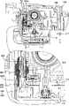
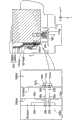
图1是表示作为本发明的一个实施例的印刷装置的说明图。印刷装置是记录材料消耗装置的一个例子。记录材料消耗装置消耗记录材料来执行 记录。印刷装置1000包括副扫描输送机构、主扫描输送机构以及头驱动机构。副扫描输送机构包括未图示的送纸马达、以及被该送纸马达驱动的送纸辊10。副扫描输送机构使用送纸辊10在副扫描方向上运送印刷纸张P。主扫描输送机构使用托架马达2的动力使与驱动带1连接的托架3在主扫描方向上往复运动。托架3包括固定器4以及印刷头5。头驱动机构驱动印刷头5来喷出墨水。通过被喷出的墨水而在印刷纸张P上形成点。印刷装置1000还包括控制上述的各机构的主控制电路40。主控制电路40经由挠性电缆37与托架3连接。 FIG. 1 is an explanatory diagram showing a printing apparatus as an embodiment of the present invention. A printing device is an example of a recording material consumption device. The recording material consumption means consumes the recording material to perform recording. The
固定器4被构成为能够安装后述的多个墨盒,并配置在印刷头5上。在印刷装置1000通常使用时(印刷时),墨盒被安装在固定器4上,印刷装置1000包括墨盒。在图1所示的例子中,在固定器4上能够安装六个墨盒。例如,安装有黑色、青色、品红色、黄色、淡青色、淡品红色的六种墨盒。在印刷头5的上表面还配置有供墨针6,该供墨针6用于从墨盒向印刷头5供应墨水。在图1中,在固定器4上安装有一个墨盒100。 The
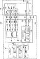
图2、图3是表示印刷装置1000和墨盒100的电结构的说明图。图2着眼于主控制电路40、托架电路500以及墨盒100的整体而被绘成。图3表示代表多个墨盒的一个墨盒100的结构。电结构对其他的墨盒也是一样的。 2 and 3 are explanatory diagrams showing the electrical configurations of the
主控制电路40和托架电路500被配置在印刷装置1000的内部,并且是为了执行印刷而控制印刷装置1000的各种机构的控制电路,以后将两者统称为印刷装置1000的控制部。另外,从配置在墨盒100上的设备来看,控制部成为外部的装置,因此在控制部和设备的动作的说明中,从设备来看,也有时称为外部装置。 The
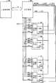
如图2所示,托架电路500与墨盒100之间由多个配线连接。多个配线包括重置信号线LR1、数据信号线LD1、时钟信号线LC1、电源线LCV、接地线LCS、第一传感器驱动信号线LDSN、以及第二传感器驱动信号线LDSP。五种配线LR1、LD1、LC1、LCV、LCS的每一个,分叉并与全部的墨盒100连接(总线连接)。传感器驱动信号线LDSN、LDSP对各墨盒100都分别设置。 As shown in FIG. 2 , the
如图3所示,墨盒100包括电路基板200以及传感器104。电路基板200包括作为设备的半导体存储装置203(以下也简称为“存储装置203”)以及七个端子210~270。电路基板200是配置有与印刷装置1000的控制部电连接的端子的连接体,用于将印刷装置1000的控制部和配置在墨盒100上的设备或传感器电连接。电源端子220、重置端子260、时钟端子270、数据端子240、以及接地端子230与存储装置203的电源端子接点Pvdd(以后称为电源接点)、重置端子接点Prst(以后称为重置接点)、时钟端子接点Psck(以后称为时钟接点)、数据端子接点Psda(以后称为数据接点)、接地端子接点Pvss(以后称为接地接点)分别电连接。作为存储装置203,可以采用各种存储器。在本实施例中,采用了基于在存储装置203的内部基于时钟信号生成的地址以字单位选择访问(读出和写入)对象的存储单元的存储器(例如,EEPROM或将强电介质用作存储单元阵列的存储器)。存储装置203存储与容纳在墨盒100中的墨水有关的信息。另外,作为存储装置203,至少具有存储数据(信息)的存储功能即可,除了存储功能以外也可以具有CPU等。例如也可以包括CPU和程序存储部。 As shown in FIG. 3 , the
传感器104是用于检测墨水余量的传感器。在本实施例中,作为传感器104,采用了通过两个电极来夹持压电体而成的压电元件。压电元件(传感器104)被固定在墨盒100的框体上。一旦对压电元件施加驱动电压,则压电元件会发生变形(该现象称为逆压电效果)。通过利用该逆压电效果,能够使压电元件强制地振动。并且,在停止驱动电压的施加后,可残留压电元件的振动。残留振动的频率表示与压电元件一起振动的周围的构造体(例如墨盒100的框体和墨水)的固有频率。残留振动的频率根据残留在墨盒100中的墨水量(传感器104的附近的墨水流道是否残留墨水)而变化。因此,可以根据残留振动的频率来确定墨水余量是否大于等于预定量。通过测定由压电效果产生的电压的振动频率来获取残留振动的频率。第一传感器端子210和第二传感器端子250分别与传感器104(压电元件)的一个电极和另一个电极电连接。另外,残留振动的振幅也根据墨水余量而变化。因此,也可以根据由压电效果产生的电压的变动振幅来 确定墨水余量是否大于等于预定量。 The
印刷装置1000包括接点机构400以及托架电路500。接点机构400和托架电路500被设置在托架3(图1)上。托架电路500被安装在设置于托架3上的控制基板上。控制基板经由挠性电缆37与主控制电路40电连接。 The
托架电路500具有存储器控制电路501、传感器驱动电路503以及七个端子510~570。电源端子520、重置端子560、时钟端子570、数据端子540以及接地端子530与存储器控制电路501电连接。接地端子530经由存储器控制电路501和主控制电路40接地(与印刷装置1000的地线连接)。这些端子520、530、540、560、570经由接点机构400(接触部件420、430、440、460、470)分别与墨盒100的端子220、230、240、260、270连接。即,当用户将电路基板200安装到印刷装置1000时,印刷装置1000与电路基板200的端子电连接。另外,接触部件420相当于图2的电源线LCV的一部分,接触部件460相当于重置信号线LR1的一部分,接触部件470相当于时钟信号线LC1的一部分,接触部件440相当于数据信号线LD1的一部分,接触部件430相当于接地线LCS的一部分。 The
存储器控制电路501经由这些端子来控制存储装置203,对存储装置203进行数据的读写。具体地说,电源电位(电源电压)VDD通过电源端子520从存储器控制电路501提供给存储装置203。重置信号RST通过重置端子560从存储器控制电路501提供给存储装置203。时钟信号SCK通过时钟端子570从存储器控制电路501提供给存储装置203。数据端子540被用于存储器控制电路501与存储装置203之间的数据信号SDA的传送(发送和接收)。接地电位VSS通过接地端子530从存储器控制电路501提供给存储装置203(墨盒100的接地端子230是在墨盒100被正确地(无位置偏差)安装在印刷装置1000(固定器4)上的状态下与印刷装置1000的地线导通的端子)。另外,电源电位VDD与印刷装置1000的接地电位(地线)不同。 The
另外,在本实施例中,对各墨盒100的存储装置203预先分配互不相同的ID号(识别号)。该ID号是存储器控制电路501用于确定被总线连 接的多个存储装置203的识别号。存储器控制电路501向数据信号线LD1提供表示作为控制对象的存储装置203的ID号的数据,并且提供表示指令的数据。与该ID号对应的存储装置203执行与指令相应的处理(例如,数据读取和数据写入)。与被指定了的ID号不同的ID号的存储装置203不进行对指令的响应,等待被指定自己的ID号(后面详述)。 In addition, in this embodiment, ID numbers (identification numbers) different from each other are allocated in advance to the
另外,在本实施例中,存储器控制电路501和存储装置203是以比在后述的墨水余量检测时施加给压电元件的电压低的电压(在本实施例中最大约3.3V)动作的低电压电路。另外,作为存储器控制电路501的结构,可以采用适合于存储装置203的各种结构。 In addition, in the present embodiment, the
托架电路500的第一传感器端子510和第二传感器端子550与传感器驱动电路503电连接。这些端子510、550经由接点机构400(接触部件410、450)分别与墨盒100的端子210、250连接(图3的接触部件450相当于图2的第二传感器驱动信号线LDSP的一部分,接触部件410相当于第一传感器驱动信号线LDSN的一部分)。传感器驱动电路503经由这些端子向传感器104施加电压,并且接收来自传感器104的输出信号(响应)。传感器驱动电路503包括盒体检测电路503a以及墨水余量检测电路503b。 The
盒体检测电路503a经由这些端子510、550在检查墨盒是否被安装在固定器4上时输出预定信号(电压)。并且,盒体检测电路503a通过经由端子510、550获取对被输出了的信号(电压)的响应,来检测电路基板200是否与印刷装置连接、即墨盒100是否被安装在印刷装置上。另外,墨水余量检测电路503b经由这些端子510、550输出驱动电压。并且,墨水余量检测电路503b通过经由端子510、550获取表示压电元件的电极之间的电压的波形的频率或振幅来检测墨水余量。后面详细叙述这些处理。另外,在本实施例中,传感器104是接收比存储装置203高的电压(在本实施例中最大约40V)的高电压电路。另外,作为盒体检测电路503a和墨水余量检测电路503b的结构,可以采用各种结构。例如,也可以采用组合逻辑电路而得到的结构。代替之,也可以使用计算机来构成传感器驱动电路503。另外,在本实施例中,托架电路500(包括传感器驱动电路 503)使用ASIC来构成。 The
托架电路500经由包括挠性电缆37(图1)的总线B与主控制电路40连接。托架电路500按照主控制电路40的指示而动作。另外,在本实施例中,印刷装置1000对应于多个墨盒的每个而具有接点机构400。即,六个墨盒100被安装在托架3(图1)上,因此六个接点机构400被设置在托架3上。另外,在本实施例中,一个托架电路500被六个墨盒100共同利用。托架电路500一个一个地处理多个墨盒100。存储器控制电路501利用ID号(识别号)来选择作为处理对象的一个存储装置203(后面详细叙述)。传感器驱动电路503通过设置在托架电路500上的未图示的开关电路来选择作为处理对象的一个传感器104。 The
主控制电路40是包括CPU和存储器(ROM、RAM等)的计算机。在存储器中存储有盒体检测模块M10、墨水余量检测模块M20以及存储器控制模块M30。以下,将这些模块M10~M30分别称为第一模块M10、第二模块M20、第三模块M30。这些模块M10~M30是通过CPU执行的计算机程序。以下,将CPU按照模块执行处理也简单地表述成“模块执行处理”。后面详细叙述各模块M10~M30的处理。 The
如图2、图3所示,主控制电路40经由总线B与托架电路500连接。主控制电路40经由该总线B将电源电位、接地电位、数据(例如表示从主控制电路向托架电路的处理要求的指令、该处理所需的数据、ID号等)提供给托架电路500。另外,托架电路500经由该总线B将数据提供给主控制电路40。 As shown in FIGS. 2 and 3 , the
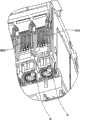
图4是托架3的立体图。图5是图4所示的托架3的一部分的放大图。在图4中,一个墨盒100被安装在托架3上。在图中,表示了X、Y、Z方向。以下,将X方向也称为“+X方向”,将X方向的逆方向也称为“-X方向”。对Y方向、Z方向也是一样的。 FIG. 4 is a perspective view of the
图中的Z方向表示了墨盒100的安装方向。通过墨盒100向Z方向的移动,墨盒100被安装在托架3上。在固定器4的底壁4wb(+Z方向的壁)配置有供墨针6。供墨针6向-Z方向突出。另外,在固定器4的前壁4wf(-Y方向的壁)配置有接点机构400。Y方向表示了与安装方向Z 垂直的方向。在本实施例中,六个供墨针6和六个接点机构400分别沿X方向(从-X向+X)排列配置。X方向是与安装方向Z和Y方向这两者垂直的方向。并且,六个墨盒在X方向上排列安装(省略图示)。 The Z direction in the figure indicates the installation direction of the
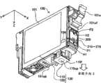
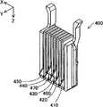
图6A和图6B表示墨盒100的立体图,图7A和图7B表示墨盒100的主视图。图中的X、Y、Z方向表示墨盒100安装在托架3(图4)上的状态下的方向。墨盒100的+Z方向上的面(与Z方向垂直的面。图6A中的底壁101wb)与托架3(图4)的底壁4wb相对。墨盒100的-Y方向上的面(与Y方向垂直的面。图6A中的前壁101wf)与托架3的接点机构400相对。 6A and 6B are perspective views of the
墨盒100包括框体101、传感器104以及电路基板200。在框体101的内部形成有容纳墨水的墨水室120。传感器104被固定在框体101的内部。框体101包括前壁101wf(-Y方向的壁)、底壁101wb(+Z方向的壁)以及后壁101wbk(+Y方向的壁)。前壁101wf与底壁101wb交叉(在本实施例中,实质上是正交)。电路基板200被固定在前壁101wf上。在电路基板200的外表面(与印刷装置1000的接点机构400(图4)相对的面)形成有端子210~270。供墨口被配置在底壁的、前壁101wf和与之相对的后壁wbk(+Y方向的壁)中更靠近前壁的位置处。 The
在前壁101wf上形成有两个突起P1、P2。这些突起P1、P2在-Y方向上突出。在电路基板200上形成有分别接受这些突起P1、P2的孔H1以及缺口H2。突起P1、P2和孔H1、缺口H2用于防止电路基板安装到墨盒时的安装位置偏差,成为位置偏差防止部。孔H1被形成在电路基板200的下端(+Z方向的端)的中央,缺口H2被形成在电路基板200的上端(-Z方向的端)的中央。在电路基板200被安装在了前壁101wf上的状态下,突起P1、P2分别插入到孔H1、缺口H2中。通过孔H1与突起P1接触,缺口H2与突起P2接触,从而前壁101wf上的电路基板200的位置偏差被限制。在电路基板200被安装在前壁101wf上之后,这些突起P1、P2的顶端被挤压。即,对突起P1、P2的顶端加热并挤压该顶端,通过热铆接使突起P1、P2和电路基板贴紧。由此,电路基板200被固定在前壁101wf上。 Two protrusions P1, P2 are formed on the front wall 101wf. These protrusions P1 and P2 protrude in the -Y direction. A hole H1 and a notch H2 for respectively receiving these protrusions P1 and P2 are formed in the
另外,在前壁101wf上设置有配合突起101e。通过配合突起101e和固定器4(图4)的配合,能够防止墨盒100意想不到地从固定器4上脱落。 In addition, an
在底壁101wb上形成有作为记录材料供应口的墨水供应口110。墨水供应口110与墨水室120连通。将墨水供应口110和墨水室120的整体称为“墨水容纳部130”。墨水供应口110的开口110op通过薄膜110f进行密封。由此,能够防止墨水从墨水供应口110泄漏。通过将墨盒100安装在托架3(图4)上,供墨针6戳破封口(薄膜110f)而插入到墨水供应口110中。容纳在墨水室120(图6A)中的墨水经由供墨针6被供应给印刷装置1000。另外,图7B所示的中心线CL表示墨水供应口110的中心轴。在墨盒100被正确地(无位置偏差)安装在托架3上的状态下,中心线CL与供墨针6的中心轴相同。另外,墨盒100相当于墨水供应系统(更一般地说,为记录材料供应系统)。 An
图8是表示将墨盒100安装到托架3上的情况的说明图。图9是表示墨盒100被安装在托架3上的状态的说明图。这些图表示了墨盒100和托架3的截面。该截面是与X方向垂直的截面。 FIG. 8 is an explanatory diagram showing a state where the
当安装墨盒100时,首先在固定器4的上方向(-Z方向)上以墨水供应110与供墨针6相对的方式配置墨盒100。然后,通过使墨盒100在安装方向Z上移动,墨盒100被安装在固定器4上。由此,墨盒100的配合突起101e与固定器4的配合突起4e配合。另外,供墨针6被插入到墨水供应口110。在墨水供应口110的开口110op上设置有环状的密封部件112。密封部件112由橡胶等弹性材料形成,与供墨针6接触来防止漏墨。这样,密封部件112形成墨水供应口110(开口110op)与供墨针6的接触部分。 When installing the
如图8所示,在密封部件112的上游侧配置有阀体113。该阀体113通过未图示的弹簧向密封部件112施力。当墨盒100从固定器4上取下时,阀体113与密封部件112接触,从而关闭墨水供应口110。由此,即使是墨盒100被暂时安装在固定器4上薄膜110f被戳破了之后,墨盒100从固定器4上被取下的情况下,能够降低墨水从墨水供应口110泄漏的可 能性。 As shown in FIG. 8 , a
如图9所示,在墨盒100被安装在固定器4上的状态下,在电路基板200的前方向(-Y方向)上配置有接点机构400。并且,在接点机构400的-Y方向上配置有基板500b。在基板500b上安装有托架电路500。电路基板200的端子210~270和托架电路500的端子510~570分别通过接点机构400电连接(后面详述)。另外,安装方向Z也相当于电路基板200被安装(连接)在印刷装置1000上时的安装方向。 As shown in FIG. 9 , in the state where the
一旦墨盒100被安装在固定器4上,则供墨针6推起阀体113,阀体113离开密封部件112。由此,墨水室120和供墨针6连通,墨水室120内的墨水能够供应给印刷装置1000。 Once the
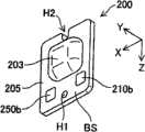
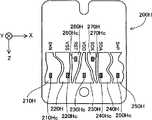
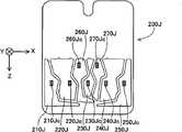
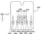
图10A、图10B是电路基板200的立体图。图10C表示沿Y方向(从-Y向+Y)观察电路基板200的主视图,图10D表示沿-X方向(从+X向-X)观察电路基板200的侧视图,图10E表示沿-Y方向(从+Y向-Y)观察电路基板200的背面图。图中的X、Y、Z方向表示在墨盒100安装在托架3(图4)上的状态下的方向。 10A and 10B are perspective views of the
电路基板200在作为绝缘体的基板205上配置有端子210~270以及存储装置203。基板205包括:存储装置203,被固定在基板205的里侧BS;以及端子210~270,被形成在基板205的表侧FS。基板205是与Y方向垂直的平板,其形状是具有与X方向平行的边和与Z方向平行的边的近似矩形形状。表侧FS表示前方向(-Y方向)的表面,里侧BS表示后方向(+Y方向)的表面。孔H1和缺口H2被形成在基板205上。端子220、230、240、260、270通过未图示的导电路分别与存储装置203的接点Pvdd、Pvss、Psda、Prst、Psck(图3)连接。导电路例如可包括开设在基板205上的通孔、形成在基板205的表面和内部的导电图案以及连接该导电图案和存储装置203的接点的接合线。另外,在本实施例中,被固定在基板205上的存储装置203的表面由树脂RC覆盖。 In the
图10C表示电路基板200的表侧FS。七个端子210~270分别被形成为近似矩形形状。这些端子210~270被配置成形成沿与墨盒100安装到固定器4的方向Z垂直的X方向(从-X向+X)延伸的两条线L1、L2。第 一线L1是近似垂直于插入方向Z的、通过多个接触部210c~250c形成或规定的假想直线(线段),所述多个接触部210c~250c包括第一传感器端子210与接触部件410接触的接触部210c以及第二传感器端子250与接触部件450接触的接触部250c。第二线L2是近似垂直于插入方向Z的、通过重置端子260与接触部件460接触的接触部260c以及时钟端子270与接触部件470接触的接触部270c形成或规定的假想直线(线段)。第一线L1是配置在关于安装方向Z的前头侧(安装时的移动方向的、对其他线(这里为第二线L2)的前头侧)的线。另外,在墨盒100(图8、图9)被正确地(无位置偏差)安装在固定器4上的状态下,多条线中最靠近墨水供应口110(开口110op)的线是第一线L1。具有形成第一线L1的接触部的端子从图中的左侧(-X方向的端)依次是第一传感器端子210、电源端子220、接地端子230、数据端子240、第二传感器端子250。形成第二线L2的端子从图中的左侧依次是重置端子260、时钟端子270。另外,可以省略两个传感器端子210、250。在此情况下,形成第一线L1的接触部的端子成为与存储装置203连接的端子中的电源端子220、接地端子230以及数据端子240这三个端子。如该例那样,第一线L1也可以通过与存储装置203连接的端子的一部分或全部的端子的接触部来形成。 FIG. 10C shows the front side FS of the
图10E表示电路基板200的里侧BS。在里侧BS形成有两个端子210b、250b。这些端子210b、250b分别与表侧FS的端子210、250导通。传感器104的一个电极与端子210b连接,传感器104的另一个电极与端子250b连接。 FIG. 10E shows the backside BS of the
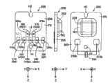
图11A是沿-Y方向(从+Y向-Y)观察接点机构400的背面图,图11B是沿-X方向(从+X向-X)观察接点机构400的侧视图。另外,图12是接点机构400的立体图。接点机构400包括支承部件400b以及七个接触部件410~470。在支承部件400b上沿X方向(从-X向+X)交替地排列形成有第一缝401和第二缝402。第二缝402相对于第一缝401向-Z方向偏移。在这些缝401、402中以与电路基板200的端子210~270(图10C)对应的方式而嵌入有接触部件410~470。接触部件410~470分别具有导电性和弹性。另外,+X侧的第二缝402a和-X侧的 第二缝402b未被利用,因此也可以省略。 11A is a rear view of the
如图11B所示,接触部件410~470的一端从支承部件400b在+Y方向上突出。该突出的一端被向电路基板200施力,并与电路基板200的端子210~270中的对应的端子接触。图11A表示接触部件410~470中的、与端子210~270接触的部分410c~470c。这些接触部410c~470c作为用于电连接印刷装置1000和电路基板200的端子210~270的装置侧端子而发挥功能。以下,将这些接触部410c~470c也称为装置侧端子410c~470c。 As shown in FIG. 11B , one ends of the
另一方面,如图11B所示,接触部件410~470的另一端从支承部件400b向-Y方向突出。该突出的另一端被向基板500b施力,与设置于基板500b的端子510~570(托架电路500的端子510~570)中的对应的端子接触。虽然省略了图示,但是托架电路500的端子510~570也与图10C所示的端子210~270同样地配置。另外,这些端子510~570被形成在基板500b的与接点机构400相对的面上。 On the other hand, as shown in FIG. 11B , the other ends of the
图13A~图13E是表示安装墨盒100(图8)时的、接触部件410~470与端子210~270的接触的说明图。图13A~图13E表示沿-X方向(从+X向-X)观察的接点机构400和电路基板200。当安装时,电路基板200在安装方向Z上移动。电路基板200和接点机构400的位置关系以图13A~图13E的顺序变化。 13A to 13E are explanatory diagrams showing contact between the
首先,如图13B所示,电路基板200的基板205的下端LE(+Z方向的端)与相对于接触部件410~450向-Z方向偏移配置的两个接触部件460、470接触。并且,通过基板205向+Z方向移动,接触部件460、470被推向-Y方向。接触部件460~470具有弹性,接触部460c、470c向+Y方向被施力。因此,在接触部件460、470(接触部460c、470c)与基板205的表侧FS相接的状态下,基板205向+Z方向移动。 First, as shown in FIG. 13B , the lower end LE (the end in the +Z direction) of the
接着,如图13C所示,基板205的下端LE与向+Z方向偏移配置的五个接触部件410~450接触。这些接触部件410~450也具有弹性,接触部410c~450c向+Y方向被施力。因此,在接触部件410~450(接触部410c~450c)与基板205的表侧FS相接的状态下,基板205向+Z方向移 动。图13D表示基板205从图13C进一步向+Z方向移动的状态。图13D的状态是端子230在接触部件460与接触部件470之间移动的状态。 Next, as shown in FIG. 13C , the lower end LE of the
最后,如图13E所示,墨盒100的安装完成。在该状态下,接触部件410~470(接触部410c~470c)分别与电路基板200的端子210~270接触。 Finally, as shown in Fig. 13E, the installation of the
图13E表示两个距离Ds1、Ds2。第一距离Ds1表示接触部件410~450擦过基板205的表侧FS上的距离。第二距离Ds2表示接触部件460、470擦过基板205的表侧FS上的距离。如图所示,第一距离Ds1<第二距离Ds2。这样,对于与配置在安装方向Z的前头位置(前头侧)的第一线L1(图10C)对应的接触部件410~450,与其他的接触部件460、470相比,擦过表侧FS上的距离短。因此,与其他的接触部件460、470相比,表侧FS上的灰尘等异物难以附着在接触部件410~450上。即,与其他的接触部件460、470相比,接触部件410~450与端子210~250之间的连接不良的可能性小。 Fig. 13E shows two distances Ds1, Ds2. The first distance Ds1 represents the distance on the front side FS of the
以上说明的结构对全部的墨盒是通用的。 The structure described above is common to all ink cartridges. the
A2.盒体检测 A2. Box inspection
图14是表示盒体的检测处理的顺序的流程图。该处理是由印刷装置1000确认是否安装有墨盒的处理。该处理通过盒体检测(第一)模块M10和托架电路500(传感器驱动电路503)而被执行(图3)。图14的顺序是与一个墨盒有关的处理。第一模块M10和托架电路500对假设要安装到固定器4(图4)的全部的墨盒的每一个执行该处理。由此,第一模块M10确认全部(六个)的墨盒的安装。另外,第一模块M10也可以以各种时机来执行该处理。例如,可以定期地执行处理,也可以在满足了预定的条件时(例如,印刷装置1000的电源被接通时或者墨盒100被更换了时或者开始印刷时)执行处理,还可以根据用户的指示来执行处理。 FIG. 14 is a flowchart showing the procedure of cassette detection processing. This process is a process in which the
在最初的步骤S100中,第一模块M10从作为检查对象的墨盒的传感器端子510、550输出信号(电压)。具体地说,第一模块M10向盒体检测电路503a提供信号输出的指示。该指示包括墨盒的ID号。盒体检测电路503a按照指示切换开关电路,以选择与ID号对应的传感器端子510、 550,并向被选出的传感器端子510、550输出信号(电压)。当墨盒100被安装了时,向传感器104的两个电极之间施加电压。由此,传感器104被充电。 In the first step S100, the first module M10 outputs a signal (voltage) from the
在接下来的步骤S110中,第一模块M10利用传感器端子510、550来获取响应信号(电压)。具体地说,第一模块M10向盒体检测电路503a提供信号(电压)获取的指示。盒体检测电路503a按照指示来停止电压施加,并且测定两个传感器端子510、550之间的电压。盒体检测电路503a将测定出的电压通知给第一模块M10。 In the next step S110, the first module M10 uses the
在接下来的步骤S120中,第一模块M10判断被测定出的电压是否高于预定的阈值。当墨盒100被安装了时,测定被充电了的传感器104的电压。该测定电压的绝对值(称为第一电压)比0高。当墨盒100未被安装时,测定电压大致为0。阈值预先在实验中被设定在0与第一电压之间。因此,当测定电压的绝对值高于阈值时,第一模块M10判断为墨盒100被安装了(步骤S130)。当测定电压的绝对值小于等于阈值时,第一模块M10判断墨盒100未被安装(步骤S140)。然后,第一模块M10结束处理。 In the next step S120, the first module M10 determines whether the measured voltage is higher than a predetermined threshold. When the
当至少一个安装位置未安装墨盒时,第一模块M10优选执行与盒体的未安装有关的处理。作为这样的处理,例如可以采用保留印刷的处理或者将盒体的未安装通知给用户的处理。 When the ink cartridge is not installed in at least one installation position, the first module M10 preferably performs processing related to the non-installation of the cartridge body. As such a process, for example, a process of saving printing or a process of notifying the user that the cartridge has not been installed can be employed. the
A3.存储器控制: A3. Memory control:
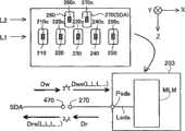
图15是表示本实施例中的存储装置203的结构的说明图。存储装置203是包括输入输出电路IOC、逻辑模块MLM、非易失性的存储单元阵列MCA、五个接点(输入输出端子)Pvdd、Prst、Psck、Psda、Pvss的半导体芯片。逻辑模块MLM包括ID比较部MLM1、地址生成部MLM2、读写控制部MLM3。逻辑模块MLM根据来自外部装置(例如,图3的印刷装置1000的控制部(主控制电路40和托架电路500的整体))的指示来执行对存储单元阵列MCA的数据的写入以及从存储单元阵列MCA的数据的读取(后面详述)。输入输出电路IOC包括五条线Lvdd、Lrst、Lsck、Lsda、Lvss、三个缓冲电路MBrst、MBsck、MBsda以及保护电路 PC。接点Pvdd、Prst、Psck、Psda、Pvss分别通过线Lvdd、Lrst、Lsck、Lsda、Lvss与逻辑模块MLM连接。电源线Lvdd是用于接收电源电位VDD的线。重置线Lrst是用于接收重置信号RST的线。在重置线Lrst上设置有第一缓冲电路MBrst。时钟线Lsck是用于接收时钟信号SCK的线。在时钟线Lsck设置有第二缓冲电路MBsck。数据线Lsda是用于发送和接收数据信号SDA的线。在数据线Lsda上设置有第三缓冲电路MBsda。接地线Lvss是用于接收接地电位VSS的线。接点Pvdd、Prst、Psck、Psda、Pvss分别与电路基板200的端子220、260、270、240、230电连接。 FIG. 15 is an explanatory diagram showing the configuration of the
保护电路PC保护存储装置203的内部电路(包括逻辑模块MLM和存储单元阵列MCA)免受对接点的静电等的异常输入带来的影响。在本实施例中,保护电路PC包括保护二极管D1~D6。三个二极管D1、D3、D5的阴极与电源接点Pvdd(电源线Lvdd)连接。这些二极管D1、D3、D5的阳极分别与接点Prst、Psck、Psda(线Lrst、Lsck、Lsda)连接。三个二极管D2、D4、D6的阳极与接地接点Pvss(接地线Lvss)连接。这些二极管D2、D4、D6的阳极分别与接点Prst、Psck、Psda(线Lrst、Lsck、Lsda)连接。 The protection circuit PC protects the internal circuits of the storage device 203 (including the logic module MLM and the memory cell array MCA) from abnormal input such as static electricity to the contacts. In this embodiment, the protection circuit PC includes protection diodes D1-D6. The cathodes of the three diodes D1, D3, and D5 are connected to the power supply contact Pvdd (power supply line Lvdd). Anodes of these diodes D1, D3, D5 are connected to contacts Prst, Psck, Psda (lines Lrst, Lsck, Lsda), respectively. The anodes of the three diodes D2, D4, and D6 are connected to the ground contact Pvss (ground line Lvss). Anodes of these diodes D2, D4, D6 are connected to contacts Prst, Psck, Psda (lines Lrst, Lsck, Lsda), respectively. the
图16是表示存储装置203的动作的时序图。在图中示出了存储装置203(图15)的接点上的信号(电源电位VDD、重置信号RST、时钟信号SCK以及数据信号SDA)以及存储装置203的动作。在本实施例中,如图16所示的图那样来执行从存储装置203的存储单元阵列MCA读取数据以及对存储单元阵列MCA的写入数据这两者。在图中,H电平表示高电位(约3.3V),L电平表示低电位(0V)(这些电位的基准是接地电位VSS)。另外,表示信号的符号下所表示的箭头表示信号(数据)流动的方向。向右的箭头表示从存储器控制电路501(图3)向存储装置203的流动,向左的箭头表示从存储装置203向存储器控制电路501的流动。数据信号SDA可以在双向上流动。 FIG. 16 is a timing chart showing the operation of the
在本实施例中,对存储装置203(图15:存储单元阵列MCA)的访问是顺序访问。作为访问对象的存储器地址基于时钟信号SCK从预定的开 始地址以预定的顺序被更新。在本实施例中,以行单位统一执行对存储单元阵列的写入、从存储单元阵列的读取,因此存储器地址成为行指定地址。存储单元从存储单元阵列MCA的第0行一个一个地依次被访问。一个行(相当于一个字)的数据大小是n比特(n为1以上的整数。例如n=32)。地址生成部MLM2每当接收时钟信号SCK的n个时钟脉冲,则以第0行、第1行、第2行…的顺序来更新作为访问对象的存储器地址。另外,在第0行中预先存储有存储装置203的ID号。在本实施例中,ID号以3比特表示。另外,行的存储单元阵列上的物理配置也可以不按照行的访问顺序。 In this embodiment, access to the storage device 203 (FIG. 15: memory cell array MCA) is sequential access. The memory addresses to be accessed are updated in predetermined order from a predetermined start address based on the clock signal SCK. In the present embodiment, writing to the memory cell array and reading from the memory cell array are collectively performed on a row-by-row basis, so the memory address becomes the row designation address. The memory cells are sequentially accessed one by one from
当访问存储装置203(图15)时,存储器控制电路501(图3)首先将电源电位VDD设定为H电平。接着,存储器控制电路501将重置信号RST设定为H电平。在本实施例中,在重置信号RST处于H电平(与接地电位VSS不同的预定的电平)的状态下,存储装置203与时钟信号SCK同步地进行动作。当重置信号RST是H电平以外的电平(例如,L电平(与接地电位VSS相同的电位))时,存储装置203停止动作。存储器控制电路501通过过后将重置信号RST从H电平改变为L电平,能够重置全部的存储装置203的动作(后面详述)。 When accessing the memory device 203 (FIG. 15), the memory control circuit 501 (FIG. 3) first sets the power supply potential VDD to H level. Next, the
接着,存储器控制电路501(图3)将时钟信号SCK提供给电路基板200(图15)的时钟端子270。另外,存储器控制电路501与时钟信号SCK同步地将n比特量的数据信号SDA提供给数据端子240。n比特的数据中的最初的3比特表示作为访问对象的存储装置203的ID号。接下来的1比特表示指令。指令是读数据(R)和写数据(W)中的某一者(例如,L电平表示R,H电平表示W)。剩下的比特是伪数据。 Next, the memory control circuit 501 ( FIG. 3 ) supplies the clock signal SCK to the
在接收最初的n个时钟脉冲CP1的期间,逻辑模块MLM(图15)执行以下的处理。地址生成部MLM2(图15)生成表示第0行的存储器地址。读写控制部MLM3从存储单元阵列MCA读取被生成了的地址的数据(第0行数据)(图16:步骤10)。接着,ID比较部MLM1判断从存储单元阵列MCA读取出的自己的ID号是否与由存储器控制电路501(图3)指定的ID号相同(步骤S20)。当自己的ID号与被指定了的ID号不 同时,逻辑模块MLM停止处理,并改变到监视重置信号RST的动作模式(待命)。当自己的ID号与被指定了的ID号相同时,逻辑模块MLM继续进行处理。通过与ID号相应的处理的切换,通过存储器控制电路501指定了的存储装置203执行与存储器控制电路501的指示相应的处理。在接下来的步骤S30中,读写控制部MLM3判断由数据信号SDA指定了的指令是否是读数据(R)和写数据(W)中的一个。在接收到最初的n个时钟脉冲之后,逻辑模块MLM开始与指令相应的处理。 While receiving the first n clock pulses CP1, the logic module MLM (FIG. 15) executes the following processing. The address generator MLM2 (FIG. 15) generates a memory address indicating the 0th row. Read/write control unit MLM3 reads data (0th row data) at the generated address from memory cell array MCA (FIG. 16: STEP 10). Next, ID comparison unit MLM1 judges whether or not its own ID number read from memory cell array MCA is the same as the ID number designated by memory control circuit 501 (FIG. 3) (step S20). When its own ID number is different from the assigned ID number, the logic module MLM stops processing and changes to the action mode (standby) for monitoring the reset signal RST. When its own ID number is the same as the assigned ID number, the logic module MLM continues processing. By switching the processing corresponding to the ID number, the
当指令是读数据时,逻辑模块MLM(图15)与时钟信号SCK同步地执行步骤S41~S4k的处理。如上所述,地址生成部MLM2(图15)每当接收到n个时钟脉冲时,将存储器地址从第0行一行一行地增加。读写控制部MLM3从存储单元阵列MCA读取由地址生成部MLM2指定了的地址的数据。然后,读写控制部MLM3与时钟信号SCK同步地利用数据信号SDA来1比特1比特地输出读取出的数据。例如,读写控制部MLM3根据第二组n个时钟脉冲CP2来输出第一行的数据(S41)。详细地说,当为第二组n个时钟脉冲CP2中的最初的时钟脉冲时,读写控制部MLM3读取存储单元阵列的第一行,与n个时钟脉冲CP2的各个时钟脉冲同步,将读取出的n比特的数据输出给存储器控制电路501。存储器控制电路501(图3)与时钟信号SCK同步,1比特1比特地接收被存储在存储单元阵列MCA中的第1行~第k行的数据(k为1以上的整数)。在图16的实施例中,在接收到第k行的数据之后,存储器控制电路501停止提供时钟信号SCK。 When the command is to read data, the logic module MLM (FIG. 15) executes the processing of steps S41 to S4k in synchronization with the clock signal SCK. As described above, the address generator MLM2 ( FIG. 15 ) increments the memory address from
当指令是写数据(W)时,逻辑模块MLM(图15)与时钟信号SCK同步地执行步骤S51~S5k的处理。存储器控制电路501(图3)利用数据信号SDA与时钟信号SCK同步地将用于存储到存储单元阵列MCA中的数据1比特1比特地提供给逻辑模块MLM。读写控制部MLM3将接收到的数据存储在存储单元阵列MCA的由地址生成部MLM2指定的地址中。例如,读写控制部MLM3与第二组n个时钟脉冲CP2同步地将接收到的数据存储在存储单元阵列MCA的第1行(S51、S51w)。在图16的实施例中,在数据存储到第k行的存储单元(S5kw)之后,存储器控制电路 501停止提供时钟信号SCK。 When the command is to write data (W), the logic module MLM (FIG. 15) executes the processing of steps S51 to S5k in synchronization with the clock signal SCK. The memory control circuit 501 ( FIG. 3 ) supplies data for storing in the memory cell array MCA to the logic module MLM bit by bit using the data signal SDA in synchronization with the clock signal SCK. Read/write control unit MLM3 stores the received data in the address specified by address generation unit MLM2 in memory cell array MCA. For example, the read/write control unit MLM3 stores the received data in the first row of the memory cell array MCA in synchronization with the second group of n clock pulses CP2 ( S51 , S51w ). In the embodiment of FIG. 16, after data is stored in the memory cell (S5kw) of the k-th row, the
另外,如后面所述,在固定器4内墨盒100的位置有可能偏离正确的位置。假定由于这样的位置偏差,电路基板200(图2)的数据端子240离开接点机构400的接触部件440。这里,当向存储装置203(图15)正常地提供了电源电位VDD、重置信号RST以及时钟信号SCK时,逻辑模块MLM可将基于数据线Lsda的电位的数据(错误的数据)写入到存储单元阵列MCA中(数据线Lsda的电位例如可与接地线Lvss相同)。不限于这样的原因,由于各种原因,存储装置203可发生误动作或者无法动作(后面详述)。 In addition, as will be described later, the position of the
在停止提供时钟信号SCK之后,存储器控制电路501(图3)将重置信号RST从H电平改变为L电平。由此,全部的存储装置203重置自己的动作。具体地说,地址生成部MLM2将存储器地址重置为第0行。另外,逻辑模块MLM在接下来接收到重置信号RST(H电平)、时钟信号SCK以及数据信号SDA时执行从图16的步骤S10起的处理。另外,存储器控制电路501在将重置信号RST设定为L电平之后,将电源电位VDD设定为L电平。由此,全部的存储装置203停止动作。 After the supply of the clock signal SCK is stopped, the memory control circuit 501 ( FIG. 3 ) changes the reset signal RST from H level to L level. As a result, all
另外,存储器控制电路501(图3)按照存储器控制(第三)模块M30的指示而动作。第三模块M30针对被安装在固定器4(图4)中的六个墨盒100的每一个访问存储装置203。作为存储在存储装置203中的信息,可以采用与容纳在墨盒100中的墨水有关的各种信息。例如,可以采用表示墨水的种类的信息。第三模块M30从存储装置203读取墨水种类信息,并确认安装了恰当的墨盒100。另外,也可以采用墨盒100被安装到印刷装置1000上之后的墨水消耗量(例如,点数)。第三模块M30在印刷时、执行喷嘴清洁后、用户向印刷装置1000输入了电源关闭的指示时等更新存储在存储装置203中的墨水消耗量即可。这样一来,第三模块M30通过从存储装置203读出墨水消耗量,能够估计墨水余量。另外,第三模块M30以各种时机来访问存储装置203。 In addition, the memory control circuit 501 (FIG. 3) operates in accordance with instructions from the memory control (third) module M30. The third module M30 accesses the
B.实施例的结构 B. Structure of the embodiment
以上说明的第一实施例具有各种结构(features)。以下,对它们的结 构进行说明。 The first embodiment explained above has various features. Hereinafter, their structures will be described. the
B1.结构1: B1. Structure 1:
本实施例具有以下的结构。 This embodiment has the following structure. the
向存储装置203提供电源电位VDD的电源端子220的接触部220c被配置在第一线L1上(图10C)。存储装置203经由该电源端子220的接触部220c来接受电源电位VDD。 The
这里,第一线L1是相对于其他的线(在本实施例中为第二线L2)被配置在前头位置(前头侧)的线。前头位置表示墨盒100被定向地安装到印刷装置1000时的前头位置。即,前头位置(前头侧)是安装方向Z的前头位置(前头侧)。 Here, the first line L1 is a line arranged at the front position (on the front side) with respect to the other lines (the second line L2 in this embodiment). The leading position indicates the leading position when the
接着,对优点进行说明。图17A和图17B是表示被安装了的墨盒100在固定器4内的位置偏差的说明图。图17A、图17B表示墨盒100与固定器4的截面(与X方向垂直的截面)。固定器4的供墨针6插入到墨盒100的墨水供应口110。因此,墨盒100的墨水供应口110被固定在固定器4的供墨针6上。结果,墨盒100可围绕墨水供应口110摆动。另外,在墨水供应口110的开口110op处,密封部件112与供墨针6接触。因此,墨盒100的运动的中心MC处于中心线CL上的密封部件112和供墨针6接触部分的附近位置。 Next, advantages will be described. 17A and 17B are explanatory diagrams showing positional deviation of the mounted
图17A、图17B表示墨盒100相对于Z轴向+Y方向倾斜的状态。这样倾斜的状态是由于各种原因而引起的。例如,当用户将墨盒100安装到固定器4(印刷装置1000)上时,有时墨盒100会在倾斜的状态下安装到固定器4上。另外,由于墨盒的图心CF以中心线CL作为基准处于+Y侧,从而墨盒的端子210~270容易向离开接触部件410~470的方向倾斜。对这方面后面详述。 17A and 17B show a state where the
图17A表示第一线L1的接触部210c~250c的移动距离da。图中的角度AG表示以墨水供应口110为中心的墨盒100的斜度(旋转角度)。第一距离Ra表示墨水供应口110(旋转中心MC)与接触部210c~250c的距离。 FIG. 17A shows the movement distance da of the
图17B表示第二线L2的接触部260c、270c的移动距离db。第二距离 Rb表示墨水供应口110(旋转中心MC)与接触部260c、270c的距离。墨盒100的旋转角度是与图17A相同的角度AG。 FIG. 17B shows the movement distance db of the
当角度AG大时,接触部210c~270c可从接触部件410~470离开。这里,第一线L1与第二线L2相比难以离开接触部件。其理由如下。在本实施例中,开口110op与多个端子210~270的多个接触部210c~270c相比,被配置在安装方向Z侧(图7A和图7B、图17A和图17B)。另外,第一线L1相对于其他的线(在本实施例中为第二线L2)被配置在安装方向Z的前头侧(在本实施例中,也可以说是多条线中的最靠近墨水供应口110的开口110op的线是第一线L1(图7))。即,第一距离Ra比第二距离Rb短。这里,当角度AG相同时,第一线L1与接触部件410~450的距离(第一移动距离da)比第二线L2与接触部件460、470的距离(第二移动距离db)短。另外,“开口110op与接触部210c~270c相比被配置在安装方向Z侧”意味着在与安装方向Z平行的方向的位置上,开口110op的位置与接触部210c~270c的每一个的位置相比处于安装方向Z侧。 When the angle AG is large, the
图18是接触部210c~270c的附近的放大图。图18表示图17A、图17B那样墨盒100倾斜了的状态。如图所示,随着角度AG的增大,第二线L2比第一线L1先从接触部件离开。 FIG. 18 is an enlarged view of the vicinity of the
这样,设置在电路基板200上的多条线L1、L2中的、与接触部件连接不良的可能性最小的线是第一线L1。因此,优选将设置在电路基板200上的多个接触部中的、由于接触不良而引起的不良情况的严重性高的接触部配置在第一线L1上。因此,在本实施例中,用于电源电位VDD的接触部220c被配置在第一线L1上(图10C)。 Thus, among the plurality of lines L1 , L2 provided on the
图19是表示比较例的说明图。在图中示出了电路基板的端子210~270以及存储装置203。在图19的结构中,用于电源电位VDD的接触部被配置在第二线L2(接触部270c),用于重置信号RST的接触部和用于数据信号SDA的接触部被配置在第一线L1上(接触部230c、240c)。具体地说,电源接点Pvdd与端子270连接,重置接点Prst、数据接点Psda分别与端子230、240连接。 FIG. 19 is an explanatory diagram showing a comparative example. The figure shows the
在图19的结构中,假定墨盒倾斜,第二线L2与接触部件460、470(图18)的接触断开。并且,假定在该状态下存储器控制电路501(图3)访问存储装置203(图16)。在该情况下,通过端子270向存储装置203提供的电源电位VDD被切断。代替之,重置信号RST通过保护二极管D1被提供给存储装置203的电源线Lvdd。但是,被供应的电压与重置信号RST相比低了保护二极管D1的正向电压(例如,0.6V)。 In the structure of FIG. 19, assuming that the ink cartridge is tilted, the contact of the second line L2 with the
这里,假定存储装置203的动作电压的允许范围为2.7V~3.3V。在此情况下,从存储器控制电路501(图3)提供给端子230的重置信号RST的电压也可以是2.7V~3.3V。当重置信号RST的电压为3.3V时,向电源线Lvdd提供2.7V的电压。在该状态下,存储装置203可动作。但是,由于电源线Lvdd的电压靠近允许范围的下限,因此存储装置203的动作也可能变得不稳定。另外,当重置信号RST的电压低时(例如,2.7V),存储装置203也有时无法动作。在这样的状况下,逻辑模块MLM有可能无法生成对存储单元阵列MCA的正确的控制信号。例如,响应于写要求,逻辑模块MLM有可能将与正确的写数据Dw不同的错误的数据Dwe存储在存储单元阵列MCA中。另外,响应于读要求,逻辑模块MLM有可能输出与正确的读数据Dr不同的错误的数据Dre。这样,看起来正常的动作实际上可能是误动作。 Here, it is assumed that the allowable range of the operating voltage of the
因此,在本实施例中,向存储装置203提供电源电位VDD的接触部被配置在第一线L1上(接触部220c)。结果,能够降低由上述的动作电压的不稳定性引起误动作的可能性。 Therefore, in the present embodiment, a contact portion for supplying the power supply potential VDD to the
另外,如图13E所示,在本实施例中,关于与配置在安装方向Z的前头位置上的第一线L1(图10C)对应的接触部件410~450,与其他的接触部件460、470相比,擦过表侧FS上的距离短(Ds1<Ds2)。因此,第一线L1的连接不良的可能性比其他的线小。从该观点出发,也优选将由于连接不良而引起误动作的严重性高的接触部(例如,接受电源电位VDD的接触部)配置在第一线L1上。 In addition, as shown in FIG. 13E , in this embodiment, the
另外,当重置端子260和时钟端子270中的某一个产生了连接不良时,存储装置203被初始化或者存储装置203的动作停止,因此与产生了 电源端子220的连接不良的情况相比,写入错误的数据的可能性小。因此,在本实施例中,将这些端子260、270的接触部260c、270c配置在不是前头线的其他的线(在本实施例中为第二线L2)上。 In addition, when one of the
另外,在本实施例中,如图17A、图17B所示,在墨盒100的一个侧壁(前壁101wf)上设置有接触部210c~270c(端子210~270)。并且,墨水供应口110被设置在墨盒100的底壁101wb上。这里,墨水供应口110被配置在底壁101wb的偏向前壁101wf侧的位置处。具体地说,在本实施例中,从底壁101wb中的最靠近前壁101wf的第一端E1(与前壁101wf连接的位置)与第一端E1的相反侧的第二端E2(与后壁101wbk连接的位置)之间的中间位置IP来看,墨水供应口110被配置在前壁101wf侧。另外,安装方向Z与重力方向向下相同。其结果,墨盒100的图心CF以中心线CL(中心MC)为基准,处于+Y侧(与接点机构400所在的侧相反的一侧)。图心CF是从+X向-X观察墨盒100时的墨盒100的轮廓的图心。另外,中间位置IP与将图心CF沿安装方向Z投影到底壁101wb上的位置大致相同。根据以上的结构,墨盒100容易向接触部210c~270c离开接触部件410~470的方向倾斜。在这样的情况下,如果采用上述的结构1,则其优点显著。另外,墨水供应口110比第二端E2(后壁101wbk)靠近第一端E1(端子210~270),因此与墨水供应口110比第一端E1靠近第二端E2的情况相比,能够减小相对于相同角度AG的移动距离da、db。因此,能够减小墨盒100倾斜了时的、端子210~270(接触部210c~270c)与接触部件410~470的接触不良的可能性。 In addition, in this embodiment, as shown in FIGS. 17A and 17B ,
B2.结构2: B2. Structure 2:
本实施例还可以具有以下的结构。 This embodiment may also have the following structures. the
数据端子240的接触部240c被配置在第一线L1上(图10C),所述数据端子240从外部装置(印刷装置1000的控制部(主控制电路40和托架电路50的整体)接收数据信号SDA以及向外部(印刷装置1000的控制部)发送数据信号SDA。存储装置203经由该数据端子240的接触部240c接收数据信号SDA,并且发送数据信号SDA。 The
图20是表示与结构2不同的结构的说明图。在图中示出了电路基板的端子210~270以及存储装置203。在图20的结构中,用于数据信号SDA的接触部被配置在第二线L2上(接触部270c)。具体地说,数据接点Psda与端子270连接。 FIG. 20 is an explanatory diagram showing a structure different from the
在图20的结构中,假定墨盒发生倾斜,端子270和接触部件470(图18)的接触断开。并且,假定在该状态下存储器控制电路501(图3)访问存储装置203(图16)。在该状态下,通过端子270的数据信号SDA的双向的传送(发送和接收)被切断。因此,存储装置203可在接收到电源电位VDD、重置信号RST以及时钟信号SCK的情况下动作,但是无法正常地动作。例如,响应于写要求,存储装置203有可能存储与正确的写数据Dw不同的错误的数据Dwe。存储装置203在不与印刷装置1000的接触部件470取得电连接的情况下,基于依据离开了接触部件的数据接点Psda(图15:数据线Lsda)的电位的数据(错误的数据)而动作。数据线Lsda的电位例如可以是L电平。在此情况下,错误的数据Dwe是所有比特都被设定为L电平的数据。同样地,响应于读要求,由存储器控制电路501接收的数据有可能是与正确的读数据Dr不同的错误的数据Dre(例如,所有比特都被设定为L电平的数据)。这样,看起来正常的动作实际上可能是误动作。 In the structure of FIG. 20, assuming that the ink cartridge is tilted, the contact between the terminal 270 and the contact member 470 (FIG. 18) is broken. Also, assume that the memory control circuit 501 ( FIG. 3 ) accesses the storage device 203 ( FIG. 16 ) in this state. In this state, bidirectional transmission (transmission and reception) of the data signal SDA via the
因此,在本实施例中,用于发送和接收数据信号SDA的数据端子的接触部可以配置在第一线L1上(接触部240c)。结果,能够降低上述的误动作的可能性。 Therefore, in the present embodiment, the contact portion of the data terminal for transmitting and receiving the data signal SDA may be arranged on the first line L1 (the
B3.结构3: B3. Structure 3:
本实施例还可以具有以下的结构。 This embodiment may also have the following structures. the
用于接收时钟信号SCK的时钟端子270的接触部270c被配置在与第一线L1不同的线(在本实施例中为第二线L2)上(图10C)。 The
本实施例的存储装置203在时钟信号SCK的供应被切断的情况下停止动作。因此,在产生了时钟端子270的连接不良的情况下,与电源端子220和数据端子240产生连接不良的情况相比,向存储装置203写入错误的数据的可能性小。因此,如本实施例那样,如果将时钟端子270的接触 部270c配置在与第一线L1不同的线(例如第二线L2)上,则能够将多个接触部分散到多条线上,而不会提高向存储装置203写入错误数据的可能性。由此,与将多个接触部配置在一条线上的情况相比,能够缩短各线的长度(即,能够使装置小型化)。 The
B4.结构4: B4. Structure 4:
本实施例还可以具有以下的结构。 This embodiment may also have the following structures. the
用于接收重置信号RST的重置端子260的接触部260c被配置在与第一线L1不同的线(在本实施例中为第二线L2)上(图10C)。 The
本实施例的存储装置203在重置信号RST的供应被切断的情况下,存储装置203从重置接点输入的信号成为比高电平低的电位的信号,存储装置203停止动作或者存储装置203重置自身。因此,在产生了重置端子260的连接不良的情况下,与电源端子220和数据端子240产生了连接不良的情况相比,向存储装置203写入错误的数据的可能性小。因此,如本实施例那样,如果将重置端子260的接触部260c配置在与第一线L1不同的线(例如第二线L2)上,则能够将多个接触部分散到多条线上,而不会提高向存储装置203写入错误数据的可能性。由此,与将多个接触部配置在一条线上的情况相比,能够缩短各线的长度(即,能够使装置小型化)。 In the
B5.结构5: B5. Structure 5:
本实施例还可以具有以下的结构。 This embodiment may also have the following structures. the
多个接触部(210c~270c)被配置在同一平面上(图10C)。当沿与该平面垂直的方向(Y方向)(从+Y向-Y)将墨水供应口110的中心轴(中心线CL)投影到该平面上时,配置在距中心轴CL最远的位置处的接触部是传感器端子210、250的接触部210c、250c(图10C)。 A plurality of contact parts (210c to 270c) are arranged on the same plane (FIG. 10C). When the center axis (center line CL) of the
传感器端子210、250是印刷装置1000的主控制电路40和托架电路500将用于检测是否安装有墨盒100的信号提供给电路基板200的端子(图3)。另外,如图21所示,当墨盒100的位置偏移了时,距中心线CL远的位置处的位置偏移(d1、d5)比靠近中心线CL的位置处的位置偏移(d2、d3、d4)大。因此,即使是在靠近中心线CL的端子230与对应 的接触部430c正确地(无位置偏差)接触的情况下,距中心线CL远的端子210、250有时也不会与对应的接触部410c、450c接触。因此,如果在距中心线CL最远的位置处配置传感器端子210、250的接触部210c、250c,则能够降低与墨盒100的安装有关的误检测的可能性。例如,当墨盒100的位置偏移、安装不恰当时,能够降低错误地检测出“安装”的可能性。由于印刷装置1000的控制部(主控制电路40和托架电路500)具有用于检测墨盒100是否正确地安装在印刷装置1000上的功能、或者印刷装置的控制部具有用于检测自身和电路基板的端子是否正确连接的功能,因此传感器端子210、250也称为盒体安装检测端子。 The
另外,在安装检测用的两个接触部210c、250c之间配置有电源端子230的接触部230c,因此在安装检测被确认了的状态下,电源端子230的电连接也被达到的可能性高。结果,能够降低电源端子230的连接不良的可能性,因此能够降低利用经由端子的电连接时发生不良的可能性。 In addition, since the
另外,传感器端子210、250是与其他的端子220~240、260、270相比接受高的电压(被施加高的电压)的端子(图3)。如果将这样的端子210、250的接触部210c、250c配置在距中心线CL最远的位置,则这些接触部210c、250c被配置在端部,因此能够降低靠近接触部210c、250c的其他的接触部的数量。因此,能够降低可输出高的电压的接触部件410、450与不想接触的端子(例如,与存储装置203连接的端子)接触的可能性。这样的不想要的接触可在安装(或取下)墨盒100时产生。另外,不想要的接触可经由附着在电路基板200上的墨水或污物等产生。 In addition, the
另外,多个接触部210c~270c配置在近似平面上即可而无需一定配置在同一平面上。 In addition, the plurality of
B6.结构6: B6. Structure 6:
本实施例还可以具有以下的结构。 This embodiment may also have the following structures. the
包括传感器端子210、250的接触部210c、250c的线(第一线L1)是多条线中的最长的线(图10C)。 The line (first line L1 ) including the
这里,线的长度是各线上的接触部的位置处于最端部的两个接触部之间的长度。在图10C所示的例子中,是线L1、线L2的长度。 Here, the length of the line is the length between two contact portions where the position of the contact portion on each line is at the endmost portion. In the example shown in FIG. 10C, it is the length of the line L1 and the line L2. the
该结构表示了传感器端子210、250的接触部210c、250c之间的距离比其他的线的两端的距离长。由此,当电路基板200的位置偏差(墨盒100对固定器4(图4)的位置偏差)大时,两个接触部210c、250c的至少一个对接点机构400的位置偏差也大。另外,通过将接触部210c、250c配置在一条线的两端,能够降低靠近接触部210c的其他的接触部的数量和靠近接触部250c的其他的接触部的数量。另外,该结构6具有与上述的结构5相同的优点。即,能够降低与墨盒100的安装有关的误检测的可能性。另外,能够降低利用经由端子的电连接时发生不良的可能性。并且,能够降低可输出高的电压的接触部件410、450与不想接触的端子(例如,与存储装置203连接的端子)接触的可能性。 This structure shows that the distance between the
B7.结构7: B7. Structure 7:
用于第二线L2的接触部(260c、270c)的接触部件(460、470)在安装(或取下)墨盒100时有可能与电路基板200的前头线(第一线L1)的端子接触。因此,如果其他的线的接触部的总数比第一线L1的接触部的总数少,则能够降低印刷装置1000的接触部件与电路基板200的不想接触的端子接触的可能性。结果,能够降低电路基板200发生故障的可能性。这里,其他的线的总数也可以是2个以上。在此情况下,优选前头线的接触部的总数比其他的线的全体上的接触部的总数多。 The contact members (460, 470) of the contact portions (260c, 270c) for the second line L2 may come into contact with the terminals of the front line (first line L1) of the
另外,如在图17A和图17B、图18的结构1中所说明的那样,前头的第一线L1与其他的线相比,连接不良的可能性小。因此,如果增加第一线L1的接触部的总数,则能够降低多个接触部全体的连接不良的可能性。 In addition, as described in FIGS. 17A and 17B , and configuration 1 of FIG. 18 , the leading first line L1 is less likely to have poor connection than the other lines. Therefore, if the total number of contact portions of the first line L1 is increased, it is possible to reduce the possibility of poor connection of the entire plurality of contact portions. the
C.第二实施例: C. The second embodiment:
图22、图23是表示墨水供应系统(记录材料供应系统)的第二实施例的立体图。与图6A、图6B所示的实施例的区别仅在于:墨盒100的要素中墨水容纳部130(墨水供应口110和墨水室120的整体)与其他要素分离。印刷装置1000的结构与上述的第一实施例的结构相同。 22 and 23 are perspective views showing a second embodiment of the ink supply system (recording material supply system). The only difference from the embodiment shown in FIGS. 6A and 6B is that, among the elements of the
该墨水供应系统SI包括构造体100A(以下也称为“接合器100A”)以及墨水容纳部100B。墨水容纳部100B包括容纳墨水的框体101B以及 墨水供应口110。在框体101B的内部形成有容纳墨水的墨水室120B。墨水供应口110被形成在框体101B的底壁101Bwb(+Z方向的壁)上。墨水供应口110与墨水室120B连通。墨水供应口110的结构与上述的墨盒100的墨水供应口110的结构相同(图6A~图9)。 This ink supply system SI includes a
接合器100A包括主体101A以及电路基板200。在主体101A的内部形成有接受墨水容纳部100B的空间101AS。在主体101A的上部(-Z方向)设置有通向空间101AS的开口101ASop。另外,主体101A包括前壁101Awf以及底壁101Awb。前壁101Awf是-Y方向的壁,底壁101Awb是+Z方向的壁。前壁101Awf与底壁101Awb交叉(在本实施例中实质上为正交)。 The
前壁101Awf的结构与上述的墨盒100的前壁101wf相同(图6A~图9)。在前壁101Awf上固定有电路基板200。底壁101Awb的结构除了具有开口101AH的方面以外与上述的墨盒100的底壁101wb相同。在墨水容纳部100B被收存在空间101AS中的状态下,墨水供应口110通过开口101AH向接合器100A的外部突出。另外,开口101AH比电路基板200的多个端子210~270的多个接触部210c~270c被配置在安装方向Z侧。另外,开口101AH是在安装方向Z上贯穿的开口。另外,“开口101AH比多个接触部210c~270c被配置在安装方向Z侧(即,安装时的对印刷装置1000的接合器100A的移动方向侧)”意味着在与安装方向Z平行的方向的位置上,开口101AH的位置与接触部210c~270c的每一个的位置相比处于安装方向Z侧。 The structure of the front wall 101Awf is the same as that of the above-mentioned front wall 101wf of the ink cartridge 100 (FIGS. 6A to 9). The
图24是表示接合器100A和墨水容纳部100B被安装在固定器4上的状态的截面图。该截面图是简化了与图9同样的截面图的图。接合器100A与墨盒100相同通过向安装方向Z的移动被安装在固定器4上。并且,墨水容纳部100B也通过向安装方向Z的移动而被安装在固定器4上。墨水容纳部100B在被收存在接合器100A中的状态下被安装在固定器4上。 FIG. 24 is a cross-sectional view showing a state in which the
接合器100的开口101AH被构成为在接合器100A被安装在固定器4上的情况下面对供墨针6。这意味着在接合器100A被安装在固定器4上的 状态下供墨针6向开口101AH突出。这里,可以通过接合器100A安装到固定器4上,供墨针6的顶端穿过开口101AH。代替之,也可以在接合器100A被安装在固定器4上的状态下供墨针6的顶端被配置在开口101AH的跟前。无论哪种情况,供墨针6均插入到从开口101AH向+Z方向突出的墨水供应口110中。 The opening 101AH of the
在本实施例中,省略了传感器104(图3),取而代之设置在电路基板上的电容器与传感器端子210、250连接。并且,盒体检测电路503a利用电容器按照与图14相同的顺序来检测是否安装有接合器100A。 In this embodiment, the sensor 104 ( FIG. 3 ) is omitted, and a capacitor provided on the circuit board is connected to the
另外,在本实施例中,墨水容纳部100B与上述的墨盒100相同可围绕墨水供应口110摆动。在此情况下,接合器100A也与墨水容纳部100B接触而可围绕墨水供应口110摆动。因此,对于本实施例的墨水供应系统SI,也可产生与上述的墨盒100相同的各种不良情况。因此,在本实施例中,接合器100A的结构与上述的墨盒100相同(除了省略了墨水室120B和墨水供应口110的方面)。即,接合器100A具有与上述的墨盒100相同的结构(例如,结构1~结构7)。结果,本实施例的墨水供应系统SI具有与上述的墨盒100相同的各种优点。 In addition, in the present embodiment, the
另外,接合器100A的位置在墨盒被安装到固定器4的状态下由墨水容纳部100B确定(被限制)。即,可以说接合器100A被墨水容纳部100B支承。另外,接合器100A在被安装到固定器4之后不需要更换。当墨水容纳部内的墨水用尽时,可以不取下接合器100A,而取下变空了的墨水容纳部100B,安装填充有墨水的新的墨水容纳部来更换墨水容纳部。 In addition, the position of the
另外,关于本实施例,上述的结构1~结构7如下地被修正。即,代替电路基板200上的端子(接触部)与墨水供应口110的中心轴(中心线CL)的位置关系,而采用端子(接触部)与“接合器100A无位置偏差(正确)地被安装到印刷装置1000的状态下的供墨针6的中心轴(中心线CL)”的位置关系。另外,第一线L1靠近开口101AH意味着在接合器100A和墨水容纳部100B被安装到印刷装置1000的状态下第一线L1靠近墨水供应口110的开口110op。另外,在本实施例中,也可以说是:在 接合器100A被正确(无位置偏差)地安装到印刷装置1000的状态下,多条线(接触部的线)中的最靠近供墨针6的线是第一线L1。 In addition, regarding the present embodiment, the above-mentioned configurations 1 to 7 are modified as follows. That is, instead of the positional relationship between the terminal (contact portion) on the
D.第三实施例: D. The third embodiment:
图25、26是表示墨水供应系统(记录材料供应系统)的第三实施例的立体图。与图22、图23所示的实施例的主要区别在于:省略了接合器100Aa(构造体100Aa)的X方向的壁(与X方向垂直的壁)。接合器100Aa的主体101Aa具有前壁101Aawf、底壁101Aawb以及后壁101Aawbk。墨水供应系统SIa的其他结构与图22、图23所示的墨水供应系统SI的结构相同。在图25、图26中,对与墨水供应系统SI(图22、图23)的要素相同的要素分配相同的标号。在前壁101Aawf上固定有电路基板200。 25 and 26 are perspective views showing a third embodiment of the ink supply system (recording material supply system). The main difference from the embodiment shown in FIGS. 22 and 23 is that the wall in the X direction (the wall perpendicular to the X direction) of the adapter 100Aa (structure 100Aa) is omitted. The main body 101Aa of the adapter 100Aa has a front wall 101Aawf, a bottom wall 101Aawb, and a rear wall 101Aawbk. Other configurations of the ink supply system SIa are the same as those of the ink supply system SI shown in FIGS. 22 and 23 . In FIGS. 25 and 26 , the same reference numerals are assigned to the same elements as those of the ink supply system SI ( FIGS. 22 and 23 ). The
在接合器100Aa的前壁101Aawf的内表面(墨水容纳部100Ba侧的面)上设置有与安装方向Z平行的第一轨RL1。在墨水容纳部100Ba的前壁101Bawf上形成有与第一轨RL1对应的第一槽G1。在接合器100Aa的后壁101Aawbk的内表面(墨水容纳部100Ba侧的面)上设置有与安装方向Z平行的第二轨RL2。在墨水容纳部100Ba的后壁101Bawbk上形成有与第二轨RL2对应的第二槽G2。通过将第一轨RL1插入到第二槽G2中、将第二轨RL2插入到第二槽G2中,墨水容纳部100Ba被安装在接合器100Aa上。在该状态下,墨水容纳部100Ba的墨水供应口110穿过接合器100Aa的底壁101Aawb的开口101AaH,向接合器100Aa的外部突出(省略图示)。 A first rail RL1 parallel to the mounting direction Z is provided on the inner surface (surface on the side of the ink container 100Ba) of the front wall 101Aawf of the adapter 100Aa. A first groove G1 corresponding to the first rail RL1 is formed on the front wall 101Bawf of the ink container 100Ba. A second rail RL2 parallel to the mounting direction Z is provided on the inner surface (surface on the side of the ink container 100Ba) of the rear wall 101Aawbk of the adapter 100Aa. A second groove G2 corresponding to the second rail RL2 is formed on the rear wall 101Bawbk of the ink container 100Ba. The ink container 100Ba is mounted on the adapter 100Aa by inserting the first rail RL1 into the second groove G2, and inserting the second rail RL2 into the second groove G2. In this state, the
墨水供应系统SIa与图24所示的墨水供应系统SI相同地被安装在固定器4上。在本实施例中,接合器100Aa也与墨水容纳部100Ba接触而可围绕墨水供应口110摆动。因此,对于本实施例的墨水供应系统SIa,也可产生与上述的各实施例相同的各种不良情况。另一方面,本实施例的墨水供应系统SIa具有与上述的墨水供应系统SI相同的结构(例如,结构1~结构7)。结果,墨水供应系统SIa具有与上述的墨水供应系统SI相同的各种优点。 The ink supply system SIa is mounted on the
E.第四实施例: E. The fourth embodiment:
图27是墨水供应系统(记录材料供应系统)的第四实施例的说明图。与图25、26的墨水供应系统SIa的区别在于:省略了后壁101Bawbk。墨水供应系统SIb的其他结构与图25、26的墨水供应系统SIa的结构相同。图27表示了与图24相同的截面图。接合器100Ab(构造体100Ab)的主体101Ab具有前壁101Aawf以及底壁101Aawb。接合器100Ab与墨水容纳部100Ba接触而可围绕墨水供应口110摆动。另外,该墨水供应系统SIb具有与上述的墨水供应系统SI相同的结构(例如,结构1~结构7)。结果,墨水供应系统SIb具有与上述的墨水供应系统SI相同的各种优点。 Fig. 27 is an explanatory diagram of a fourth embodiment of the ink supply system (recording material supply system). The difference from the ink supply system SIa of FIGS. 25 and 26 is that the rear wall 101Bawbk is omitted. Other configurations of the ink supply system SIb are the same as those of the ink supply system SIa in FIGS. 25 and 26 . FIG. 27 shows the same sectional view as FIG. 24 . The main body 101Ab of the adapter 100Ab (structural body 100Ab) has a front wall 101Aawf and a bottom wall 101Aawb. The adapter 100Ab is in contact with the ink container 100Ba so as to be able to swing around the
F.第五实施例: F. The fifth embodiment:
图28是墨水供应系统(记录材料供应系统)的第五实施例的说明图。与图27所示的墨水供应系统SIb的区别在于:省略了底壁101Aawb。墨水供应系统SIc的其他结构与墨水供应系统SIb的结构相同。图28表示了与图27相同的截面图。接合器100Ac(构造体100Ac)的主体101Ac具有前壁101Aawf。接合器100Ac与墨水容纳部100Ba接触而可围绕墨水供应口110摆动。另外,该墨水供应系统SIc具有与上述的墨水供应系统SI相同的结构(例如,结构1~结构7)。结果,墨水供应系统SIc具有与上述的墨水供应系统SI相同的各种优点。另外,在本实施例中,接合器100Ac在被安装在墨水容纳部100Ba上的状态下被利用。作为用于该安装的结构,可以采用任意的结构。例如,在墨水容纳部100Ba上设置突起,在接合器100Ac上设置凹部,通过将该突起插入到该凹部中,可将接合器100Ac安装在墨水容纳部100Ba上。 Fig. 28 is an explanatory diagram of a fifth embodiment of the ink supply system (recording material supply system). The difference from the ink supply system SIb shown in FIG. 27 is that the bottom wall 101Aawb is omitted. Other configurations of the ink supply system SIc are the same as those of the ink supply system SIb. FIG. 28 shows the same sectional view as FIG. 27 . The main body 101Ac of the adapter 100Ac (structural body 100Ac) has a front wall 101Aawf. The adapter 100Ac is in contact with the ink container 100Ba so as to be able to swing around the
G.第六实施例: G. The sixth embodiment:
图29是墨水供应系统(记录材料供应系统)的第六实施例的说明图。与图28所示的墨水供应系统SIc的区别在于:存储装置203被设置在墨水容纳部中而不是电路基板;增加了用于连接存储装置203和设置于电路基板的端子的导电路。墨水供应系统SId的其他结构与墨水供应系统SIc的结构相同。图29表示了与图28相同的截面图以及电路基板200d的周边的放大图。接合器100Ad(构造体100Ad)的主体101Ad具有前壁 101Adwf。在前壁101Adwf上固定有电路基板200d。另外,在墨水容纳部100Bd上固定有存储装置203。在图29中,对与图28的墨水供应系统SIc的要素相同的要素分配相同的标号。 Fig. 29 is an explanatory diagram of a sixth embodiment of an ink supply system (recording material supply system). The difference with the ink supply system SIc shown in FIG. 28 is that: the
电路基板200d具有基板205以及形成在基板205上的多个端子。多个端子与图10C所示的端子210~270相同。在图中,代表性地示出了电源端子220和重置端子260。在电源端子220上连接有导电路E2c。导电路E2c贯穿基板205以及接合器100Ad的前壁101Adwf。导电路E2c从电源端子220在+Y方向上延伸并到达端子E2a。端子E2a露出前壁101Adwf的内表面(面对墨水容纳部100Bd的面)。在重置端子260上连接有具有与导电路E2c相同的结构的导电路E6c。用于存储装置203的其他端子(端子230、240、270)也连接有同样的导电路(省略图示)。另外,前壁101Adwf的结构除了形成有导电路E2c、E6c通过的孔的方面以外与图28的前壁101Aawf的结构相同。 The
在墨水容纳部100Bd的前壁101Bdwf上固定有基板203s。在基板203s的里面(面对前壁101Bdwf的面)固定有存储装置203。在基板203s的相反侧的面(面对接合器100Ad的面)设置有多个端子。图29代表性地示出了两个端子E2b、E6b。设置于基板203s的多个端子分别与存储装置203的多个接点(图3:Pvdd~Pvss)连接。在端子E2b上连接有电源接点Pvdd,在端子E6b上连接有重置接点Prst。另外,端子E2b被配置在面对端子E2a的位置上。端子E6b被配置在面对端子E6a的位置上。 A
当在接合器100Ad以正确的位置安装(接触)到墨水容纳部100Bd的状态下墨水供应系统SId被正确地安装在固定器4上时,端子E6a与端子E6b接触,端子E2a与端子E2b接触。由此,重置接点Prst与重置端子260连接,电源接点Pvdd与电源端子220连接。对于省略了图示的存储装置203的接点与基板205的端子的其他组合也同样地被连接。结果,印刷装置1000可经由基板205的端子访问存储装置203。 When the ink supply system SId is correctly attached to the
本实施例的墨水供应系统SId也具有与图28所示的墨水供应系统SIc相同的各种结构(例如,结构1~结构7)。结果,墨水供应系统SId具有与墨水供应系统SIc相同的各种优点。 The ink supply system SId of this embodiment also has the same various configurations (for example, configuration 1 to configuration 7) as the ink supply system SIc shown in FIG. 28 . As a result, the ink supply system SId has the same various advantages as the ink supply system SIc. the
另外,本实施例的结构(存储装置203被固定在墨水容纳部100Bd上而不是电路基板200d上)不限于图28的墨水供应系统SIc,能够应用到图22~图27所示的墨水供应系统SI、SIa、SIb的每一个。一般来说,作为具有用于与印刷装置1000的接触部件410~470(图11A和图11B)接触的端子的电路基板的结构,可以采用具有基板以及配置在该基板上的多个端子的各种结构。这里,端子包括用于与存储装置203电连接的端子。 In addition, the structure of this embodiment (the
H.第七实施例: H. The seventh embodiment:
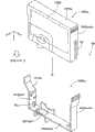
图30是表示第七实施例中的印刷装置1000K的说明图。与图1所示的印刷装置1000的区别在于:接受墨盒100K的固定器4K被固定在印刷装置1000K的框体上而不是包括印刷头的托架(未图示)。固定器4K和印刷头通过未图示的墨管连接。墨盒100K的墨水经由该管被供应给印刷头。 FIG. 30 is an explanatory diagram showing a
图31是墨盒100K的立体图。墨盒100K具有框体101K、电路基板200以及墨水供应口110K。框体101K包括前壁101Kwf以及底壁101Kwb。前壁101Kwf与底壁101Kwb交叉(在本实施例中实质上为正交)。在框体101K的内部收存有墨袋101P。 Fig. 31 is a perspective view of the
电路基板200与上述的各实施例的电路基板200相同。电路基板200被固定在框体101K的前壁101Kwf上。前壁101Kwf中的固定有电路基板200的部分的形状(例如突起P1、P2)与上述的实施例的前壁101wf相同(图6A)。 The
墨水供应口110K的结构与上述的各实施例的墨水供应口110的结构相同。墨水供应口110K被设置在框体101K的底壁101Kwb上。墨水供应口110K与墨袋101P连通。 The structure of the
在底壁101Kwb上还形成有定位孔127、128以及加压孔17。通过向加压孔17供应空气,可以向墨袋101P施加压力。为了促进墨水供应,而进行这样的加压。 Positioning holes 127 and 128 and a
图32是固定器4K的立体图。在本实施例中,固定器4K针对每个墨盒100K设置。固定器4K包括可动支承部102K、接点机构400K、供墨针6K、定位突出部103Ka、103Kb以及转动杆108K。可动支承部102K通过 与墨盒100K的底壁101Kwb(图31)接触,来支承墨盒100K。在可动支承部102K上固定有定位突出部103Ka、103Kb。定位突出部103Ka、103Kb在-Z方向上突出,并分别插入到墨盒100K的定位孔127、128中。在可动支承部102K的前方向(-Y方向)上固定有接点机构400K。该接点机构400K的结构与上述的接点机构400的结构相同(图11A和图11B)。虽然省略了图示,但是在各接点机构400K上连接有与托架电路500(图3)相同的电路。 FIG. 32 is a perspective view of the
在本实施例中,通过使墨盒100K在安装方向Z上移动,墨盒100K被安装在固定器4K上。这里,通过墨盒100K按压在可动支承部102K上,可动支承部102K在+Z方向上移动。图32中的第二个固定器4K(4Ka)表示了墨盒100K被安装前的状态。第三个固定器4K(4Kb)表示了墨盒100K被安装了的状态(省略了墨盒100K的图示)。以下,将通过固定器4Kb表示的可动支承部102K的位置也称为“安装位置”。通过可动支承部102K在+Z方向上移动,供墨针6K出现在可动支承部102K的-Z方向上。并且,供墨针6K被插入到墨盒100K的墨水供应口110K(图31)中。 In this embodiment, the
当安装墨盒100K时,墨盒100K(可动支承部102K)暂且被按压到比安装位置深的位置(向+Z方向偏移的位置)。由此,设置在转动杆108K的顶端的销112K与墨盒100K的未图示的卡定部卡合。并且,墨盒100K(可动支承部102K)被保持在安装位置。如果将墨盒100K(可动支承部102K)再次按压到比安装位置深的位置,则销112K的卡合被解除。然后,墨盒100K被从固定器4K中排出。作为这样的转动杆108K和卡定部的结构,可以采用已知的各种结构。 When the
在本实施例中,墨盒100K与第一实施例的墨盒100相同,可围绕墨水供应口110K摆动。因此,在本实施例中,也可产生与上述的第一实施例的墨盒100相同的各种不良情况。因此,在本实施例中,在墨盒100K上设置有与上述的墨盒100相同的电路基板200以及墨水供应口110K。电路基板200和墨水供应口110K的结构分别与第一实施例的电路基板200和墨水供应口110的结构相同。另外,电路基板200的第一线L1(图 10C)与其他的线相比,靠近墨水供应口110K的开口。即,墨盒100K具有与第一实施例的墨盒100相同的结构(例如,结构1~结构7)。结果,本实施例的墨盒100K具有与第一实施例的墨盒100相同的各种优点。 In this embodiment, the
I.电路基板的变形例: I. Variations of the circuit board:
图33是表示电路基板的其他实施例的说明图。与图10C所示的电路基板200的区别在于:七个端子210G~270G被配置成形成在X方向上延伸的一条线。各端子210G~270G与第一实施例的端子210~270相比,形成为在Z方向上长的近似矩形状。另外,端子210G~270G的接触部210Gc~270Gc的配置与第一实施例的接触部210c~270c的配置相同。因此,在上述的各实施例中,代替电路基板200、200d的端子210~270而采用该电路基板200G的端子210G~270G的情况也能够得到上述各种优点。 Fig. 33 is an explanatory view showing another example of a circuit board. The difference from the
图34是表示电路基板的其他实施例的说明图。与图10C所示的电路基板200的区别在于:各端子210H~270H的形状被不规则地确定。在该实施例中,端子210H~270H的接触部210Hc~270Hc的配置与第一实施例的接触部210c~270c的配置相同。因此,在上述的各实施例中,代替电路基板200、200d的端子210~270而采用该电路基板200H的端子210H~270H的情况也能够得到上述的各种优点。 Fig. 34 is an explanatory diagram showing another example of a circuit board. The difference from the
图35是表示电路基板的其他实施例的说明图。与图10C所示的电路基板200的区别在于:各端子210J~270J的形状被不规则地确定。另外,在该实施例的电路基板200J中,与上述的电路基板200、200G不同,当沿安装方向Z(从-Z向+Z)观察时,以多个端子重叠的方式来确定端子210J~270J的形状。在该实施例中,端子210J~270J的接触部210Jc~270Jc的配置与第一实施例的接触部210c~270c的配置相同。因此,在上述的各实施例中,代替电路基板200、200d的端子210~270而采用该电路基板200J的端子210J~270J的情况也能够得到上述的各种优点。 Fig. 35 is an explanatory view showing another example of a circuit board. The difference from the
图36是表示电路基板的其他实施例的说明图。五个端子210K~250K除了与图10C的端子210~250相同的导电部分以外,还包括向-Z方向延 伸的线状的导电部分。两个端子260K、270K除了与图10C的端子260、270相同的导电部分以外还包括向+Z方向延伸的线状的导电部分。在该实施例中,端子210K~270K的接触部210Kc~270Kc的配置与第一实施例的接触部210c~270c的配置相同。因此,在上述的各实施例中,代替电路基板200、200d的端子210~270而采用该电路基板200K的端子210K~270K的情况也能够得到上述的各种优点。 Fig. 36 is an explanatory diagram showing another example of a circuit board. The five
J.变形例: J. Variation:
另外,该发明不限于上述的实施例和实施方式,可以在不脱离其主旨的范围内在各种方式中实施,例如也可以进行如下的变形。 In addition, this invention is not limited to the said Example and embodiment, It can implement in various forms in the range which does not deviate from the summary, For example, the following deformation|transformation is also possible. the
变形例1: Variation 1:
在图21所示的实施例中,电源端子220的接触部220c也可以配置在与中心线CL重叠的位置上。另外,整个电路基板200也可以配置在不与中心线CL重叠的位置上。另外,也可以当沿安装方向Z(从-Z向+Z)观察时,配置成一部分的接触部与其他的接触部重叠。 In the embodiment shown in FIG. 21, the
无论哪种情况均优选电源端子的接触部配置在前头的线(第一线L1)上。这样一来,能够降低电源端子的连接不良的可能性,因此能够降低利用经由端子的电连接时的发生不良情况的可能性。 In either case, it is preferable that the contact portion of the power supply terminal is arranged on the leading line (first line L1 ). In this way, the possibility of poor connection of the power supply terminal can be reduced, and thus the possibility of occurrence of a failure when using electrical connection via the terminal can be reduced. the
变形例2: Modification 2:
在上述的各实施例中,作为墨盒100、100K和接合器100A、100Aa、100Ab、100Ac、100Ad所安装的设备,可以采用各种设备。例如传感器104也可以是对墨盒100内的墨水施加电压并测定其电阻值的传感器。可以根据电阻值来检测墨水的性质和状态、量。另外,作为用于墨盒100、100K和接合器100A、100Aa、100Ab、100Ac、100Ad的安装的检测的设备,不限于压电元件,可以采用各种设备。例如,也可以代替压电元件而采用电容器。另外,也可以采用连接(短路)两个端子的导电路径。当采用导电路径时,通过确认两个端子之间的导通,能够检测出安装。另外,也可以与检测墨水余量的传感器不同,而设置用于安装的检测的设备(在此情况下,增加了用于增加设备的端子)。另外,在上述的各实施例中,也可以省略检测墨水余量的传感器。 In each of the above-described embodiments, various devices can be used as devices to which the
另外,作为存储装置203的结构,不限于图15所示的结构,可以采用各种结构。例如,当存储装置203包括寄生二极管时,也可以省略形成与该寄生二极管同等的电路的保护二极管。另外,也可以将不基于时钟信号生成存储器地址而从外部装置(例如,图3的印刷装置1000的控制部(主控制电路40和托架电路500的整体))利用数据信号线来接收指令、存储器地址的串行存储器用作存储装置203。或者,也可以是印刷装置的控制部与多个存储装置分别连接,而不是多个存储装置通过总线连接与印刷装置的控制部连接。在此情况下,印刷装置的控制部也可以代替重置信号而将芯片选择信号发送给作为访问对象的存储装置,并通过芯片选择信号的电平来控制重置状态和动作状态。这样的存储器的动作(例如,存储器内部的计数、登记的值)根据芯片选择信号的变化而被重置。因此,芯片选择信号相当于“重置信号”。另外,也可以从上述实施例的存储装置中省略重置端子接点,而基于提供给电源接点的电源电位的电平的变化,来执行根据上述实施方式的存储装置的重置信号的电平变化由存储装置执行的动作。在此情况下,基于电源电位被提供,存储装置变为动作状态,电源电位的提供停止时,存储装置被重置。另外,不限于存储装置203,可以采用进行数据信号的发送和接收的至少一者的各种设备。例如,也可以采用数据的更新被禁止的存储器(例如,ROM)。这样的存储器也可以存储表示墨水种类的信息。另外,也可以采用具有CPU和存储器的嵌入式存储器。这样一来,能够进行与基于CPU的数据处理的算法相应的柔性控制。无论哪种情况,作为设备,均可以采用从记录材料消耗装置(例如,图3的印刷装置1000)接受电源电位而动作的各种设备。当利用接受电源电位的供应而动作的设备时,电源电位供应的切断可以引起重大的不良情况(例如,误动作)。因此,优选用于接受电源电位的接触部被配置在前头的线上。 In addition, the configuration of the
另外,作为设备的配置,可以采用任意的配置。例如,存储装置203(图3)也可以直接固定在与基板不同的其他的部件(例如,图6A、图6B的框体101、图22的主体101A或者图31的框体101K)上。 In addition, as the configuration of the device, any configuration can be adopted. For example, the storage device 203 ( FIG. 3 ) may also be directly fixed on other components (for example, the
另外,作为端子的总数,可以采用与被利用的设备相应的任意数量。 并且,也可以将多个接触部配置成形成三条以上的线。另外,前头线以外的线也可以包括接触部的总数比前头线多的线。无论哪种情况,如果将多个接触部分散地配置在多条线上,则如图21所示能够缩短各接触部与中心线CL的距离。结果,能够降低各接触部的位置偏差。 In addition, as the total number of terminals, any number corresponding to the devices to be used can be employed. Also, a plurality of contact portions may be arranged to form three or more lines. In addition, the lines other than the front line may include lines having a total number of contact portions greater than that of the front line. In any case, if a plurality of contact portions are dispersedly arranged on a plurality of lines, the distance between each contact portion and the center line CL can be shortened as shown in FIG. 21 . As a result, positional deviation of each contact portion can be reduced. the
变形例3: Variation 3:
在上述的各实施例中,作为墨水供应系统的结构,不限于图6A~图9、图22~图23、图25~图26、图27、图28、图29、图31所示的结构,可以采用各种结构。例如,也可以在一个墨盒上设置多个墨水容纳部(设置墨水室和墨水供应口)。 In each of the above-mentioned embodiments, the structure of the ink supply system is not limited to the structures shown in FIGS. 6A to 9, FIGS. , various structures can be adopted. For example, one ink cartridge may be provided with a plurality of ink storage portions (an ink chamber and an ink supply port are provided). the
另外,也可以将多个端子的至少一部分直接地形成在与基板不同的其他部件(例如,图6A、图6B的前壁101wf、图22的前壁101Awf、图31的前壁101Kwf)上。另外,不限于端子直接形成在前壁上的情况,端子形成在安装于前壁的基板上的情况也可以说是:“端子设置在前壁上”。 In addition, at least a part of the plurality of terminals may be directly formed on other components (for example, the front wall 101wf in FIGS. 6A and 6B , the front wall 101Awf in FIG. 22 , and the front wall 101Kwf in FIG. 31 ) different from the substrate. In addition, not limited to the case where the terminals are directly formed on the front wall, the case where the terminals are formed on a substrate mounted on the front wall can also be said to be "the terminals are provided on the front wall". the
另外,作为用于将与记录材料消耗装置(例如,图3的印刷装置000)电连接的电路基板安装(连接)在记录材料消耗装置上的结构,可以采用各种结构。例如,也可以如图6A和图31所示的实施例那样将电路基板固定在墨盒上。另外,也可以如图22~图29所示的实施例那样,将电路基板固定在构造体(接合器)上。这里,作为构造体(接合器)的结构,可以采用各种结构。例如,可以如图22~图27所示的实施例那样,采用单独安装在记录材料消耗装置上的结构。另外,也可以如图28、图29所示的实施例那样,在构造体被固定在记录材料容纳部(例如,图28的墨水容纳部100Ba)上的状态下,构造体与该记录材料容纳部一起安装在记录材料消耗装置上。无论哪种情况,当构造体的位置由记录材料容纳部确定(被限制)时、即构造体由于记录材料容纳部的运动而运动时,可以说构造体被记录材料容纳部支承。 In addition, as a structure for mounting (connecting) a circuit board electrically connected to a recording material consuming device (for example, the printing device 000 of FIG. 3 ) on the recording material consuming device, various structures can be adopted. For example, it is also possible to fix the circuit board on the ink cartridge as in the embodiment shown in Fig. 6A and Fig. 31 . In addition, the circuit board may be fixed to the structure (bonder) as in the embodiments shown in FIGS. 22 to 29 . Here, as the structure of the structure (adapter), various structures can be adopted. For example, as in the embodiments shown in FIGS. 22 to 27 , a structure in which the recording material consumption device is separately installed may be employed. In addition, like the embodiments shown in FIGS. 28 and 29 , the structure and the recording material may be accommodated in a state where the structure is fixed to the recording material container (for example, the ink container 100Ba in FIG. 28 ). together with the recording material consumption unit. In either case, when the position of the structure is determined (restricted) by the recording material accommodating portion, that is, when the structure moves due to the movement of the recording material accommodating portion, it can be said that the structure is supported by the recording material accommodating portion. the
变形例4: Variation 4:
印刷装置同时可利用的墨盒的总数不限于6,可以采用任意的数目(例如,1、4、8)。另外,可利用的墨水的种类也可以采用各个种类。例如,也可以采用比黑色墨水明快的灰色墨水。另外,也可以采用专色墨 水(例如,红色墨水或蓝色墨水)。另外,也可以采用不含着色剂的墨水(例如,包含保护墨点的成分的无色透明的墨水)。 The total number of ink cartridges available to the printing device at the same time is not limited to 6, and any number (for example, 1, 4, 8) can be used. In addition, various types of inks that can be used can also be used. For example, gray ink, which is brighter than black ink, may also be used. Alternatively, spot color inks (for example, red ink or blue ink) may be used. In addition, an ink that does not contain a colorant (for example, a colorless and transparent ink containing a component that protects ink dots) may also be used. the
另外,在上述的各实施例中,作为记录材料,不限于墨水,可以采用各种记录材料。例如,也可以采用调色剂。另外,作为记录材料消耗装置,不限于印刷装置,可以采用消耗记录材料的各种装置。 In addition, in each of the above-described embodiments, the recording material is not limited to ink, and various recording materials can be used. For example, toner may also be used. In addition, the recording material consumption device is not limited to a printing device, and various devices that consume recording materials can be employed. the
变形例5: Variation 5:
在上述的各实施例中,可以将通过硬件实现的结构的一部分置换成软件,相反地,也可以将通过软件实现的结构的一部分或全部置换成硬件。例如,也可以通过具有逻辑电路的硬件电路来实现图3的墨水余量检测模块M20的功能。 In each of the above-described embodiments, a part of the configuration realized by hardware may be replaced by software, and conversely, a part or all of the configuration realized by software may be replaced by hardware. For example, the function of the remaining ink amount detection module M20 in FIG. 3 may also be realized by a hardware circuit including a logic circuit. the
另外,当本发明的功能的一部分或全部通过软件来实现时,该软件(计算机程序)可以通过存储在计算机可读取的记录介质上的形式来提供。在该发明中,“计算机可读取的记录介质”不限于软盘或CD-ROM这样的携带型的记录介质,也可以包含各种RAM、ROM等计算机内的内部存储装置或者硬盘等固定在计算机上的外部存储装置。 In addition, when a part or all of the functions of the present invention are realized by software, the software (computer program) can be provided in a form stored on a computer-readable recording medium. In this invention, the "computer-readable recording medium" is not limited to portable recording media such as floppy disks and CD-ROMs, and may also include internal storage devices such as various RAMs and ROMs in computers, or hard disks, etc. fixed in computers. on the external storage device. the
Claims (26)
Translated fromChineseApplications Claiming Priority (2)
| Application Number | Priority Date | Filing Date | Title |
|---|---|---|---|
| JP2009-118175 | 2009-05-15 | ||
| JP2009118175 | 2009-05-15 |
Publications (1)
| Publication Number | Publication Date |
|---|---|
| CN202053682Utrue CN202053682U (en) | 2011-11-30 |
Family
ID=42629336
Family Applications (3)
| Application Number | Title | Priority Date | Filing Date |
|---|---|---|---|
| CN201080002628.5AActiveCN102159402B (en) | 2009-05-15 | 2010-05-14 | Recording material supply system, circuit board, structure, and ink cartridge |
| CN2010201988260UExpired - Fee RelatedCN202053682U (en) | 2009-05-15 | 2010-05-14 | Recording material supply system, circuit board, construction body and cartridge |
| CN201410131137.0AActiveCN103950293B (en) | 2009-05-15 | 2010-05-14 | Recording materials supply system, circuit substrate, tectosome and print cartridge |
Family Applications Before (1)
| Application Number | Title | Priority Date | Filing Date |
|---|---|---|---|
| CN201080002628.5AActiveCN102159402B (en) | 2009-05-15 | 2010-05-14 | Recording material supply system, circuit board, structure, and ink cartridge |
Family Applications After (1)
| Application Number | Title | Priority Date | Filing Date |
|---|---|---|---|
| CN201410131137.0AActiveCN103950293B (en) | 2009-05-15 | 2010-05-14 | Recording materials supply system, circuit substrate, tectosome and print cartridge |
Country Status (28)
| Country | Link |
|---|---|
| US (2) | US8540347B2 (en) |
| EP (4) | EP2730417B2 (en) |
| JP (3) | JP5321683B2 (en) |
| KR (1) | KR101692564B1 (en) |
| CN (3) | CN102159402B (en) |
| AU (1) | AU2010248649B2 (en) |
| BR (1) | BRPI1004348A2 (en) |
| CA (1) | CA2735829C (en) |
| CL (2) | CL2011000457A1 (en) |
| CO (1) | CO6361968A2 (en) |
| DE (2) | DE112010002008T5 (en) |
| EG (1) | EG26262A (en) |
| ES (3) | ES2531908T5 (en) |
| GB (1) | GB2482214A (en) |
| IL (2) | IL211455A (en) |
| IT (1) | ITTO20100090U1 (en) |
| MA (1) | MA32605B1 (en) |
| MX (1) | MX2011002371A (en) |
| MY (2) | MY168499A (en) |
| NZ (1) | NZ591273A (en) |
| PE (1) | PE20110372A1 (en) |
| PL (3) | PL2730417T5 (en) |
| PT (3) | PT2730417E (en) |
| RU (3) | RU2535284C2 (en) |
| SG (1) | SG10201401997XA (en) |
| UA (1) | UA105184C2 (en) |
| WO (1) | WO2010131480A1 (en) |
| ZA (1) | ZA201101411B (en) |
Cited By (2)
| Publication number | Priority date | Publication date | Assignee | Title |
|---|---|---|---|---|
| CN104723687A (en)* | 2013-12-18 | 2015-06-24 | 精工爱普生株式会社 | Liquid Supply Unit |
| CN109605941A (en)* | 2019-01-30 | 2019-04-12 | 北海绩迅电子科技有限公司 | A kind of liner print cartridge and its processing method |
Families Citing this family (45)
| Publication number | Priority date | Publication date | Assignee | Title |
|---|---|---|---|---|
| JP4144637B2 (en)* | 2005-12-26 | 2008-09-03 | セイコーエプソン株式会社 | Printing material container, substrate, printing apparatus, and method for preparing printing material container |
| JP2010012602A (en)* | 2008-06-30 | 2010-01-21 | Brother Ind Ltd | Package and ink cartridge |
| CN102161279B (en)* | 2008-06-30 | 2013-10-16 | 兄弟工业株式会社 | Adaptor for ink cartridge |
| KR100986744B1 (en)* | 2008-07-10 | 2010-10-08 | 주식회사 한랩 | Automatic Balancing Centrifuge and its Control Method |
| US8540347B2 (en) | 2009-05-15 | 2013-09-24 | Seiko Epson Corporation | Recording material delivery system for recording material-consuming apparatus; circuit board; structural body; and ink cartridge |
| CN102233737B (en)* | 2010-05-01 | 2015-04-08 | 珠海纳思达企业管理有限公司 | Cartridges, cartridge sets, and cartridge identification systems |
| US8764172B2 (en) | 2010-09-03 | 2014-07-01 | Seiko Epson Corporation | Printing apparatus, printing material cartridge, adaptor for printing material container, and circuit board |
| JP5750849B2 (en)* | 2010-09-03 | 2015-07-22 | セイコーエプソン株式会社 | Printing device, cartridge set, and adapter set |
| JP5776385B2 (en) | 2010-09-03 | 2015-09-09 | セイコーエプソン株式会社 | Printing device |
| JP5720148B2 (en) | 2010-09-03 | 2015-05-20 | セイコーエプソン株式会社 | Printing material cartridge and printing material supply system |
| ITUD20100237A1 (en)* | 2010-12-29 | 2012-06-30 | Nicolas Simonin | ADAPTER DEVICE FOR A CARTRIDGE OF A PRINTER EQUIPMENT |
| JP5765027B2 (en)* | 2011-04-08 | 2015-08-19 | セイコーエプソン株式会社 | RECORDING DEVICE AND TERMINAL MODULE FOR RECORDING DEVICE |
| JP5853436B2 (en)* | 2011-06-23 | 2016-02-09 | セイコーエプソン株式会社 | Printing device |
| US8801161B2 (en) | 2011-07-27 | 2014-08-12 | Brother Kogyo Kabushiki Kaisha | Liquid cartridge, image recording device, and substrate |
| DE102011052211B8 (en)* | 2011-07-27 | 2025-07-31 | Brother Kogyo Kabushiki Kaisha | Liquid container and image recording device |
| EP2738005B1 (en)* | 2011-07-28 | 2018-02-21 | Brother Kogyo Kabushiki Kaisha | Liquid cartridge and liquid ejection device |
| JP5915094B2 (en)* | 2011-11-04 | 2016-05-11 | セイコーエプソン株式会社 | Printing device |
| CN202428832U (en) | 2012-01-13 | 2012-09-12 | 珠海并洲贸易有限公司 | Chip for printer and ink box comprising same |
| JP5962144B2 (en)* | 2012-03-30 | 2016-08-03 | ブラザー工業株式会社 | Printing fluid storage device and printing fluid supply device |
| JP2013248779A (en)* | 2012-05-31 | 2013-12-12 | Seiko Epson Corp | Ink cartridge and printer |
| JP6354117B2 (en)* | 2012-08-31 | 2018-07-11 | セイコーエプソン株式会社 | Holding member and liquid container |
| JP6375609B2 (en)* | 2012-10-19 | 2018-08-22 | 株式会社リコー | Detachable device and image forming apparatus |
| KR101326098B1 (en)* | 2013-01-21 | 2013-11-06 | 주식회사 아이비에스 | Method for inspecting wire bonding |
| JP6142571B2 (en)* | 2013-02-28 | 2017-06-07 | セイコーエプソン株式会社 | Cartridge, liquid supply system, liquid ejection device |
| DE202013006492U1 (en) | 2013-07-19 | 2013-08-21 | Artech Gmbh Design + Production In Plastic | Control module for mounting on a consumable cartridge and ink cartridge for a printer |
| DE202013007283U1 (en)* | 2013-08-14 | 2013-09-25 | Artech Gmbh Design + Production In Plastic | Integrated electronic circuit for a control module for mounting on a consumable cartridge, control module and consumable cartridge for a printer |
| KR102002888B1 (en)* | 2013-11-05 | 2019-07-23 | 휴렛-팩커드 디벨롭먼트 컴퍼니, 엘.피. | Electronic device and method for checking connected state of signal line thereof |
| TWI556984B (en)* | 2014-09-05 | 2016-11-11 | 研能科技股份有限公司 | Flexible interconnect circuit for using in printing cartridge |
| JP6586754B2 (en)* | 2015-03-20 | 2019-10-09 | セイコーエプソン株式会社 | Liquid consumption device |
| CN104842662B (en)* | 2015-05-22 | 2017-01-04 | 杭州旗捷科技有限公司 | Printing device, printed material container and chip thereof, the above two electric connection structure |
| CN108430784B (en)* | 2015-12-28 | 2020-06-23 | 精工爱普生株式会社 | liquid supply unit |
| WO2017115582A1 (en)* | 2015-12-28 | 2017-07-06 | セイコーエプソン株式会社 | Liquid supply unit |
| JP6651846B2 (en)* | 2015-12-28 | 2020-02-19 | セイコーエプソン株式会社 | Liquid supply unit, liquid ejection system |
| CN105549361A (en)* | 2015-12-31 | 2016-05-04 | 珠海奔图电子有限公司 | Storage element, developing cartridge using same, and image forming apparatus |
| CN106527081B (en)* | 2016-08-10 | 2023-06-06 | 江西亿铂电子科技有限公司 | Developing box |
| CN107718888B (en)* | 2016-08-12 | 2019-10-18 | 珠海纳思达企业管理有限公司 | Print cartridge and ink-jet printer |
| JP2018062064A (en)* | 2016-10-11 | 2018-04-19 | セイコーエプソン株式会社 | Liquid supply unit |
| CN107187203A (en)* | 2017-07-05 | 2017-09-22 | 苏州锟恩电子科技有限公司 | A kind of self-cleaning inkjet printing header structure |
| CN113710496A (en)* | 2019-04-29 | 2021-11-26 | 惠普发展公司, 有限责任合伙企业 | Rotary housing with sensor |
| KR20220005301A (en) | 2020-07-06 | 2022-01-13 | 휴렛-팩커드 디벨롭먼트 컴퍼니, 엘.피. | structure for driving toner inlet shutter of developing cartridge by using motor |
| KR102497612B1 (en) | 2020-07-23 | 2023-02-07 | 백영기 | Ink supplying device |
| JP7552208B2 (en)* | 2020-09-30 | 2024-09-18 | 京セラドキュメントソリューションズ株式会社 | Developing device and image forming apparatus |
| CN112743991B (en)* | 2021-01-26 | 2021-12-17 | 北海绩迅电子科技有限公司 | ink cartridge |
| JP7605663B2 (en)* | 2021-03-10 | 2024-12-24 | 株式会社キーエンス | Inkjet recording device and intermediate connector applied thereto |
| US11535038B1 (en)* | 2021-12-28 | 2022-12-27 | Seiko Epson Corporation | Board, liquid accommodation container, and printing system |
Family Cites Families (20)
| Publication number | Priority date | Publication date | Assignee | Title |
|---|---|---|---|---|
| JP3222454B2 (en)* | 1990-02-02 | 2001-10-29 | キヤノン株式会社 | Ink tank cartridge |
| AU3241795A (en)* | 1994-08-09 | 1996-03-07 | Encad, Inc. | Printer ink cartridge |
| JPH10230603A (en) | 1997-02-19 | 1998-09-02 | Canon Inc | Ink jet recording head, method of assembling the same, and ink jet recording apparatus using the head |
| EP2179848A1 (en)* | 1998-05-18 | 2010-04-28 | Seiko Epson Corporation | Ink-jet printing apparatus and ink cartridge therefor |
| JP3945015B2 (en) | 1998-05-19 | 2007-07-18 | ブラザー工業株式会社 | Contact structure of ink jet recording apparatus |
| JP3649123B2 (en)† | 2000-12-26 | 2005-05-18 | セイコーエプソン株式会社 | Circuit board terminals |
| JP4469686B2 (en) | 2003-08-29 | 2010-05-26 | セイコーエプソン株式会社 | Liquid ejector |
| JP4338202B2 (en) | 2004-06-02 | 2009-10-07 | キヤノン株式会社 | Liquid discharge head and liquid discharge apparatus including the same |
| WO2006025578A1 (en) | 2004-09-01 | 2006-03-09 | Seiko Epson Corporation | Printing material housing device |
| RU2412058C1 (en)* | 2005-03-28 | 2011-02-20 | Сейко Эпсон Корпорейшн | Cartridge with liquid, device to load-unload cartridge with liquid, printing device and device for liquid ejection |
| JP4144637B2 (en)* | 2005-12-26 | 2008-09-03 | セイコーエプソン株式会社 | Printing material container, substrate, printing apparatus, and method for preparing printing material container |
| JP4341688B2 (en)* | 2006-04-12 | 2009-10-07 | セイコーエプソン株式会社 | Liquid container |
| JP4232793B2 (en)* | 2006-05-31 | 2009-03-04 | セイコーエプソン株式会社 | Liquid consumption apparatus and liquid consumption management method |
| US8267495B2 (en) | 2006-12-26 | 2012-09-18 | Seiko Epson Corporation | Liquid container with residual liquid quantity detecting unit and method of manufacturing the same |
| JP2008221569A (en)* | 2007-03-12 | 2008-09-25 | Seiko Epson Corp | Printing recording material container |
| US7758138B2 (en)* | 2007-10-01 | 2010-07-20 | Seiko Epson Corporation | Liquid jetting apparatus and control method configured to reduce effects of electrical fluctuations |
| JP5151841B2 (en)* | 2007-10-01 | 2013-02-27 | セイコーエプソン株式会社 | Liquid ejecting apparatus and method for controlling liquid ejecting apparatus |
| JP2009118175A (en) | 2007-11-06 | 2009-05-28 | Japan Radio Co Ltd | Receiver |
| JP2010111116A (en)* | 2008-10-09 | 2010-05-20 | Seiko Epson Corp | Circuit board and liquid supplying unit |
| US8540347B2 (en) | 2009-05-15 | 2013-09-24 | Seiko Epson Corporation | Recording material delivery system for recording material-consuming apparatus; circuit board; structural body; and ink cartridge |
- 2010
- 2010-05-13USUS12/779,511patent/US8540347B2/enactiveActive
- 2010-05-14RURU2011106323/12Apatent/RU2535284C2/enactive
- 2010-05-14CNCN201080002628.5Apatent/CN102159402B/enactiveActive
- 2010-05-14ESES14150287Tpatent/ES2531908T5/enactiveActive
- 2010-05-14CACA2735829Apatent/CA2735829C/ennot_activeExpired - Fee Related
- 2010-05-14DEDE112010002008Tpatent/DE112010002008T5/ennot_activeWithdrawn
- 2010-05-14MYMYPI2014001709Apatent/MY168499A/enunknown
- 2010-05-14PLPL14150287Tpatent/PL2730417T5/enunknown
- 2010-05-14ESES10774739.6Tpatent/ES2436842T3/enactiveActive
- 2010-05-14SGSG10201401997XApatent/SG10201401997XA/enunknown
- 2010-05-14GBGB1103581.3Apatent/GB2482214A/ennot_activeWithdrawn
- 2010-05-14MYMYPI2011000901Apatent/MY155500A/enunknown
- 2010-05-14BRBRPI1004348Apatent/BRPI1004348A2/ennot_activeApplication Discontinuation
- 2010-05-14KRKR1020117005004Apatent/KR101692564B1/ennot_activeExpired - Fee Related
- 2010-05-14PTPT141502872Tpatent/PT2730417E/enunknown
- 2010-05-14NZNZ591273Apatent/NZ591273A/ennot_activeIP Right Cessation
- 2010-05-14WOPCT/JP2010/003271patent/WO2010131480A1/enactiveApplication Filing
- 2010-05-14EPEP14150287.2Apatent/EP2730417B2/ennot_activeNot-in-force
- 2010-05-14DEDE202010006814Upatent/DE202010006814U1/ennot_activeExpired - Lifetime
- 2010-05-14CNCN2010201988260Upatent/CN202053682U/ennot_activeExpired - Fee Related
- 2010-05-14EPEP13163418.0Apatent/EP2614961B2/ennot_activeNot-in-force
- 2010-05-14AUAU2010248649Apatent/AU2010248649B2/ennot_activeCeased
- 2010-05-14UAUAA201102591Apatent/UA105184C2/enunknown
- 2010-05-14CNCN201410131137.0Apatent/CN103950293B/enactiveActive
- 2010-05-14JPJP2011513253Apatent/JP5321683B2/enactiveActive
- 2010-05-14PLPL13163418Tpatent/PL2614961T5/enunknown
- 2010-05-14ESES13163418.0Tpatent/ES2528918T5/enactiveActive
- 2010-05-14EPEP10774739.6Apatent/EP2316656B1/enactiveActive
- 2010-05-14MXMX2011002371Apatent/MX2011002371A/enactiveIP Right Grant
- 2010-05-14PTPT131634180Tpatent/PT2614961E/enunknown
- 2010-05-14RURU2010119517/12Upatent/RU101405U1/ennot_activeIP Right Cessation
- 2010-05-14PEPE2011000195Apatent/PE20110372A1/ennot_activeApplication Discontinuation
- 2010-05-14PLPL10774739Tpatent/PL2316656T3/enunknown
- 2010-05-14EPEP14150291.4Apatent/EP2719538A1/ennot_activeWithdrawn
- 2010-05-14PTPT107747396Tpatent/PT2316656E/enunknown
- 2010-05-14ITIT000090Upatent/ITTO20100090U1/enunknown
- 2011
- 2011-02-22EGEG2011020287Apatent/EG26262A/enactive
- 2011-02-22ZAZA2011/01411Apatent/ZA201101411B/enunknown
- 2011-02-28ILIL211455Apatent/IL211455A/enactiveIP Right Grant
- 2011-03-01MAMA33662Apatent/MA32605B1/enunknown
- 2011-03-02CLCL2011000457Apatent/CL2011000457A1/enunknown
- 2011-03-04COCO11027125Apatent/CO6361968A2/enactiveIP Right Grant
- 2013
- 2013-04-08CLCL2013000945Apatent/CL2013000945A1/enunknown
- 2013-07-18JPJP2013149363Apatent/JP5867461B2/enactiveActive
- 2013-07-26USUS13/952,047patent/US9061508B2/enactiveActive
- 2013-12-26JPJP2013268700Apatent/JP5867497B2/enactiveActive
- 2014
- 2014-09-18RURU2014137896Apatent/RU2014137896A/ennot_activeApplication Discontinuation
- 2015
- 2015-04-30ILIL238542Apatent/IL238542A/enactiveIP Right Grant
Cited By (3)
| Publication number | Priority date | Publication date | Assignee | Title |
|---|---|---|---|---|
| CN104723687A (en)* | 2013-12-18 | 2015-06-24 | 精工爱普生株式会社 | Liquid Supply Unit |
| CN109605941A (en)* | 2019-01-30 | 2019-04-12 | 北海绩迅电子科技有限公司 | A kind of liner print cartridge and its processing method |
| CN109605941B (en)* | 2019-01-30 | 2020-03-10 | 北海绩迅电子科技有限公司 | Inner container ink box and processing method thereof |
Also Published As
Similar Documents
| Publication | Publication Date | Title |
|---|---|---|
| CN202053682U (en) | Recording material supply system, circuit board, construction body and cartridge | |
| AU2014202105B2 (en) | Recording material supply system, circuit board, structure, and ink cartridge for recording material consumption device | |
| CA2768790C (en) | Printing apparatus, printing material cartridge, adaptor for printing material container, and circuit board | |
| JP5630157B2 (en) | Printing device | |
| HK1196801B (en) | Recording material supply system, circuit board, structure, and ink cartridge for recording material consumption device |
Legal Events
| Date | Code | Title | Description |
|---|---|---|---|
| C14 | Grant of patent or utility model | ||
| GR01 | Patent grant | ||
| CF01 | Termination of patent right due to non-payment of annual fee | Granted publication date:20111130 Termination date:20190514 | |
| CF01 | Termination of patent right due to non-payment of annual fee |