CN201993738U - Projected capacitive touch panel - Google Patents
Projected capacitive touch panelDownload PDFInfo
- Publication number
- CN201993738U CN201993738UCN2011200684741UCN201120068474UCN201993738UCN 201993738 UCN201993738 UCN 201993738UCN 2011200684741 UCN2011200684741 UCN 2011200684741UCN 201120068474 UCN201120068474 UCN 201120068474UCN 201993738 UCN201993738 UCN 201993738U
- Authority
- CN
- China
- Prior art keywords
- axis
- inductive layer
- induction
- electrode
- sensing
- Prior art date
- Legal status (The legal status is an assumption and is not a legal conclusion. Google has not performed a legal analysis and makes no representation as to the accuracy of the status listed.)
- Expired - Fee Related
Links
- 230000006698inductionEffects0.000claimsabstract16
- 230000001939inductive effectEffects0.000claims16
- 239000003990capacitorSubstances0.000claims11
- 239000000463materialSubstances0.000claims3
- 229910003460diamondInorganic materials0.000claims1
- 239000010432diamondSubstances0.000claims1
- 230000035945sensitivityEffects0.000abstractdescription4
- 239000000758substrateSubstances0.000description13
- 238000012986modificationMethods0.000description2
- 230000004048modificationEffects0.000description2
- QNRATNLHPGXHMA-XZHTYLCXSA-N(r)-(6-ethoxyquinolin-4-yl)-[(2s,4s,5r)-5-ethyl-1-azabicyclo[2.2.2]octan-2-yl]methanol;hydrochlorideChemical compoundCl.C([C@H]([C@H](C1)CC)C2)CN1[C@@H]2[C@H](O)C1=CC=NC2=CC=C(OCC)C=C21QNRATNLHPGXHMA-XZHTYLCXSA-N0.000description1
- 238000000034methodMethods0.000description1
Images


Landscapes
- Fixed Capacitors And Capacitor Manufacturing Machines (AREA)
Abstract
Description
Translated fromChinese技术领域technical field
本实用新型是关于一种投射式电容触控面板,尤指一种可有效降低感应层上各电极内阻值的触控面板。The utility model relates to a projected capacitive touch panel, in particular to a touch panel which can effectively reduce the internal resistance of each electrode on the sensing layer.
背景技术Background technique
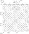
一种已知投射式电容触控面板的基本结构是如图4所示,其包括有:A basic structure of a known projected capacitive touch panel is shown in Figure 4, which includes:
一基板70,是呈透明状;A substrate 70 is transparent;
一X轴感应层80,是位于基板70上层,该X轴感应层80包括多数作横列排列的感应列,每一感应列是由多数呈菱形的X轴电极81相互连接所组成,又每一感应列分别与一X轴驱动线82连接;An
一Y轴感应层90,是位于基板70下层,该Y轴感应层90包括多数作直行排列的感应行,每一感应行是由多数呈菱形的Y轴电极91相互连接而成,又每一感应行分别与一Y轴驱动线92连接;A Y-
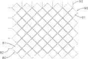
前述Y轴感应层90上的各个Y轴电极91是和X轴感应层80上各个X轴电极81相间或相对(对正),若各Y轴电极91与各X轴电极81的位置是相间排列(如图5所示),该投射式电容触控面板为一自容(Self Capacitance)型;若各Y轴电极91与各X轴电极81的位置是相互重迭,则该投射式电容触控面板为一互容(Mutual Capacitance)型。Each of the Y-
又前述X、Y轴感应层80,90上的X,Y轴驱动线82,92是分别与控制器连接,以便由控制器检测X,Y轴感应层80,90上各电容节点的电容值变化。由于投射式电容触控面板对于感应介面(X、Y轴感应层80,90)与控制器间的配合要求甚高,即使是相互垂直的X、Y轴驱动线82,92都必须考量其阻抗大小及内阻值均匀与否的问题,主要是因X、Y轴驱动线82,92的内阻值及均匀与否将直接影响触控面板输出的讯号杂讯比(S/N)。Also the aforementioned X and Y-
由上述可知,X、Y轴驱动线82,92是分别集中在X、Y轴感应层80,90上的一边上,供与控制器连接,在此状况下,各X、Y轴驱动线82,92与控制器的距离长度不可能相同,且存在相当差距,也就是X、Y轴驱动线82,92各自长短不一,而X、Y轴驱动线82,92的阻抗大小适与其长度适成正比,当面板尺寸愈大,驱动线愈长,其线阻抗即相对愈大,因而影响控制器判读的灵敏度,从而可能造成判读上的误差。As can be seen from the above, the X and Y
故由上述可知,既有投射式电容触控面板仍存在上述技术瓶颈,犹待进一步检讨并谋求可行的解决方案。Therefore, it can be seen from the above that the existing projected capacitive touch panel still has the above-mentioned technical bottlenecks, which need to be further reviewed and found a feasible solution.
实用新型内容Utility model content
因此本实用新型主要目的在提供一种投射式电容触控面板,其可有效降低感应层上的电极串内阻值,以提升控制器判读电容值变化的灵敏度。Therefore, the main purpose of the present invention is to provide a projected capacitive touch panel, which can effectively reduce the internal resistance of the electrode strings on the sensing layer, so as to improve the sensitivity of the controller to judge the change of capacitance.
为达成前述目的采用的主要技术手段是令前述投射式电容触控面板包括:The main technical means adopted to achieve the above-mentioned purpose is to make the above-mentioned projected capacitive touch panel include:
一X轴感应层,包括多数感应列,每一感应列的一端分设有一X轴驱动线,又每一感应列分别由两个以上并联的X轴电极串组成,每一X轴电极串是由多数的X轴电极相串组成;An X-axis sensing layer, including a plurality of sensing columns, one end of each sensing column is provided with an X-axis driving line, and each sensing column is composed of more than two parallel X-axis electrode strings, and each X-axis electrode string is composed of Most of the X-axis electrodes are connected in series;
一Y轴感应层,包括多数感应行,每一感应行的一端分设有一Y轴驱动线,又每一感应行分别由两个以上并联的Y轴电极串组成,每一Y轴电极串是由多数的Y轴电极相串组成;A Y-axis sensing layer, including a plurality of sensing rows, one end of each sensing row is provided with a Y-axis driving line, and each sensing row is composed of two or more Y-axis electrode strings connected in parallel, and each Y-axis electrode string is composed of Most of the Y-axis electrodes are connected in series;
由于本实用新型是令X、Y轴感应层上的感应列及感应行分别由两个以上并联的电极串组成,而两电极串在并联状况下将使内阻值变小,从而达成降低电极串内阻值的目的。Because the utility model makes the sensing columns and sensing rows on the X-axis and Y-axis sensing layers respectively composed of more than two parallel electrode strings, and the parallel connection of the two electrode strings will make the internal resistance smaller, thereby reducing the electrode The purpose of the internal resistance value of the string.
附图说明Description of drawings
图1是本实用新型一较佳实施例的立体角度示意图。Fig. 1 is a perspective view of a preferred embodiment of the utility model.
图2A是本实用新型一较佳实施例的X轴感应层平面示意图。FIG. 2A is a schematic plan view of an X-axis sensing layer in a preferred embodiment of the present invention.
图2B是本实用新型一较佳实施例的Y轴感应层平面示意图。2B is a schematic plan view of a Y-axis sensing layer in a preferred embodiment of the present invention.
图3是本实用新型一较佳实施例中X、Y轴感应层重迭后的平面示意图。Fig. 3 is a schematic plan view of overlapping X-axis and Y-axis sensing layers in a preferred embodiment of the present invention.
图4是既有投射式电容触控面板的立体角度示意图。FIG. 4 is a schematic perspective view of a conventional projected capacitive touch panel.
图5是既有投射式电容触控面板的平面示意图。FIG. 5 is a schematic plan view of a conventional projected capacitive touch panel.
具体实施方式Detailed ways
以下配合图式及本实用新型的较佳实施例,进一步阐述本实用新型为达成预定实用新型目的所采取的技术手段。In the following, in conjunction with the drawings and preferred embodiments of the utility model, the technical means adopted by the utility model to achieve the intended purpose of the utility model are further described.
关于本实用新型的第一较佳实施例,首先请参考图1所示,本实用新型的投射式电容触控面板包括:Regarding the first preferred embodiment of the present utility model, first please refer to FIG. 1, the projected capacitive touch panel of the present utility model includes:
一X轴感应层XS,请配合图2A所示,其包括多数感应列10,每一感应列10的一端分设有一X轴驱动线13,又每一感应列10分别由两个以上并联的X轴电极串11,12组成,本实施例中,每一感应列10分别由两并联的X轴电极串11,12组成,每一X轴电极串11,12是由多数的X轴电极111,121相串组成;An X-axis sensing layer XS, as shown in FIG. 2A, includes a plurality of
一Y轴感应层YS,请配合图2B所示,其包括多数感应行20,每一感应行20的一端分设有一Y轴驱动线23,又每一感应行20分别由两个以上并联的Y轴电极串21,22组成,本实施例中,每一感应行20分别由两并联的Y轴电极串21,22组成,每一Y轴电极串21,22是由多数的Y轴电极211,221相串组成;A Y-axis sensing layer YS, as shown in FIG. 2B, includes a plurality of
前述X轴感应层XS及Y轴感应层YS可以同时形成在一基材的同一表面上,且该X轴感应层XS的各个X轴电极111,121与Y轴感应层YS的各个Y轴电极211,221的位置是作相间排列(请参考图3所示),藉此构成一自容(Self Capacitance)型的投射式电容触控面板;请参考图1所示,于本实施例中,该X轴感应层XS、Y轴感应层YS是分别形成在两相对的基材30,40上;且其X轴电极111,121与Y轴电极211,221除位于两端者为三角形者,其余皆呈菱形。除上述形式,该X轴感应层XS及Y轴感应层YS可分别形成有一基材上相对的表底面,也可以分别形成有两基材的相对面上,而分别构成不同形式的自容型投射式电容触控面板。The aforementioned X-axis sensing layer XS and Y-axis sensing layer YS can be formed on the same surface of a substrate at the same time, and each
除前述自容型外,本实用新型也适用在互容型的投射式电容触控面板上,其一种可行实施例在于令前述X轴感应层XS形成在一基材的表面,而Y轴感应层YS则形成在同一基材的相对底面上,且Y轴感应层YS上各Y轴电极211,221的位置是与基材表面所设各X轴电极111,121重迭,而构成一互容(Mutual Capacitance)型投射式电容触控面板。又前述X轴感应层XS、Y轴感应层YS也可以分别形成在两基材的相对面上,而构成另一种不同态样的自容型投射式电容触控面板。该等X轴电极111,121与Y轴电极211,221除前述的三角形、菱形外,也可以为矩形。In addition to the aforementioned self-capacitance type, the utility model is also applicable to a mutual-capacitance type projected capacitive touch panel, and a possible embodiment thereof is to form the aforementioned X-axis sensing layer XS on the surface of a substrate, and the Y-axis The sensing layer YS is formed on the opposite bottom surface of the same substrate, and the positions of the Y-
再者,前述X轴感应层XS上每一感应列10的两X轴电极串11,12是相互并联,由于该等X轴电极串11,12由透明电极(ITO)构成而存在内阻,根据电阻公式,两电阻并联的阻值将小于两电阻各自原先的阻值(若两电阻的阻值不同,并联后阻值尚小于较低阻值电阻的阻值),换言之,当将两X轴电极串11,12并联后,该感应列10的阻值将会降低;同理,前述Y轴感应层YS上每一感应行20的两Y轴电极串21,22也是相互并联,因此感应行20的阻值也会降低,藉此可以提高控制器判读的灵敏度。Furthermore, the two
又如前揭所述,前述X轴感应层XS及Y轴感应层YS无论是形成在同一基材的表面、两面或分别形成在两基材的相对面上,必须进一步形成连接各感应列10、各感应行20的X,Y轴驱动线13,23,当面板尺寸愈大,愈接近面板边缘的感应列10、感应行20其X,Y轴驱动线13,23的长度愈长,与控制器连接埠的距离愈远,相对的线阻抗即愈大,同时也使各感应列10间与各感应行20间的内阻值不均,从而影响控制器判读的准确性,而上述问题也就是目前投射式电容触控面板尺寸无法加大的主要原因之一。As mentioned above, no matter whether the aforementioned X-axis sensing layer XS and Y-axis sensing layer YS are formed on the surface, both sides of the same substrate, or respectively formed on opposite surfaces of the two substrates, it is necessary to further form and connect the
而利用本实用新型的技术可有效降低各感应列10、各感应行20的内阻值,从而可降低各感应列10、各感应行20到控制器的整体线阻抗,故可相对提高控制器判读的准确性。And utilizing the technology of the present utility model can effectively reduce the internal resistance value of each
以上所述仅是本实用新型的较佳实施例而已,并非对本实用新型做任何形式上的限制,虽然本实用新型已以较佳实施例揭露如上,然而并非用以限定本实用新型,任何熟悉本专业的技术人员,在不脱离本实用新型技术方案的范围内,当可利用上述揭示的技术内容作出些许更动或修饰为等同变化的等效实施例,但凡是未脱离本实用新型技术方案的内容,依据本实用新型的技术实质对以上实施例所作的任何简单修改、等同变化与修饰,均仍属于本实用新型技术方案的范围内。The above descriptions are only preferred embodiments of the utility model, and do not limit the utility model in any form. Although the utility model has been disclosed as above with preferred embodiments, it is not used to limit the utility model. Those skilled in the art, without departing from the scope of the technical solution of the utility model, can use the technical content disclosed above to make some changes or modify equivalent embodiments with equivalent changes, but all the technical solutions of the utility model do not depart from Any simple modifications, equivalent changes and modifications made to the above embodiments according to the technical essence of the utility model still belong to the scope of the technical solution of the utility model.
Claims (8)
Priority Applications (1)
| Application Number | Priority Date | Filing Date | Title |
|---|---|---|---|
| CN2011200684741UCN201993738U (en) | 2011-03-15 | 2011-03-15 | Projected capacitive touch panel |
Applications Claiming Priority (1)
| Application Number | Priority Date | Filing Date | Title |
|---|---|---|---|
| CN2011200684741UCN201993738U (en) | 2011-03-15 | 2011-03-15 | Projected capacitive touch panel |
Publications (1)
| Publication Number | Publication Date |
|---|---|
| CN201993738Utrue CN201993738U (en) | 2011-09-28 |
Family
ID=44670221
Family Applications (1)
| Application Number | Title | Priority Date | Filing Date |
|---|---|---|---|
| CN2011200684741UExpired - Fee RelatedCN201993738U (en) | 2011-03-15 | 2011-03-15 | Projected capacitive touch panel |
Country Status (1)
| Country | Link |
|---|---|
| CN (1) | CN201993738U (en) |
Cited By (4)
| Publication number | Priority date | Publication date | Assignee | Title |
|---|---|---|---|---|
| CN103698949A (en)* | 2013-12-27 | 2014-04-02 | 合肥京东方光电科技有限公司 | Array substrate, display device and driving method thereof |
| CN103713412A (en)* | 2012-10-08 | 2014-04-09 | 群康科技(深圳)有限公司 | Touch display equipment and driving method thereof |
| TWI448941B (en)* | 2012-05-22 | 2014-08-11 | Hongkong Dongshan Prec Union Opoelectronic Co Ltd | Single side multi - touch panel and its manufacturing method |
| WO2017097205A1 (en)* | 2015-12-08 | 2017-06-15 | 金英花 | Capacitive touch screen and dual-layer electrode structure thereof |
- 2011
- 2011-03-15CNCN2011200684741Upatent/CN201993738U/ennot_activeExpired - Fee Related
Cited By (4)
| Publication number | Priority date | Publication date | Assignee | Title |
|---|---|---|---|---|
| TWI448941B (en)* | 2012-05-22 | 2014-08-11 | Hongkong Dongshan Prec Union Opoelectronic Co Ltd | Single side multi - touch panel and its manufacturing method |
| CN103713412A (en)* | 2012-10-08 | 2014-04-09 | 群康科技(深圳)有限公司 | Touch display equipment and driving method thereof |
| CN103698949A (en)* | 2013-12-27 | 2014-04-02 | 合肥京东方光电科技有限公司 | Array substrate, display device and driving method thereof |
| WO2017097205A1 (en)* | 2015-12-08 | 2017-06-15 | 金英花 | Capacitive touch screen and dual-layer electrode structure thereof |
Similar Documents
| Publication | Publication Date | Title |
|---|---|---|
| CN201993737U (en) | capacitive touch panel | |
| JP3174557U (en) | Projected capacitive touch panel with sensitivity adjustment structure | |
| CN103186304B (en) | Single-layer self-capacitance touch screen for realizing multi-touch recognition and data processing method thereof | |
| TW201409337A (en) | Single-layer electrode mutual capacitance touch screen | |
| TWI436256B (en) | Mutual capacitive touchpad and modular mutual capacitive touchpad | |
| JP3171227U (en) | Projected capacitive touch panel | |
| CN201993738U (en) | Projected capacitive touch panel | |
| TWI537778B (en) | Touch panel sensing structure | |
| US20120229148A1 (en) | Projected capacitive touch panel having a resistance fine-tuning structure | |
| TWI467460B (en) | Projected capacitive touch panel | |
| TWM500929U (en) | Touch screen device and a touch screen with single layer mutual capacitance and electronic device | |
| CN202018648U (en) | Projected capacitive touch panel with impedance fine-tuning structure | |
| CN102968226B (en) | A kind of double-layer capacitive touch screen | |
| CN102855043B (en) | A kind of single conductive layer multi-point identification capacitor screen | |
| CN202142043U (en) | Projected Capacitive Touch Panel with Impedance Adjustment Structure | |
| CN202351842U (en) | Projection type capacitance touch panel capable of improving response speed | |
| CN101526869A (en) | Touch panel with improved electrode pattern | |
| TWM405011U (en) | Projected capacitive touch panel | |
| CN104346009B (en) | Touch position detecting method on capacitance touching control screen and capacitance touching control screen | |
| CN202003341U (en) | Projected Capacitive Touch Panel with Sensitivity Adjustment Structure | |
| US20120146937A1 (en) | Capacitive touch panel | |
| CN202815799U (en) | Single-electric conduction layer multi-point identification capacitance screen | |
| KR20120008494U (en) | Projected capacitive touch panel with impedance adjustment structure | |
| CN102339182A (en) | Single layer indium tin oxide (ITO) wiring structure | |
| TWI399685B (en) | Resistance-type touch panel |
Legal Events
| Date | Code | Title | Description |
|---|---|---|---|
| C14 | Grant of patent or utility model | ||
| GR01 | Patent grant | ||
| CF01 | Termination of patent right due to non-payment of annual fee | ||
| CF01 | Termination of patent right due to non-payment of annual fee | Granted publication date:20110928 Termination date:20170315 |