CN201742140U - Harmless quick balanced charger for storage batteries - Google Patents
Harmless quick balanced charger for storage batteriesDownload PDFInfo
- Publication number
- CN201742140U CN201742140UCN2010202384643UCN201020238464UCN201742140UCN 201742140 UCN201742140 UCN 201742140UCN 2010202384643 UCN2010202384643 UCN 2010202384643UCN 201020238464 UCN201020238464 UCN 201020238464UCN 201742140 UCN201742140 UCN 201742140U
- Authority
- CN
- China
- Prior art keywords
- circuit
- pin
- resistor
- battery
- micro
- Prior art date
- Legal status (The legal status is an assumption and is not a legal conclusion. Google has not performed a legal analysis and makes no representation as to the accuracy of the status listed.)
- Expired - Fee Related
Links
- 238000007600chargingMethods0.000claimsabstractdescription61
- 238000012545processingMethods0.000claimsabstractdescription56
- 238000005070samplingMethods0.000claimsabstractdescription46
- 238000012937correctionMethods0.000claimsabstractdescription13
- 230000006378damageEffects0.000claimsabstractdescription9
- 230000006641stabilisationEffects0.000claimsabstractdescription6
- 238000011105stabilizationMethods0.000claimsabstractdescription6
- 239000003990capacitorSubstances0.000claimsdescription49
- 238000002955isolationMethods0.000claimsdescription33
- 238000001914filtrationMethods0.000claimsdescription7
- 230000003287optical effectEffects0.000claimsdescription6
- 238000000034methodMethods0.000abstractdescription14
- 238000011217control strategyMethods0.000abstractdescription6
- 238000005516engineering processMethods0.000abstractdescription2
- 230000000087stabilizing effectEffects0.000description14
- 238000010586diagramMethods0.000description12
- 230000008569processEffects0.000description9
- 230000008859changeEffects0.000description7
- 230000009471actionEffects0.000description3
- 238000012986modificationMethods0.000description2
- 230000004048modificationEffects0.000description2
- 230000010287polarizationEffects0.000description2
- -1BATN single batteryProteins0.000description1
- 101100236764Caenorhabditis elegans mcu-1 geneProteins0.000description1
- 101000908580Homo sapiens Spliceosome RNA helicase DDX39BProteins0.000description1
- 101000844751Metallosphaera cuprina (strain Ar-4) DNA-binding protein 7Proteins0.000description1
- 101100344526Rattus norvegicus Matk geneProteins0.000description1
- 230000005856abnormalityEffects0.000description1
- 238000010521absorption reactionMethods0.000description1
- 102100021298b(0,+)-type amino acid transporter 1Human genes0.000description1
- 230000009286beneficial effectEffects0.000description1
- 230000000903blocking effectEffects0.000description1
- 230000007797corrosionEffects0.000description1
- 238000005260corrosionMethods0.000description1
- 230000007547defectEffects0.000description1
- 238000013461designMethods0.000description1
- 238000001514detection methodMethods0.000description1
- 230000006866deteriorationEffects0.000description1
- 238000011161developmentMethods0.000description1
- 230000007613environmental effectEffects0.000description1
- 238000002474experimental methodMethods0.000description1
- 230000036541healthEffects0.000description1
- 230000006872improvementEffects0.000description1
- 238000007689inspectionMethods0.000description1
- 230000007774longtermEffects0.000description1
- 238000004519manufacturing processMethods0.000description1
- 239000000463materialSubstances0.000description1
- 239000000178monomerSubstances0.000description1
- 238000010278pulse chargingMethods0.000description1
- 238000011160researchMethods0.000description1
- 238000012360testing methodMethods0.000description1
Images


Classifications
- Y—GENERAL TAGGING OF NEW TECHNOLOGICAL DEVELOPMENTS; GENERAL TAGGING OF CROSS-SECTIONAL TECHNOLOGIES SPANNING OVER SEVERAL SECTIONS OF THE IPC; TECHNICAL SUBJECTS COVERED BY FORMER USPC CROSS-REFERENCE ART COLLECTIONS [XRACs] AND DIGESTS
- Y02—TECHNOLOGIES OR APPLICATIONS FOR MITIGATION OR ADAPTATION AGAINST CLIMATE CHANGE
- Y02E—REDUCTION OF GREENHOUSE GAS [GHG] EMISSIONS, RELATED TO ENERGY GENERATION, TRANSMISSION OR DISTRIBUTION
- Y02E60/00—Enabling technologies; Technologies with a potential or indirect contribution to GHG emissions mitigation
- Y02E60/10—Energy storage using batteries
Landscapes
- Charge And Discharge Circuits For Batteries Or The Like (AREA)
Abstract
Translated fromChinese
Description
Translated fromChinese技术领域technical field
本实用新型涉及一种蓄电池无损伤快速均衡充电器,属于开关电源式充电器及控制方法。The utility model relates to a battery damage-free fast equalizing charger, which belongs to a switching power supply charger and a control method.
背景技术Background technique
过往的蓄电池充电器,通常采用整体充电的策略,即借鉴单体电池成熟的标准三段式充电技术,通过简单的数学计算,设计出针对蓄电池组的充电策略,此法基本适应了大众客户的需求,形成了规模化的产品并普及开来。但随着社会生活水平的不断提高,环境资源的相对恶化,人们对生活中各种生产资料的要求也越来越高,现有的充电器已不能满足客户的要求,究其原因主要存在如下几点:In the past, battery chargers usually adopted the overall charging strategy, that is, referring to the mature standard three-stage charging technology of single batteries, and designing a charging strategy for battery packs through simple mathematical calculations. This method basically adapts to the needs of mass customers. demand, formed a large-scale product and popularized it. However, with the continuous improvement of social living standards and the relative deterioration of environmental resources, people have higher and higher requirements for various means of production in life. The existing chargers can no longer meet the requirements of customers. The main reasons are as follows What time is it:
①蓄电池循环使用寿命太短,一般是1-3年;① The cycle life of the battery is too short, generally 1-3 years;
②蓄电池充电速度过慢,一般8-10个小时;②The charging speed of the battery is too slow, generally 8-10 hours;
③蓄电池组落后电池出现频率过高,导致蓄电池组整体性能报废周期缩短。③ The frequency of outdated batteries in the battery pack is too high, which shortens the scrap cycle of the overall performance of the battery pack.
以上三点原因,从一定程度上抵消了蓄电池的性价比优势,也冲激了蓄电池市场的发展势头。The above three reasons have offset the cost-effective advantages of batteries to a certain extent, and have also stimulated the development momentum of the battery market.
面对这样的结果,许多充电器研究单位,通过各种方式研发出了一系列令人可喜的成果,比如现在市面上比较流行的脉冲快速充电器,自然均衡充电器等,然而这些产品要不夸大其功能,要不就是功能不完整,出现快速则必然损伤电池,均衡则必然达不到快速的设计矛盾。Faced with such a result, many charger research units have developed a series of gratifying results through various methods, such as the popular pulse fast chargers and natural balance chargers on the market. However, these products should not Exaggerating its function, or the function is incomplete, and the battery will inevitably be damaged if it appears fast, and the balance will inevitably fail to reach the fast design contradiction.
本实用新型设计人经过长期的实践和探索,查阅大量的现有和过往技术资料,获得了开发蓄电池二次生命力的重大突破,一定程度上改善了现有充电器的技术缺陷。After long-term practice and exploration, the designer of the utility model has consulted a large number of existing and past technical materials, obtained a major breakthrough in developing the secondary vitality of the storage battery, and improved the technical defects of the existing charger to a certain extent.
实用新型内容Utility model content
本实用新型要解决的技术问题是:克服现有技术存在的问题,提供一种能够加快了充电速度;采用二次多路斩波分段控制进行蓄电池的隔离充电,最大程度的保证了蓄电池组充电的均衡性,减少了落后电池产生的频率,保证了蓄电池组的动力性能的蓄电池无损伤快速均衡充电器。The technical problem to be solved by the utility model is: to overcome the problems existing in the prior art, to provide a charging speed that can be accelerated; to use the secondary multi-channel chopping segmental control to carry out the isolated charging of the storage battery, to ensure the battery pack to the greatest extent The balance of charging reduces the frequency of lagging batteries and ensures the power performance of the battery pack without damage to the fast equalizing charger.
本实用新型解决其技术问题采用的技术方案是:该蓄电池的无损伤快速均衡充电器,包括市电接口、保护电路、滤波电路、充电接口、整流电路、滤波稳压稳流电路和微处理单元,其特征在于:还包括功率因数校正电路、智能半桥斩波电路、反极放电电路、蓄电池参数动态采样电路,市电接口与保护电路相连,保护电路与滤波电路相连,滤波电路与整流电路相连,整流电路与功率因数校正电路相连,功率因数校正电路与智能半桥斩波电路相连,智能半桥斩波电路与滤波稳压稳流电路相连,滤波稳压稳流电路与充电接口相连,充电接口与蓄电池参数动态采样电路和反极放电电路相连,蓄电池参数动态采样电路与微处理单元相连,微处理单元与反极放电电路和智能半桥斩波电路相连。The technical solution adopted by the utility model to solve the technical problem is: the non-damaging fast equalization charger for the storage battery, including a mains interface, a protection circuit, a filter circuit, a charging interface, a rectifier circuit, a filter circuit for stabilizing voltage and stabilizing current, and a microprocessing unit , which is characterized in that: it also includes a power factor correction circuit, an intelligent half-bridge chopper circuit, a reverse pole discharge circuit, a dynamic sampling circuit for battery parameters, the mains interface is connected to the protection circuit, the protection circuit is connected to the filter circuit, the filter circuit is connected to the rectification circuit connected, the rectifier circuit is connected with the power factor correction circuit, the power factor correction circuit is connected with the intelligent half-bridge chopper circuit, the intelligent half-bridge chopper circuit is connected with the filtering voltage stabilizing and current stabilizing circuit, the filtering stabilizing voltage stabilizing circuit is connected with the charging interface, The charging interface is connected with the battery parameter dynamic sampling circuit and the reverse pole discharge circuit, the battery parameter dynamic sampling circuit is connected with the micro processing unit, and the micro processing unit is connected with the reverse pole discharge circuit and the intelligent half-bridge chopper circuit.
所述的智能半桥斩波电路,包括微处理单元、一次斩波电路,多路二次斩波开关、电路控制开关K,二次斩波电路1…二次斩波电路n、二次斩波电路控制开关Kj,二次斩波电路开关Kn,电容C1…Cn,微处理单元与电路控制开关K和多路二次斩波开关相连,多路二次斩波开关与一次斩波电路正极和二次斩波电路1…二次斩波电路n相连,电路控制开关K一端与多路二次斩波电路1相连,另一端与一次斩波电路正极相连,一次斩波电路负极与多路二次斩波电路n相连。The intelligent half-bridge chopping circuit includes a micro-processing unit, a primary chopping circuit, a multi-channel secondary chopping switch, a circuit control switch K, a
该蓄电池无损伤快速均衡充电器的控制策略是,当市电接口接入市电后,充电器自检,硬件电路初始化,微处理单元初始化;确认电路安全后微处理单元通过蓄电池参数动态采样电路采集蓄电池组信息包括各单体荷电状态,温升变化率和端电压;采样信息获得后,微处理单元将采样信息进行预处理,判定是否进行预充;若不需要预充,则计算蓄电池组此时刻允许最大初始充电电流;若需要预充电,则预充一段时间后,再计算蓄电池组允许最大初始充电电流;当最大初始充电电流值获得后,微处理单元进行蓄电池组的快速充电,充电期间蓄电池参数动态采样电路即时反馈信息予微处理单元,微处理单元据此控制反极放电电路的动作时机,已达到快速充电的目的;当微处理单元获得的蓄电池各单体参数信息中的某些参数如温升变化率,荷电状态和端电压,超出预设蓄电池充电时各单体参数允许差别的最大范围时,微处理单元发出控制信号,开启多路二次斩波开关,进行各单体蓄电池的隔离充电,充电原理与整体充电时相同,直至各单体蓄电池采样信息经微处理单元预处理后满足停充条件后断电。The control strategy of the battery damage-free fast equalization charger is that when the mains interface is connected to the mains, the charger will self-check, the hardware circuit will be initialized, and the micro-processing unit will be initialized; The information of the battery pack is collected, including the state of charge of each monomer, the rate of change of temperature rise, and the terminal voltage; after the sampling information is obtained, the micro-processing unit preprocesses the sampling information to determine whether to perform pre-charging; if pre-charging is not required, the battery is calculated The battery pack allows the maximum initial charging current at this moment; if pre-charging is required, calculate the maximum initial charging current allowed by the battery pack after pre-charging for a period of time; when the maximum initial charging current value is obtained, the micro-processing unit performs fast charging of the battery pack, During charging, the battery parameter dynamic sampling circuit immediately feeds back information to the micro-processing unit, and the micro-processing unit controls the action timing of the reverse electrode discharge circuit accordingly, and has achieved the purpose of fast charging; when the micro-processing unit obtains When certain parameters such as temperature rise change rate, state of charge and terminal voltage exceed the maximum allowable difference range of each single parameter when the battery is charged, the micro-processing unit sends a control signal to turn on the multi-channel secondary chopper switch to carry out The charging principle of the isolated charging of each single battery is the same as that of the overall charging, until the sampling information of each single battery is preprocessed by the micro-processing unit and meets the charging stop condition, and then the power is cut off.
与现有技术相比,本实用新型的蓄电池无损伤快速均衡充电器所具有的有益效果是:首先,采用微处理单元根据充电信息控制反极放电电路的做法,能够及时的抑制充电过程中出现的极化现象,并同时保持蓄电池的初始可接受电流的能力,加快了充电速度;Compared with the prior art, the utility model has the beneficial effects of the damage-free fast equalization charger for the storage battery as follows: firstly, the micro-processing unit is used to control the reverse-electrode discharge circuit according to the charging information, which can timely suppress the occurrence of Polarization phenomenon, and at the same time maintain the battery's ability to accept the initial current, speed up the charging speed;
再次,微处理单元预先计算蓄电池组的最大初始充电电流和充电过程中随时监测各单体电池参数的动态信息,抑制高析气率和热失控现象的发生,保证了蓄电池的健康;Thirdly, the micro-processing unit pre-calculates the maximum initial charging current of the battery pack and monitors the dynamic information of the parameters of each single battery at any time during the charging process, suppressing the occurrence of high gassing rate and thermal runaway, and ensuring the health of the battery;
最后,采用二次多路斩波分段控制进行蓄电池的隔离充电,最大程度的保证了蓄电池组充电的均衡性,减少了落后电池产生的频率,保证了蓄电池组的动力性能。Finally, the isolation charging of the battery is carried out by adopting the secondary multi-channel chopping segmental control, which ensures the charging balance of the battery pack to the greatest extent, reduces the frequency of lagging batteries, and ensures the power performance of the battery pack.
附图说明Description of drawings
图1本实用新型无损伤快速均衡充电器电路结构框图;Fig. 1 is the block diagram of circuit structure of non-damaging fast equalization charger of the utility model;
图2本实用新型无损伤快速均衡充电器内部智能半桥斩波电路结构框图;Fig. 2 is a structural block diagram of the intelligent half-bridge chopper circuit inside the non-damaging fast equalization charger of the utility model;
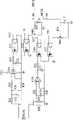
图3本实用新型无损伤快速均衡充电器电路原理图;Fig. 3 schematic diagram of the circuit of the non-damaging fast equalization charger of the utility model;
图4本实用新型无损伤快速均衡充电器集成有反极放电电路的二次斩波电路原理图;Fig. 4 The principle diagram of the secondary chopper circuit integrated with the reverse polarity discharge circuit of the utility model non-damage fast equalization charger;
图5本实用新型无损伤快速均衡充电器蓄电池动态参数采样电路原理图;Fig. 5 is the principle diagram of the dynamic parameter sampling circuit of the storage battery of the non-damage fast equalization charger of the utility model;
图6本实用新型无损伤快速均衡充电器的控制策略示意图。Fig. 6 is a schematic diagram of the control strategy of the non-damaging fast equalization charger of the utility model.
图1-6是本实用新型的最佳实施例。图3中:J1市电接口,U1保护电路模块,U2、U3滤波整流模块,U4功率因数校正模块,U5半桥电路驱动模块,U6、U7、U8蓄电池参数动态采样模块,U9、U10、U11集成有反极放电电路的二次斩波电路模块,U12,U15,U16,U17,U19,U20,U21隔离器件;U13功率开关管驱动芯片;U14可控电子负载;U18运算放大器;K1、K2、K3、K4、K5、K6可控开关模块,VCC辅助电源,MCU1-13微处理单元引脚与模块控制端接口,BAT1、BATN单个电池,BATK若干电池(>=1),R1-34电阻,WR1-2电位器,Q1、Q2,Q5,Q6,Q7驱动功率管,Q3,Q4,Q8,Q9三极管,C1-C15电容,D1、D2,D5-8,D10,D11齐纳二极管,D3、D4,D9,D12-16肖特基二极管,EC1-7电解电容,L1共模滤波电感,L2-4稳压续流电感,T1半桥变压器。Fig. 1-6 is the preferred embodiment of the present utility model. In Figure 3: J1 mains interface, U1 protection circuit module, U2, U3 filter rectification module, U4 power factor correction module, U5 half-bridge circuit driver module, U6, U7, U8 battery parameter dynamic sampling module, U9, U10, U11 Secondary chopper circuit module integrated with reverse pole discharge circuit, U12, U15, U16, U17, U19, U20, U21 isolation devices; U13 power switch tube drive chip; U14 controllable electronic load; U18 operational amplifier; K1, K2 , K3, K4, K5, K6 controllable switch modules, VCC auxiliary power supply, MCU1-13 micro-processing unit pins and module control terminal interface, BAT1, BATN single battery, BATK several batteries (>=1), R1-34 resistor , WR1-2 potentiometer, Q1, Q2, Q5, Q6, Q7 drive power tube, Q3, Q4, Q8, Q9 transistor, C1-C15 capacitor, D1, D2, D5-8, D10, D11 zener diode, D3 , D4, D9, D12-16 Schottky diodes, EC1-7 electrolytic capacitors, L1 common-mode filter inductors, L2-4 regulator freewheeling inductors, T1 half-bridge transformers.
具体实施方式Detailed ways
下面结合图1-6对本实用新型的无损伤快速均衡充电器作进一步详细说明:Below in conjunction with Figure 1-6, the damage-free fast equalization charger of the present invention will be further described in detail:
如图1所示为本实用新型无损伤快速均衡充电器内部结构框图,包括市电接口,保护电路,滤波电路,整流电路,功率因数校正电路,智能半桥斩波电路,滤波稳压稳流电路,充电接口,反极放电电路,蓄电池参数动态采样电路和微处理单元;其中,市电接口与保护电路相连,保护电路与滤波电路相连,滤波电路与整流电路相连,整流电路与功率因数校正电路相连,功率因数校正电路与智能半桥斩波电路相连,智能半桥斩波电路与滤波稳压稳流电路和微处理单元相连,滤波稳压稳流电路与充电接口相连,充电接口与蓄电池参数动态采样电路和反极放电电路相连,蓄电池参数动态采样电路与微处理单元相连,微处理单元与反极放电电路相连。其中,智能半桥电路包括一路一次斩波模块,多路二次斩波模块;蓄电池参数动态采样电路由多路蓄电池参数动态采样模块组成;反极放电电路由多路反极放电电路模块组成,并集成于多路二次斩波模块和一次斩波模块中。As shown in Figure 1, it is a block diagram of the internal structure of the non-damaging fast equalization charger of the present invention, including a mains interface, a protection circuit, a filter circuit, a rectifier circuit, a power factor correction circuit, an intelligent half-bridge chopper circuit, and a filter to stabilize voltage and stabilize current. circuit, charging interface, reverse pole discharge circuit, battery parameter dynamic sampling circuit and micro-processing unit; among them, the mains interface is connected with the protection circuit, the protection circuit is connected with the filter circuit, the filter circuit is connected with the rectification circuit, and the rectification circuit is connected with the power factor correction The circuit is connected, the power factor correction circuit is connected with the intelligent half-bridge chopper circuit, the intelligent half-bridge chopper circuit is connected with the filtering voltage stabilizing and current stabilizing circuit and the micro processing unit, the filtering stabilizing voltage stabilizing circuit is connected with the charging interface, and the charging interface is connected with the battery The parameter dynamic sampling circuit is connected with the reverse pole discharge circuit, the accumulator parameter dynamic sampling circuit is connected with the micro processing unit, and the micro processing unit is connected with the reverse pole discharge circuit. Among them, the intelligent half-bridge circuit includes one primary chopping module and multiple secondary chopping modules; the battery parameter dynamic sampling circuit is composed of multiple battery parameter dynamic sampling modules; the reverse pole discharge circuit is composed of multiple reverse pole discharge circuit modules, And integrated in the multi-channel secondary chopping module and the primary chopping module.
如图2所示为本实用新型无损伤快速均衡充电器内部智能半桥斩波电路结构框图,包括一个一次斩波电路,多路二次斩波电路,一个一次斩波电路控制开关K,多路二次斩波电路控制开关J,开关L,电容C1,Cn等。其中微处理单元根据蓄电池参数动态采样信息,控制开关K,开关J和开关L以决定是否进行隔离充电,多路二次斩波模块电路之间都接有格直电容C1和Cn,保证隔离充电的安全进行。As shown in Figure 2, it is a block diagram of the structure of the intelligent half-bridge chopper circuit inside the non-damaging fast equalization charger of the present invention, including a primary chopper circuit, multiple secondary chopper circuits, a primary chopper circuit control switch K, and multiple The secondary chopper circuit of the road controls switch J, switch L, capacitor C1, Cn and so on. Among them, the micro-processing unit dynamically samples information according to the battery parameters, controls the switch K, switch J and switch L to determine whether to carry out isolated charging, and the multi-channel secondary chopper module circuits are connected with grid capacitors C1 and Cn to ensure isolated charging safe conduct.
如图3所示为本实用新型无损伤快速均衡充电器电路原理图,市电经市电接口J1接入,通过保护电路模块U1进行过流检测,若出现过流现象,则切断市电;否则经共轭滤波电感L1进入滤波整流模块U2、U3,整流输出后进入功率因数校正模块U4,功率因数校正完毕进入智能半桥斩波模块;As shown in Figure 3, it is the schematic diagram of the non-damaging fast equalizing charger circuit of the present invention. The mains power is connected through the mains interface J1, and the overcurrent detection is performed through the protection circuit module U1. If an overcurrent phenomenon occurs, the mains power is cut off; Otherwise, it enters the filter and rectifier modules U2 and U3 through the conjugate filter inductor L1, and enters the power factor correction module U4 after the rectification output, and enters the intelligent half-bridge chopper module after the power factor correction is completed;
智能半桥斩波模块包括一个一次斩波模块,多路二次斩波模块U9、U10、U11,开关K1-K6,各路模块辅助电源均采用VCC,微处理单元MCU3输出信号控制开关K1,微处理单元MCU4输出信号控制开关K2,微处理单元MCU5输出信号控制开关K4,微处理单元MCU6输出信号控制开关K5,微处理单元MCU7输出信号控制开关K6,微处理单元MCU1输出信号控制开关K3,微处理单元MCU2输出信号控制反极放电电路模块U12;The intelligent half-bridge chopping module includes a primary chopping module, multi-channel secondary chopping modules U9, U10, U11, switches K1-K6, the auxiliary power supply of each module uses VCC, and the output signal of the micro-processing unit MCU3 controls the switch K1. Micro-processing unit MCU4 output signal control switch K2, micro-processing unit MCU5 output signal control switch K4, micro-processing unit MCU6 output signal control switch K5, micro-processing unit MCU7 output signal control switch K6, micro-processing unit MCU1 output signal control switch K3, The output signal of the micro-processing unit MCU2 controls the reverse pole discharge circuit module U12;
一次斩波模块和多路二次斩波模块均采用半桥式架构,以一次斩波模块中的半桥电路为例,包括半桥驱动电路模块U5,两个功率开关管Q1、Q2及其滤波吸收电路,一个半桥变压器和后级整流电路。电阻R5与二极管D3并联串接电容C1作为吸收电路并接在功率开关管Q1两端,电阻R6与二极管D4并联串接电容C2作为吸收电路并接在功率开关管Q2两端;功率开关管Q1和Q2的控制极和发射极之间分别串接电阻R3和电阻R4,半桥驱动模块U5分别串接电阻R1和电阻R2接入功率开关管Q1和功率开关管Q2的控制极进行驱动,功率开关管Q1和Q2的两端并接有齐纳二极管D1和D2;两个功率开关管Q1和Q2串接后并接于回路中;电解电容EC1和EC2分别并接电阻R7和R8,并以串接形式并于回路两端,半桥变压器T1初级的同名端通过电容C3接到电解电容EC1的负极端,另一侧接到功率开关管Q1的发射极;半桥变压器T1副边的同名端(非中间抽头)串接电阻R9和电容C4,电阻R9和电容C4两端并接齐纳二极管D5;另一侧(非中间抽头)串接电阻R10和电容C5,电阻R10和电容C5两端并接齐纳二极管D6,齐纳二极管D5和D6串接于回路正极端连接滤波稳压稳流电路,半桥变压器T1的中间抽头接电源地;多路二次斩波电路模块的构架与之相同,只不过各器件参数有变化。Both the primary chopping module and the multi-channel secondary chopping module adopt a half-bridge structure. Taking the half-bridge circuit in the primary chopping module as an example, it includes the half-bridge drive circuit module U5, two power switch tubes Q1, Q2 and their Filter absorption circuit, a half-bridge transformer and post-stage rectification circuit. Resistor R5 and diode D3 are connected in parallel with capacitor C1 as an absorbing circuit and connected to both ends of power switch tube Q1; resistor R6 and diode D4 are connected in parallel and connected in series with capacitor C2 as an absorbing circuit and connected to both ends of power switch tube Q2; power switch tube Q1 Resistor R3 and resistor R4 are respectively connected in series between the control electrode and the emitter electrode of Q2, and the half-bridge drive module U5 is respectively connected in series with resistor R1 and resistor R2 to connect to the control electrodes of power switch tube Q1 and power switch tube Q2 for driving. Both ends of the switching tubes Q1 and Q2 are connected in parallel with zener diodes D1 and D2; the two power switching tubes Q1 and Q2 are connected in series and connected in the loop; electrolytic capacitors EC1 and EC2 are connected in parallel with resistors R7 and R8 respectively, and connected in parallel with It is connected in series and at both ends of the circuit. The primary side of the half-bridge transformer T1 with the same name is connected to the negative terminal of the electrolytic capacitor EC1 through the capacitor C3, and the other side is connected to the emitter of the power switch tube Q1; the secondary side of the half-bridge transformer T1 has the same name. Resistor R9 and capacitor C4 are connected in series at one side (non-middle tap), and Zener diode D5 is connected in parallel at both ends of resistor R9 and capacitor C4; resistor R10 and capacitor C5 are connected in series at the other side (non-middle tap), resistor R10 and capacitor C5 are two Terminals are connected in parallel with Zener diode D6, Zener diodes D5 and D6 are connected in series to the positive end of the loop to connect to the filter voltage and current stabilization circuit, and the middle tap of the half-bridge transformer T1 is connected to the power ground; the structure of the multi-channel secondary chopper circuit module and The same, but the parameters of each device have changed.
滤波稳压稳流电路由电感L2,L3,电解电容EC3、EC4和齐纳二极管D7,D8组成;电感L2,L3串接于齐纳二极管D5和D6的输出侧,电感L2和L3的输出端与电源地之间并接电解电容EC3,EC4;齐纳二极管D7,D8并接后串接于电感L3的输出端。The filtering voltage stabilizing and current stabilizing circuit is composed of inductors L2, L3, electrolytic capacitors EC3, EC4 and Zener diodes D7, D8; inductors L2, L3 are connected in series to the output side of Zener diodes D5 and D6, and the output terminals of inductors L2 and L3 Electrolytic capacitors EC3 and EC4 are connected in parallel with the power ground; Zener diodes D7 and D8 are connected in parallel and then connected in series to the output end of the inductor L3.
滤波稳压稳流电路输出端分别接有可控开关K3-K6,可控开关K3的3脚接蓄电池充电接口的正极侧;另外还接反极放电模块U12的3脚;可控开关K4-K6的输出端1脚分别接二次斩波电路模块U9、U10、U11的2脚,二次斩波电路模块U9、U10、U11的1脚分别接单体蓄电池接口的正极侧,且可控开关K4-K6之间的接地端与1脚之间串有隔直电容C6,C7,蓄电池接口之间串接可控开关K1和K2;二次斩波电路模块U9、U10、U11中均集成有反极放电电路;另外,单体蓄电池接口的正极侧接入蓄电池参数动态采样模块。The output terminals of the filtering, voltage stabilizing and current stabilizing circuit are respectively connected with controllable switches K3-K6, and the 3 pins of the controllable switch K3 are connected to the positive side of the battery charging interface; in addition, the 3 pins of the reverse discharge module U12 are connected; the controllable switches K4-
蓄电池参数动态采样模块包括U6、U7、U8,其2脚均接入蓄电池接口正极侧。The battery parameter dynamic sampling module includes U6, U7, U8, and its 2 pins are all connected to the positive side of the battery interface.
微处理单元MCU通过其1-10各引脚,根据蓄电池参数动态采样模块U6、U7、U8的反馈信息,控制开关K1-K6的开关时机,已决定多路二次斩波模块U9、U10、U11的动作时机,以及它们内部集成的反极放电电路和一次斩波反极放电电路模块U12的动作时机。The micro-processing unit MCU controls the switching timing of the switches K1-K6 through its pins 1-10 according to the feedback information of the battery parameter dynamic sampling modules U6, U7, and U8, and has determined that the multi-channel secondary chopping modules U9, U10, The action timing of U11, and the action timing of their internal integrated anti-polarity discharge circuit and primary chopper anti-polarity discharge circuit module U12.
如图4所示为本实用新型无损伤快速均衡充电器集成有反极放电电路的二次斩波电路原理图;As shown in Figure 4, it is a schematic diagram of a secondary chopper circuit integrated with a reverse pole discharge circuit in the non-damaging fast equalization charger of the present invention;
其中任一路二次斩波电路包括电阻R11-R18、三极管Q3、Q4、Q8、Q9,功率开关管Q5、Q6,电容C8-C11、电解电容EC6、EC7,电感L4,肖特基二极管D9、D12、D13、D14,齐纳二极管D10、D11,功率开关管驱动芯片U13,光隔离器件U12、U15,微处理单元接口MCU11,MCU12和电源VCC;Any secondary chopper circuit includes resistors R11-R18, transistors Q3, Q4, Q8, Q9, power switch tubes Q5, Q6, capacitors C8-C11, electrolytic capacitors EC6, EC7, inductor L4, Schottky diodes D9, D12, D13, D14, zener diodes D10, D11, power switch tube driver chip U13, optical isolation devices U12, U15, micro-processing unit interface MCU11, MCU12 and power supply VCC;
反极放电电路包括电阻R19-R21,三极管Q10、Q11,功率开关管Q7,可控电子负载U14,电源VCC和微处理单元接口MCU13;The reverse pole discharge circuit includes resistors R19-R21, triodes Q10, Q11, power switch tube Q7, controllable electronic load U14, power supply VCC and micro-processing unit interface MCU13;
微处理单元MCU通过引脚11经由隔离器件U12接电阻R11到达信号地,产生的PWM方波,采用图腾柱式输出方式驱动功率开关管驱动芯片U13,图腾柱由三极管Q3、Q4组成,三极管Q3的集电极接VCC,同时与功率开关管驱动芯片U13的1脚相连;三极管Q3的发射极与三极管Q4的发射极相连,并接入功率开关管驱动芯片U13的2脚,三极管Q3和三极管Q4的基极相连,并经由电阻R12接电源地,三极管Q4的集电极接电源地,同时还接功率开关管驱动芯片U13的3脚,功率开关管驱动芯片U13的1脚和3脚之间并接电解电容EC6和电容C8,功率开关管驱动芯片U13的1脚和8脚之间接肖特基二极管D9,功率开关管驱动芯片U13的6脚和8脚接电容C9,功率开关管驱动芯片U13的7脚和6脚之间接有齐纳二极管D10、D11,功率开关管驱动芯片U13的6脚和电源地之间接有反向肖特基二极管D14,肖特基二极管D12、电容C10、电阻R13并联,肖特基二极管D12反向端接功率开关管驱动芯片U13的7脚,正向端接功率开关管Q5的门极,同时通过电阻R14接功率开关管驱动芯片U13的6脚;功率开关管Q5的一端接电源VCC,另一端经由滤波电感L4,肖特基二极管D13接蓄电池的正极侧,蓄电池的负极侧接有功率开关管Q6,蓄电池正极和负极之间并接电解电容EC7和电容C11,功率开关管Q6也采用图腾柱式输出驱动,图腾柱由三极管Q8和三极管Q9、电阻R16-R18以及电源VCC和隔离器件U15组成;微处理单元MCU的引脚12经由隔离器件U15通过电阻R15接信号地;蓄电池的正极和负极侧还串接有可控电子负载U14和功率开关管Q7,功率开关管Q7也采用图腾柱式输出驱动,图腾柱由三极管Q10、三极管Q11,电阻R20-22以及电源VCC和隔离器件U16组成;微处理单元MCU的引脚13经由隔离期间U16通过电阻R19接地。The micro-processing unit MCU reaches the signal ground through the pin 11 via the isolation device U12 connected to the resistor R11, and the generated PWM square wave uses the totem pole output mode to drive the power switch tube driver chip U13. The totem pole is composed of triodes Q3 and Q4, and the triode Q3 The collector is connected to VCC, and connected to
如图5所示为本实用新型无损伤快速均衡充电器蓄电池动态参数采样电路原理图;其中只给出了电流电压采样原理图,温度采样采用经典的温度采样电路,除采用耐腐的传感器外,采样电路并无差异,不再详述;蓄电池的正极侧接有电压采样电路,负极侧接有电流采样电路,两种采样电路均有隔离器件.As shown in Figure 5, it is the schematic diagram of the dynamic parameter sampling circuit of the storage battery of the non-damage fast equalization charger of the present invention; only the current and voltage sampling schematic diagram is given, and the temperature sampling adopts the classic temperature sampling circuit, except for the use of corrosion-resistant sensors. , there is no difference in the sampling circuit, and will not be described in detail; the positive side of the battery is connected to a voltage sampling circuit, and the negative side is connected to a current sampling circuit, and both sampling circuits have isolation devices.
电压采样电路包括电阻R28-R34、电容C14-C17、电位器WR1、运算放大器U18的5脚,6脚和7脚、光隔离器件U20、U21,电源VCC、+5V及微处理单元接口MCUk,电压采样电路分为两路一路串接电阻R23,电阻R25接入运算放电器U18的正反馈端,另一路串接电阻R26接运算放大器U18的负反馈端,运算放大器U18的正反馈端和负反馈端还并接有电阻R24,电容C12一端接地,另一端接电阻R23的输出端,运算放大器U18的电源接VCC,4脚接电源地,1脚串接电阻R27经由两路隔离器件U17和隔离器件U19接电源地,运算放大器U18的1脚和2脚之间还并接有电容C13,隔离器件U17的受激发端一侧接电源VCC,另一侧接运算放大器U18的2脚;隔离器件U19的受激发端一侧接电源+5V,另一侧通过串接电位器WR2接信号地,电位器WR2的中端接电阻R33,从电阻R33输出的电压信号与微处理单元的引脚8、9或10相连,而且在引脚与信号地之间并接电容C16。The voltage sampling circuit includes resistors R28-R34, capacitors C14-C17, potentiometer WR1,
电流采样电路包括电阻R28-R34,电容C14-C17,电位器WR1,运算放大器U18的5脚,6脚和7脚,光隔离器件U20,U21,电源VCC,+5V及微处理单元接口MCUk,电流采样电路分为两路,一路串接电阻R31,接入运算放电器U18的正反馈端,另一路经由并联的两个功率电阻R28和R29串接电阻R30接运算放大器U18的负反馈端,电容C14一端接地,另一端接蓄电池负极侧,运算放大器U18的7脚串接电阻R32经由两路隔离器件U20,U21接电源地,运算放大器U18的7脚和6脚之间还并接有电容C15,隔离器件U20的受激发端一侧接电源VCC,另一侧接运算放大器的6脚;隔离器件U21的受激发端一侧接电源+5V,另一侧通过串接电位器WR1接信号地,电位器WR1的中端接电阻R34,从电阻R34输出的电压信号与微处理单元的引脚8、9或10相连,而且与引脚与信号地之间并接电容C17。The current sampling circuit includes resistors R28-R34, capacitors C14-C17, potentiometer WR1, pins 5, 6 and 7 of the operational amplifier U18, optical isolation devices U20, U21, power supply VCC, +5V and micro-processing unit interface MCUk, The current sampling circuit is divided into two circuits, one of which is connected in series with resistor R31 and connected to the positive feedback terminal of operational discharger U18, and the other is connected to the negative feedback terminal of operational amplifier U18 via two power resistors R28 and R29 in parallel connected in series with resistor R30. One end of the capacitor C14 is grounded, and the other end is connected to the negative side of the battery. The 7-pin of the operational amplifier U18 is connected in series with the resistor R32 via two isolation devices U20, U21 is connected to the power ground, and a capacitor is connected in parallel between the 7-pin and 6-pin of the operational amplifier U18 C15, one side of the excited end of the isolation device U20 is connected to the power supply VCC, and the other side is connected to the 6 pin of the operational amplifier; one side of the excited end of the isolation device U21 is connected to the power supply +5V, and the other side is connected to the signal through the serial potentiometer WR1 Ground, the potentiometer WR1 is connected to the resistor R34, the voltage signal output from the resistor R34 is connected to the pin 8, 9 or 10 of the micro-processing unit, and the capacitor C17 is connected in parallel between the pin and the signal ground.
如图6所示为本实用新型无损伤快速均衡充电器控制策略流程图,具体控制策略是:开始上电进行系统初始化,软件初始化,硬件初始化,过流检查等操作,若出现系统异常或是过流警告则切断市电,否则微处理单元发出控制信号启动蓄电池参数动态采集电路,获取蓄电池初始状态参数,微处理单元根据采样值判断是否进行蓄电池预充电,若需要预充电,则先进入预充电状态,否则微处理单元根据采样值计算出的蓄电池最大初始充电可接受电流开始大电流快速充电;快速充电过程中,微处理单元随时根据采样值计算并判定各单体蓄电池参数是否超出预设一致性要求上限,若是则启动多路二次斩波电路开关,进行隔离充电,否则,继续整体充电过程;隔离充电过程中,微处理单元随时监测蓄电池参数动态采样值,若各单体蓄电池参数动态采样值满足停充要求则停止充电过程,否则,继续隔离充电过程。As shown in Figure 6, the flow chart of the control strategy of the non-damage fast equalization charger of the present invention is shown. The specific control strategy is: start power-on for system initialization, software initialization, hardware initialization, over-current inspection and other operations. If there is a system abnormality or If there is an over-current warning, the mains power will be cut off, otherwise the micro-processing unit will send a control signal to start the dynamic acquisition circuit of battery parameters to obtain the initial state parameters of the battery. Otherwise, the micro-processing unit calculates the battery’s maximum initial charge acceptable current based on the sampling value and starts high-current fast charging; during the fast charging process, the micro-processing unit calculates and judges whether the parameters of each single battery exceed the preset value at any time according to the sampling value Consistency requires the upper limit, if so, start the multi-channel secondary chopper circuit switch to carry out isolated charging, otherwise, continue the overall charging process; during the isolated charging process, the micro-processing unit monitors the dynamic sampling value of the battery parameters at any time, if the parameters of each single battery If the dynamic sampling value meets the charging stop requirement, the charging process will be stopped; otherwise, the isolated charging process will continue.
控制策略一些细节的描述:蓄电池进行大电流快速充电和隔离充电时,蓄电池各项参数,如端电压,温升变化率等都需要满足一定的上限阈值才能达到无损伤充电,一般端电压的上限为析气率为0.05%的蓄电池开路电压,温升变化率的上限为不超过1-6个温升变化单位;大电流快速充电和隔离充电过程中,微处理单元根据实验获得的经验值进行正负脉冲充电,一是解决充电过程中迅速上升的极化问题;二是维持蓄电池允许初始最大可充电电流值,加快充电过程。The description of some details of the control strategy: When the battery is charged with high current fast charging and isolated charging, various parameters of the battery, such as terminal voltage, temperature rise change rate, etc., need to meet a certain upper limit threshold to achieve non-damage charging. Generally, the upper limit of the terminal voltage The open-circuit voltage of the battery with a gassing rate of 0.05%, the upper limit of the temperature rise change rate is no more than 1-6 temperature rise change units; in the process of high-current fast charging and isolated charging, the micro-processing unit performs the test according to the empirical value obtained from the experiment. Positive and negative pulse charging, one is to solve the polarization problem that rises rapidly during the charging process; the other is to maintain the initial maximum chargeable current value of the battery and speed up the charging process.
以上所述,仅是本实用新型的较佳实施例而已,并非是对本实用新型作其它形式的限制,任何熟悉本专业的技术人员可能利用上述揭示的技术内容加以变更或改型为等同变化的等效实施例。但是凡是未脱离本实用新型技术方案内容,依据本实用新型的技术实质对以上实施例所作的任何简单修改、等同变化与改型,仍属于本实用新型技术方案的保护范围。The above is only a preferred embodiment of the utility model, and is not intended to limit the utility model in other forms. Any skilled person who is familiar with this profession may use the technical content disclosed above to change or remodel it into an equivalent change. Equivalent embodiment. However, any simple modifications, equivalent changes and modifications made to the above embodiments according to the technical essence of the present utility model without departing from the content of the technical solution of the utility model still belong to the protection scope of the technical solution of the utility model.
Claims (4)
Translated fromChinesePriority Applications (1)
| Application Number | Priority Date | Filing Date | Title |
|---|---|---|---|
| CN2010202384643UCN201742140U (en) | 2010-06-28 | 2010-06-28 | Harmless quick balanced charger for storage batteries |
Applications Claiming Priority (1)
| Application Number | Priority Date | Filing Date | Title |
|---|---|---|---|
| CN2010202384643UCN201742140U (en) | 2010-06-28 | 2010-06-28 | Harmless quick balanced charger for storage batteries |
Publications (1)
| Publication Number | Publication Date |
|---|---|
| CN201742140Utrue CN201742140U (en) | 2011-02-09 |
Family
ID=43557418
Family Applications (1)
| Application Number | Title | Priority Date | Filing Date |
|---|---|---|---|
| CN2010202384643UExpired - Fee RelatedCN201742140U (en) | 2010-06-28 | 2010-06-28 | Harmless quick balanced charger for storage batteries |
Country Status (1)
| Country | Link |
|---|---|
| CN (1) | CN201742140U (en) |
Cited By (4)
| Publication number | Priority date | Publication date | Assignee | Title |
|---|---|---|---|---|
| CN101872990A (en)* | 2010-06-28 | 2010-10-27 | 山东申普汽车控制技术有限公司 | Storage battery non-damage rapid balanced charger and control strategy thereof |
| CN102842945A (en)* | 2011-06-22 | 2012-12-26 | 河南泰兰特电子科技有限公司 | Intelligent charger for storage battery |
| CN103364737A (en)* | 2012-03-26 | 2013-10-23 | 鸿富锦精密工业(深圳)有限公司 | Power capacitive-load testing device |
| CN120056802A (en)* | 2025-03-28 | 2025-05-30 | 广东省科学院电子电器研究所 | Balanced management system for monitoring state of power battery |
- 2010
- 2010-06-28CNCN2010202384643Upatent/CN201742140U/ennot_activeExpired - Fee Related
Cited By (5)
| Publication number | Priority date | Publication date | Assignee | Title |
|---|---|---|---|---|
| CN101872990A (en)* | 2010-06-28 | 2010-10-27 | 山东申普汽车控制技术有限公司 | Storage battery non-damage rapid balanced charger and control strategy thereof |
| CN101872990B (en)* | 2010-06-28 | 2013-07-17 | 山东申普交通科技有限公司 | Control strategy of storage battery non-damage rapid balanced charger |
| CN102842945A (en)* | 2011-06-22 | 2012-12-26 | 河南泰兰特电子科技有限公司 | Intelligent charger for storage battery |
| CN103364737A (en)* | 2012-03-26 | 2013-10-23 | 鸿富锦精密工业(深圳)有限公司 | Power capacitive-load testing device |
| CN120056802A (en)* | 2025-03-28 | 2025-05-30 | 广东省科学院电子电器研究所 | Balanced management system for monitoring state of power battery |
Similar Documents
| Publication | Publication Date | Title |
|---|---|---|
| CN101872990B (en) | Control strategy of storage battery non-damage rapid balanced charger | |
| CN201742140U (en) | Harmless quick balanced charger for storage batteries | |
| CN203243061U (en) | MPPT solar controller | |
| CN204407987U (en) | A kind of reparation formula pulse charger | |
| CN206517086U (en) | A kind of self-adaption constant power charger | |
| CN2427918Y (en) | Novel, quick action and pulsation charging device | |
| CN211765363U (en) | Vehicle-mounted intelligent power management system based on CAN bus | |
| CN201570884U (en) | Pulse charger | |
| CN204167905U (en) | A kind of emergency power supply against short-circuit protection system | |
| CN203984073U (en) | The battery system of separate redundancy each other | |
| CN204103591U (en) | A kind of ambulance-mounted supply unit | |
| CN103956531B (en) | Super-high current peak pulse charging control method for lead-acid batteries | |
| CN203278303U (en) | Lithium iron phosphate emergency power supply with short-circuit protection function | |
| CN202888916U (en) | Multifunctional charging device capable of automatically identifying voltage | |
| CN202712938U (en) | A high-frequency chopper boost charging circuit | |
| CN205178601U (en) | Storage battery charging power | |
| CN204349564U (en) | Solar recharging all-in-one | |
| CN204119017U (en) | A kind of soft start protective circuit for charging device | |
| CN207251496U (en) | A kind of H bridges chopper circuit | |
| CN107968473A (en) | A kind of intelligent electric automobile discharge and recharge stake | |
| CN203871911U (en) | Storage battery charger | |
| CN203026966U (en) | Bidirectional lossless equalization circuit based on forward DC/DC converter | |
| CN203554037U (en) | Electric bicycle wireless pulse charging system | |
| CN102593911B (en) | Photovoltaic charging circuit having synchronized reverse isolation function | |
| CN202949267U (en) | Intelligent fast and slow charger |
Legal Events
| Date | Code | Title | Description |
|---|---|---|---|
| C14 | Grant of patent or utility model | ||
| GR01 | Patent grant | ||
| C56 | Change in the name or address of the patentee | Owner name:SHANDONG SHENPU COMMUNICATION TECHNOLOGY CO., LTD. Free format text:FORMER NAME: SHANDONG SHENPU AUTOMOTIVE CONTROL TECHNOLOGY CO., LTD. | |
| CP03 | Change of name, title or address | Address after:255086 room 521, building E, hi tech Pioneer Park, Zibo hi tech Industrial Development Zone, Zibo, Shandong Patentee after:Shandong Shenpu Traffic Technology Co., Ltd. Address before:255086 room 521, building E, hi tech Pioneer Park, hi tech Industrial Development Zone, Shandong, Zibo Patentee before:Shandong Shenpu Automotive Control Technology Co., Ltd. | |
| CF01 | Termination of patent right due to non-payment of annual fee | Granted publication date:20110209 Termination date:20160628 | |
| CF01 | Termination of patent right due to non-payment of annual fee |