CN201681935U - Non-paddle multiturn pin static release ring passive device packaging structure - Google Patents
Non-paddle multiturn pin static release ring passive device packaging structureDownload PDFInfo
- Publication number
- CN201681935U CN201681935UCN2010201826073UCN201020182607UCN201681935UCN 201681935 UCN201681935 UCN 201681935UCN 2010201826073 UCN2010201826073 UCN 2010201826073UCN 201020182607 UCN201020182607 UCN 201020182607UCN 201681935 UCN201681935 UCN 201681935U
- Authority
- CN
- China
- Prior art keywords
- pin
- release ring
- static release
- chip
- passive device
- Prior art date
- Legal status (The legal status is an assumption and is not a legal conclusion. Google has not performed a legal analysis and makes no representation as to the accuracy of the status listed.)
- Expired - Lifetime
Links
- 230000003068static effectEffects0.000titleclaimsabstractdescription25
- 238000004806packaging method and processMethods0.000titleabstractdescription12
- 239000002184metalSubstances0.000claimsabstractdescription52
- 229910052751metalInorganic materials0.000claimsabstractdescription52
- 239000000945fillerSubstances0.000claimsdescription14
- 239000000463materialSubstances0.000claimsdescription9
- 239000005022packaging materialSubstances0.000claimsdescription6
- 230000002093peripheral effectEffects0.000claims1
- 238000000465mouldingMethods0.000abstractdescription18
- 150000001875compoundsChemical class0.000abstractdescription17
- 239000000126substanceSubstances0.000abstractdescription4
- 239000002699waste materialSubstances0.000abstractdescription3
- OKTJSMMVPCPJKN-UHFFFAOYSA-NCarbonChemical compound[C]OKTJSMMVPCPJKN-UHFFFAOYSA-N0.000abstract1
- 229910052799carbonInorganic materials0.000abstract1
- 239000002313adhesive filmSubstances0.000description13
- 238000000034methodMethods0.000description12
- 239000000758substrateSubstances0.000description8
- 238000012858packaging processMethods0.000description7
- 238000010586diagramMethods0.000description6
- 238000005516engineering processMethods0.000description5
- 239000000853adhesiveSubstances0.000description4
- 230000001070adhesive effectEffects0.000description4
- 238000005530etchingMethods0.000description4
- 230000003071parasitic effectEffects0.000description4
- 238000003486chemical etchingMethods0.000description3
- 229940126214compound 3Drugs0.000description3
- 238000009713electroplatingMethods0.000description3
- 238000007789sealingMethods0.000description3
- 238000004364calculation methodMethods0.000description2
- 230000005496eutecticsEffects0.000description2
- PCHJSUWPFVWCPO-UHFFFAOYSA-NgoldChemical compound[Au]PCHJSUWPFVWCPO-UHFFFAOYSA-N0.000description2
- 238000004519manufacturing processMethods0.000description2
- 239000011347resinSubstances0.000description2
- 229920005989resinPolymers0.000description2
- 239000000565sealantSubstances0.000description2
- 229910000679solderInorganic materials0.000description2
- 238000003860storageMethods0.000description2
- 206010034701Peroneal nerve palsyDiseases0.000description1
- 230000009286beneficial effectEffects0.000description1
- 239000008393encapsulating agentSubstances0.000description1
- 230000007613environmental effectEffects0.000description1
- 239000010931goldSubstances0.000description1
- 229910052737goldInorganic materials0.000description1
- 230000035515penetrationEffects0.000description1
- 239000004065semiconductorSubstances0.000description1
- 238000004904shorteningMethods0.000description1
- 239000007779soft materialSubstances0.000description1
- 238000005476solderingMethods0.000description1
- 238000003466weldingMethods0.000description1
Images


Classifications
- H—ELECTRICITY
- H01—ELECTRIC ELEMENTS
- H01L—SEMICONDUCTOR DEVICES NOT COVERED BY CLASS H10
- H01L24/00—Arrangements for connecting or disconnecting semiconductor or solid-state bodies; Methods or apparatus related thereto
- H01L24/93—Batch processes
- H01L24/95—Batch processes at chip-level, i.e. with connecting carried out on a plurality of singulated devices, i.e. on diced chips
- H01L24/97—Batch processes at chip-level, i.e. with connecting carried out on a plurality of singulated devices, i.e. on diced chips the devices being connected to a common substrate, e.g. interposer, said common substrate being separable into individual assemblies after connecting
- H—ELECTRICITY
- H01—ELECTRIC ELEMENTS
- H01L—SEMICONDUCTOR DEVICES NOT COVERED BY CLASS H10
- H01L2224/00—Indexing scheme for arrangements for connecting or disconnecting semiconductor or solid-state bodies and methods related thereto as covered by H01L24/00
- H01L2224/01—Means for bonding being attached to, or being formed on, the surface to be connected, e.g. chip-to-package, die-attach, "first-level" interconnects; Manufacturing methods related thereto
- H01L2224/26—Layer connectors, e.g. plate connectors, solder or adhesive layers; Manufacturing methods related thereto
- H01L2224/31—Structure, shape, material or disposition of the layer connectors after the connecting process
- H01L2224/32—Structure, shape, material or disposition of the layer connectors after the connecting process of an individual layer connector
- H01L2224/321—Disposition
- H01L2224/32151—Disposition the layer connector connecting between a semiconductor or solid-state body and an item not being a semiconductor or solid-state body, e.g. chip-to-substrate, chip-to-passive
- H01L2224/32221—Disposition the layer connector connecting between a semiconductor or solid-state body and an item not being a semiconductor or solid-state body, e.g. chip-to-substrate, chip-to-passive the body and the item being stacked
- H01L2224/32245—Disposition the layer connector connecting between a semiconductor or solid-state body and an item not being a semiconductor or solid-state body, e.g. chip-to-substrate, chip-to-passive the body and the item being stacked the item being metallic
- H—ELECTRICITY
- H01—ELECTRIC ELEMENTS
- H01L—SEMICONDUCTOR DEVICES NOT COVERED BY CLASS H10
- H01L2224/00—Indexing scheme for arrangements for connecting or disconnecting semiconductor or solid-state bodies and methods related thereto as covered by H01L24/00
- H01L2224/01—Means for bonding being attached to, or being formed on, the surface to be connected, e.g. chip-to-package, die-attach, "first-level" interconnects; Manufacturing methods related thereto
- H01L2224/42—Wire connectors; Manufacturing methods related thereto
- H01L2224/47—Structure, shape, material or disposition of the wire connectors after the connecting process
- H01L2224/48—Structure, shape, material or disposition of the wire connectors after the connecting process of an individual wire connector
- H01L2224/481—Disposition
- H01L2224/48151—Connecting between a semiconductor or solid-state body and an item not being a semiconductor or solid-state body, e.g. chip-to-substrate, chip-to-passive
- H01L2224/48221—Connecting between a semiconductor or solid-state body and an item not being a semiconductor or solid-state body, e.g. chip-to-substrate, chip-to-passive the body and the item being stacked
- H01L2224/48245—Connecting between a semiconductor or solid-state body and an item not being a semiconductor or solid-state body, e.g. chip-to-substrate, chip-to-passive the body and the item being stacked the item being metallic
- H01L2224/48247—Connecting between a semiconductor or solid-state body and an item not being a semiconductor or solid-state body, e.g. chip-to-substrate, chip-to-passive the body and the item being stacked the item being metallic connecting the wire to a bond pad of the item
- H—ELECTRICITY
- H01—ELECTRIC ELEMENTS
- H01L—SEMICONDUCTOR DEVICES NOT COVERED BY CLASS H10
- H01L2224/00—Indexing scheme for arrangements for connecting or disconnecting semiconductor or solid-state bodies and methods related thereto as covered by H01L24/00
- H01L2224/73—Means for bonding being of different types provided for in two or more of groups H01L2224/10, H01L2224/18, H01L2224/26, H01L2224/34, H01L2224/42, H01L2224/50, H01L2224/63, H01L2224/71
- H01L2224/732—Location after the connecting process
- H01L2224/73251—Location after the connecting process on different surfaces
- H01L2224/73265—Layer and wire connectors
- H—ELECTRICITY
- H01—ELECTRIC ELEMENTS
- H01L—SEMICONDUCTOR DEVICES NOT COVERED BY CLASS H10
- H01L2224/00—Indexing scheme for arrangements for connecting or disconnecting semiconductor or solid-state bodies and methods related thereto as covered by H01L24/00
- H01L2224/93—Batch processes
- H01L2224/95—Batch processes at chip-level, i.e. with connecting carried out on a plurality of singulated devices, i.e. on diced chips
- H01L2224/97—Batch processes at chip-level, i.e. with connecting carried out on a plurality of singulated devices, i.e. on diced chips the devices being connected to a common substrate, e.g. interposer, said common substrate being separable into individual assemblies after connecting
- H—ELECTRICITY
- H01—ELECTRIC ELEMENTS
- H01L—SEMICONDUCTOR DEVICES NOT COVERED BY CLASS H10
- H01L24/00—Arrangements for connecting or disconnecting semiconductor or solid-state bodies; Methods or apparatus related thereto
- H01L24/73—Means for bonding being of different types provided for in two or more of groups H01L24/10, H01L24/18, H01L24/26, H01L24/34, H01L24/42, H01L24/50, H01L24/63, H01L24/71
- H—ELECTRICITY
- H01—ELECTRIC ELEMENTS
- H01L—SEMICONDUCTOR DEVICES NOT COVERED BY CLASS H10
- H01L2924/00—Indexing scheme for arrangements or methods for connecting or disconnecting semiconductor or solid-state bodies as covered by H01L24/00
- H01L2924/013—Alloys
- H01L2924/0132—Binary Alloys
- H01L2924/01322—Eutectic Alloys, i.e. obtained by a liquid transforming into two solid phases
- H—ELECTRICITY
- H01—ELECTRIC ELEMENTS
- H01L—SEMICONDUCTOR DEVICES NOT COVERED BY CLASS H10
- H01L2924/00—Indexing scheme for arrangements or methods for connecting or disconnecting semiconductor or solid-state bodies as covered by H01L24/00
- H01L2924/15—Details of package parts other than the semiconductor or other solid state devices to be connected
- H01L2924/181—Encapsulation
- H—ELECTRICITY
- H01—ELECTRIC ELEMENTS
- H01L—SEMICONDUCTOR DEVICES NOT COVERED BY CLASS H10
- H01L2924/00—Indexing scheme for arrangements or methods for connecting or disconnecting semiconductor or solid-state bodies as covered by H01L24/00
- H01L2924/19—Details of hybrid assemblies other than the semiconductor or other solid state devices to be connected
- H01L2924/191—Disposition
- H01L2924/19101—Disposition of discrete passive components
- H01L2924/19105—Disposition of discrete passive components in a side-by-side arrangement on a common die mounting substrate
Landscapes
- Engineering & Computer Science (AREA)
- Computer Hardware Design (AREA)
- Microelectronics & Electronic Packaging (AREA)
- Power Engineering (AREA)
- Packaging Frangible Articles (AREA)
Abstract
Description
Translated fromChinese(一)技术领域(1) Technical field
本实用新型涉及一种封装结构。属于半导体封装技术领域。The utility model relates to a packaging structure. It belongs to the technical field of semiconductor packaging.
(二)背景技术(2) Background technology
传统的封装结构主要有二种:There are two main types of traditional packaging structures:
第一种:The first:
采用金属基板的正面进行化学蚀刻及表面电镀层后,在金属基板的背面贴上一层耐高温的胶膜形成可以进行封装过程的引线框载体(如图3所示)。After chemical etching and surface electroplating are performed on the front of the metal substrate, a layer of high-temperature-resistant adhesive film is pasted on the back of the metal substrate to form a lead frame carrier that can be packaged (as shown in Figure 3).
第二种:The second type:
采用金属基板的正面进行化学蚀刻及表面电镀层后,即完成引线框的制作(如图4所示)。而引线框的背面则在封装过程中再进行背面蚀刻。After chemical etching and surface electroplating are carried out on the front side of the metal substrate, the production of the lead frame is completed (as shown in FIG. 4 ). The backside of the lead frame is then etched during the packaging process.
而上述的二种引线框在封装过程中存在了以下的不足点:However, the above two lead frames have the following disadvantages in the packaging process:
第一种:The first:
1)此种引线框架因背面必须要贴上一层昂贵可抗高温的胶膜。所以直接增加了高昂的成本。1) This kind of lead frame must be pasted with a layer of expensive and high temperature resistant adhesive film on the back. So directly increased the high cost.
2)也因为此种引线框架的背面必须要贴上一层可抗高温的胶膜,所以在封装过程中的装片工艺只能使用导电或是不导电的树脂工艺,而完全 不能采用共晶工艺以及软焊料的工艺进行装片,所以可选择的产品种类就有较大的局限性。2) Also because the back of this kind of lead frame must be pasted with a layer of adhesive film that can resist high temperature, so the chip loading process in the packaging process can only use conductive or non-conductive resin technology, and eutectic cannot be used at all. Process and soft solder process for mounting chips, so the types of products that can be selected are relatively limited.
3)又因为此种引线框架的背面必须要贴上一层可抗高温的胶膜,而在封装过程中的球焊键合工艺中,因为此可抗高温的胶膜是软性材质,所以造成了球焊键合参数的不稳定,严重的影响了球焊的质量与产品可靠度的稳定性。3) Because the back of this kind of lead frame must be pasted with a layer of high temperature resistant adhesive film, and in the ball soldering bonding process in the packaging process, because the high temperature resistant adhesive film is a soft material, so The instability of the ball bonding parameters is caused, which seriously affects the quality of the ball bonding and the stability of product reliability.
4)再因为此种引线框架的背面必须要贴上一层可抗高温的胶膜,而在封装过程中的塑封工艺过程,因为塑封的高压关系很容易造成引线框架与胶膜之间渗入塑封料,而将原本应属金属脚是导电的型态因为渗入了塑封料反而变成了绝缘脚(如图5所示)。4) Because the back of this kind of lead frame must be affixed with a layer of high-temperature-resistant adhesive film, and in the plastic sealing process during the packaging process, because of the high pressure of the plastic seal, it is easy to cause penetration between the lead frame and the adhesive film. material, and the originally metal pins are conductive because they are infiltrated with the molding compound but become insulating pins (as shown in Figure 5).
第二种:The second type:
此种引线框架结构在金属基板正面进行了半蚀刻工艺,虽然可以解决第一种引线框架的问题,但是因为只在金属基板正面进行了半蚀刻工作,而在塑封过程中塑封料只有包覆住半只脚的高度,所以塑封体与金属脚的束缚能力就变小了,如果塑封体贴片到PCB板上不是很好时,再进行返工重贴,就容易产生掉脚的问题(如图6所示)。This kind of lead frame structure has been half-etched on the front of the metal substrate. Although it can solve the problem of the first type of lead frame, because only half-etching is performed on the front of the metal substrate, the plastic encapsulant can only cover the front of the metal substrate. The height of half a foot, so the binding ability between the plastic package and the metal foot becomes smaller. If the plastic package is not attached to the PCB board well, it is easy to cause the problem of foot drop (as shown in the figure) 6).
尤其塑封料的种类是采用有填料时候,因为材料在生产过程的环境与后续表面贴装的应力变化关系,会造成金属与塑封料产生垂直型的裂缝,其特性是填料比例越高则越硬越脆越容易产生裂缝。Especially when the type of molding compound is filled, because the relationship between the environment of the material in the production process and the stress change of the subsequent surface mount will cause vertical cracks between the metal and the molding compound, the characteristic is that the higher the filler ratio, the harder it is The more brittle the easier it is to crack.
另外,由于芯片与引脚之间的距离较远,如图7~8所示,金属线的长度较长,金属线成本较高(尤其是昂贵的纯金质的金属线);同样由于金属 线的长度较长,使得芯片的信号输出速度较慢(由其是存储类的产品以及需要大量数据的计算,更为突出);也同样由于金属线的长度较长,所以金属线所存在的寄生电阻/寄生电容与寄生电杆对信号的干扰也较高;再由于芯片与引脚之间的距离较远,使得封装的体积与面积较大,材料成本较高,废弃物较多。In addition, due to the long distance between the chip and the pins, as shown in Figures 7-8, the length of the metal wire is longer, and the cost of the metal wire is higher (especially the expensive pure gold metal wire); The length of the wire is longer, which makes the signal output speed of the chip slower (it is more prominent because it is a storage product and the calculation that requires a large amount of data); also because the length of the metal wire is longer, the existence of the metal wire The interference of parasitic resistance/capacitance and parasitic poles on the signal is also high; and because the distance between the chip and the pins is long, the volume and area of the package are large, the cost of materials is high, and there is more waste.
(三)发明内容(3) Contents of the invention
本实用新型的目的在于克服上述不足,提供一种降低封装成本、可选择的产品种类广、球焊的质量与产品可靠度的稳定性好、塑封体与金属脚的束缚能力大的无基岛多圈脚静电释放圈无源器件封装结构。The purpose of this utility model is to overcome the above disadvantages, to provide a baseless island with reduced packaging cost, wide range of optional products, good ball welding quality and product reliability stability, and large binding capacity between the plastic package and the metal feet. The packaging structure of the passive device of the multi-turn static discharge ring.
本实用新型的目的是这样实现的:一种无基岛多圈脚静电释放圈无源器件封装结构,包括静电释放圈、引脚、不导电粘结物质、芯片、金属线和有填料塑封料,在所述静电释放圈和引脚的正面设置有第一金属层,在所述静电释放圈和引脚的背面设置有第二金属层,所述引脚设置有多圈,所述引脚正面延伸到静电释放圈旁边,在所述引脚外围的区域、引脚与静电释放圈之间的区域、静电释放圈内外的区域以及引脚与引脚之间的区域嵌置有无填料的塑封料,所述无填料的塑封料将引脚下部外围、引脚下部与静电释放圈下部、所述引脚正面延伸部分的背面以及引脚下部与引脚下部连接成一体,且使所述静电释放圈和引脚背面尺寸小于静电释放圈和引脚正面尺寸,形成上大下小的静电释放圈和引脚结构,在所述静电释放圈内的无填料塑封料正面通过不导电粘结物质设置有芯片,芯片正面与引脚 正面第一金属层之间用金属线连接,在引脚与引脚之间或引脚与静电释放圈之间跨接有无源器件,在所述静电释放圈和引脚的上部以及芯片、金属线和无源器件外包封有填料塑封料。The purpose of the utility model is achieved in this way: a baseless island multi-circle foot electrostatic release ring passive device packaging structure, including electrostatic release rings, pins, non-conductive adhesive substances, chips, metal wires and plastic packaging materials with fillers , a first metal layer is provided on the front of the electrostatic release ring and the pins, a second metal layer is provided on the back of the electrostatic discharge ring and the pins, the pins are provided with multiple turns, and the pins The front side extends next to the ESD ring, and the area around the pin, the area between the pin and the ESD ring, the area inside and outside the ESD ring, and the area between the pins are embedded with filler-free Molding compound, the filler-free molding compound connects the periphery of the lower part of the pin, the lower part of the pin and the lower part of the electrostatic discharge ring, the back of the front extension part of the pin, and the lower part of the pin and the lower part of the pin, and makes the The size of the electrostatic discharge ring and the back of the pin is smaller than the size of the electrostatic release ring and the front of the pin, forming a structure of the electrostatic discharge ring and the pin with a large top and a small bottom. The substance is provided with a chip, the front of the chip is connected with the first metal layer on the front of the pin with a metal wire, and a passive device is connected between the pin and the pin or between the pin and the electrostatic discharge ring, and the electrostatic discharge The upper parts of the rings and pins, as well as the chips, metal wires and passive components are encapsulated with filler molding compound.
本实用新型的有益效果是:The beneficial effects of the utility model are:
1)此种引线框的背面不须要贴上一层昂贵可抗高温的胶膜。所以直接降低了高昂的成本。1) The back of the lead frame does not need to be pasted with a layer of expensive and high temperature resistant adhesive film. Therefore, the high cost is directly reduced.
2)也因为此种引线框架的背面不须要贴上一层可抗高温的胶膜,所以在封装过程中的装片工艺除了能使用导电或是不导电的树脂工艺外,还能采用共晶工艺以及软焊料的工艺进行装片,所以可选择的产品种类就广。2) Also because the back of the lead frame does not need to be affixed with a layer of high-temperature-resistant adhesive film, the chip loading process in the packaging process can not only use conductive or non-conductive resin technology, but also eutectic Process and soft solder process for chip mounting, so a wide range of products can be selected.
3)又因为此种引线框架的背面不须要贴上一层可抗高温的胶膜,确保了球焊键合参数的稳定性,保证了球焊的质量与产品可靠度的稳定性。3) Because the back of the lead frame does not need to be pasted with a layer of high-temperature-resistant adhesive film, the stability of the bonding parameters of the ball bonding is ensured, and the quality of the ball bonding and the stability of the product reliability are guaranteed.
4)再因为此种引线框架不须要贴上一层可抗高温的胶膜,而在封装过程中的塑封工艺过程,完全不会造成引线框与胶膜之间渗入塑封料。4) Furthermore, because this kind of lead frame does not need to be pasted with a layer of high-temperature-resistant adhesive film, the plastic sealing process in the packaging process will not cause the plastic sealing compound to penetrate between the lead frame and the adhesive film at all.
5)由于在所述金属脚(引脚)与金属脚间的区域嵌置有无填料的软性填缝剂,该无填料的软性填缝剂与在塑封过程中的常规有填料塑封料一起包覆住整个金属脚的高度,所以塑封体与金属脚的束缚能力就变大了,不会再有产生掉脚的问题。5) Since there is no filler soft sealant embedded in the area between the metal feet (pins) and the metal feet, the filler-free soft sealant is different from the conventional filler molding compound in the molding process. Cover the entire height of the metal feet together, so the binding capacity between the plastic package and the metal feet becomes larger, and there will be no more problems of falling feet.
6)由于采用了正面与背面分开蚀刻作业的方法,所以在蚀刻作业中可形成背面静电释放圈的尺寸稍小而正面静电释放圈尺寸稍大的结构,而同个静电释放圈的上下大小不同尺寸在被无填料的塑封料所包覆的更紧更不容易产生滑动而掉脚。6) Due to the method of separate etching operations on the front and back, a structure in which the size of the electrostatic release ring on the back is slightly smaller and the size of the front electrostatic release ring is slightly larger can be formed during the etching operation, and the upper and lower sizes of the same electrostatic release ring are different. The size is tighter and less likely to slip and fall when it is covered by a non-filler molding compound.
7)由于应用了背面与正面分开蚀刻的技术,所以能够将引线框正面的引脚尽可能的延伸到静电释放圈的旁边,促使芯片与引脚距离大幅的缩短,如此金属线的成本也可以大幅的降低(尤其是昂贵的纯金质的金属线)。7) Due to the application of the technology of separate etching on the back and the front, the pins on the front of the lead frame can be extended to the side of the electrostatic discharge ring as much as possible, so that the distance between the chip and the pins is greatly shortened, so the cost of the metal wire can also be reduced. Substantial reduction (especially expensive pure gold wire).
8)也因为金属线的缩短使得芯片的信号输出速度也大幅的增速(尤其存储类的产品以及需要大量数据的计算,更为突出),由于金属线的长度变短了,所以金属线所存在的寄生电阻/寄生电容与寄生电杆对信号的干扰也大幅度的降低。8) Also because of the shortening of the metal wire, the signal output speed of the chip has also increased significantly (especially for storage products and calculations that require a large amount of data), and because the length of the metal wire has become shorter, the metal wire The interference of the existing parasitic resistance/capacitance and parasitic poles to the signal is also greatly reduced.
9)因运用了引脚的延伸技术,所以可以容易的制作出高脚数与高密度的脚与脚之间的距离,使得封装的体积与面积可以大幅度的缩小。9) Due to the use of pin extension technology, it is easy to produce a high number of pins and a high-density pin-to-pin distance, so that the volume and area of the package can be greatly reduced.
10)因为将封装后的体积大幅度的缩小,更直接的体现出材料成本大幅度的下降与因为材料用量的减少也大幅度的减少废弃物环保的困扰。10) Because the volume after packaging is greatly reduced, it more directly reflects the substantial reduction of material costs and the reduction of material consumption also greatly reduces the troubles of waste and environmental protection.
(四)附图说明(4) Description of drawings
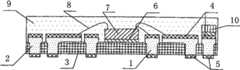
图1为本实用新型无基岛多圈脚静电释放圈无源器件封装结构示意图。Fig. 1 is a schematic diagram of the packaging structure of the passive device of the utility model without a base island and a multi-turn foot electrostatic release ring.
图2为图1的俯视图。FIG. 2 is a top view of FIG. 1 .
图3为以往在金属基板的背面贴上一层耐高温的胶膜图作业。Figure 3 is a picture of pasting a layer of high-temperature-resistant adhesive film on the back of the metal substrate in the past.
图4为以往采用金属基板的正面进行化学蚀刻及表面电镀层作业图。Fig. 4 is a working diagram of chemical etching and surface electroplating on the front side of a metal substrate in the past.
图5为以往形成绝缘脚示意图。FIG. 5 is a schematic diagram of forming insulating pins in the past.
图6为以往形成的掉脚图。Fig. 6 is a diagram of a footfall formed in the past.
图7为以往的封装结构示意图。FIG. 7 is a schematic diagram of a conventional package structure.
图8为图7的俯视图。FIG. 8 is a top view of FIG. 7 .
图中附图标记:Reference signs in the figure:
静电释放圈1、引脚2、无填料的塑封料3、第一金属层4、第二金属层5、不导电粘结物质6、芯片7、金属线8、有填料塑封料9、无源器件10。
(五)具体实施方式(5) Specific implementation methods
参见图1~2,图1为本实用新型无基岛多圈脚静电释放圈无源器件封装结构示意图。图2为图1的俯视图。由图1~2可以看出,本实用新型无基岛多圈脚静电释放圈无源器件封装结构,包括静电释放圈1、引脚2、不导电粘结物质6、芯片7、金属线8和有填料塑封料9,在所述静电释放圈1和引脚2的正面设置有第一金属层4,在所述静电释放圈1和引脚2的背面设置有第二金属层5,所述引脚2设置有多圈,所述引脚2正面延伸到静电释放圈1旁边,在所述引脚2外围的区域、引脚2与静电释放圈1之间的区域、静电释放圈1内外的区域以及引脚2与引脚2之间的区域嵌置有无填料的塑封料3,所述无填料的塑封料3将引脚下部外围、引脚2下部与静电释放圈1下部、所述引脚2正面延伸部分的背面以及引脚2下部与引脚2下部连接成一体,且使所述静电释放圈和引脚背面尺寸小于静电释放圈和引脚正面尺寸,形成上大下小的静电释放圈和引脚结构,在所述静电释放圈1内的无填料塑封料3正面通过不导电粘结物质6设置有芯片7,芯片7正面与引脚2正面第一金属层4之间用金属线8连接,在引脚2与引脚2之间或引脚2与静电释放圈1之间跨接有无源器件10,在所述静电释放圈1和引脚2的上部以及芯片7、金属线8和无源器件10外包封有 填料塑封料9。Referring to Figures 1-2, Figure 1 is a schematic diagram of the packaging structure of the passive device of the utility model without a base island and a multi-turn foot electrostatic discharge ring. FIG. 2 is a top view of FIG. 1 . It can be seen from Figures 1 to 2 that the passive device packaging structure of the utility model has no base island and multi-turn static discharge ring, including
本实用新型可因芯片功能的需要在上述引脚2的正面进行全部区域电镀第一金属层4或是局部区域电镀第一金属层4的制作。In the present invention, the
Claims (1)
Priority Applications (1)
| Application Number | Priority Date | Filing Date | Title |
|---|---|---|---|
| CN2010201826073UCN201681935U (en) | 2010-04-30 | 2010-04-30 | Non-paddle multiturn pin static release ring passive device packaging structure |
Applications Claiming Priority (1)
| Application Number | Priority Date | Filing Date | Title |
|---|---|---|---|
| CN2010201826073UCN201681935U (en) | 2010-04-30 | 2010-04-30 | Non-paddle multiturn pin static release ring passive device packaging structure |
Publications (1)
| Publication Number | Publication Date |
|---|---|
| CN201681935Utrue CN201681935U (en) | 2010-12-22 |
Family
ID=43346971
Family Applications (1)
| Application Number | Title | Priority Date | Filing Date |
|---|---|---|---|
| CN2010201826073UExpired - LifetimeCN201681935U (en) | 2010-04-30 | 2010-04-30 | Non-paddle multiturn pin static release ring passive device packaging structure |
Country Status (1)
| Country | Link |
|---|---|
| CN (1) | CN201681935U (en) |
Cited By (1)
| Publication number | Priority date | Publication date | Assignee | Title |
|---|---|---|---|---|
| WO2013078751A1 (en)* | 2011-11-30 | 2013-06-06 | Jiangsu Changjiang Electronics Technology Co.Ltd | No-exposed-pad ball grid array (bga) packaging structures and method for manufacturing the same |
- 2010
- 2010-04-30CNCN2010201826073Upatent/CN201681935U/ennot_activeExpired - Lifetime
Cited By (1)
| Publication number | Priority date | Publication date | Assignee | Title |
|---|---|---|---|---|
| WO2013078751A1 (en)* | 2011-11-30 | 2013-06-06 | Jiangsu Changjiang Electronics Technology Co.Ltd | No-exposed-pad ball grid array (bga) packaging structures and method for manufacturing the same |
Similar Documents
| Publication | Publication Date | Title |
|---|---|---|
| CN101814482B (en) | Base island lead frame structure and production method thereof | |
| CN101840901A (en) | Lead frame structure of static release ring without paddle and production method thereof | |
| CN201681936U (en) | Passive component packaging structure without substrate | |
| CN201681935U (en) | Non-paddle multiturn pin static release ring passive device packaging structure | |
| CN201681933U (en) | Pin-type packaging structure with direct placement of chip and reactive device | |
| CN201752011U (en) | Foundation island-free and multi-ring pin packaging structure | |
| CN201681877U (en) | Sinking base island exposed encapsulation structure | |
| CN201681903U (en) | Encapsulation structure of base-island exposed and sinking base-island exposed passive device | |
| CN201681893U (en) | Lead frame structure with base islands | |
| CN201681890U (en) | Lead frame structure for direct placement by chip | |
| CN201681891U (en) | Direct-chip-placing multi-turn pin type encapsulation structure | |
| CN201681938U (en) | Non-paddle multiturn pin passive device packaging structure | |
| CN201752007U (en) | Lead frame structure with base island and multiple circles of pins | |
| CN201681872U (en) | Encapsulation structure for multiple base-island exposure type multi-turn pins | |
| CN201681934U (en) | Encapsulating structure for passive device with base island and multi-ring pins | |
| CN201681908U (en) | Insular base exposure and multi-convex-point insular base exposure type multi-circle lead foot passive device packaging structure | |
| CN201681857U (en) | Multi-salient-point base-island exposed single-circle pin packaging structure | |
| CN201681919U (en) | Multi-salient-point base-island exposed and embedded base-island multi-circle pin packaging structure | |
| CN201752012U (en) | Base island exposed and embedded type base island multi-turn pin encapsulation structure | |
| CN201681898U (en) | Base island and sunken base island exposing type encapsulating structure | |
| CN201681911U (en) | Sunken base island exposing and embedding type base island multi-ring pin encapsulating structure | |
| CN201681874U (en) | Insular base exposure type packaging structure | |
| CN201681904U (en) | Base island exposed type and embedded type base island multi-circle pin passive device encapsulating structure | |
| CN201681910U (en) | Sunken base island exposing and embedding type base island passive device encapsulating structure | |
| CN201681915U (en) | Sunk substrate exposure-type and multi-emboss substrate exposure-type multiturn pin packaging structure |
Legal Events
| Date | Code | Title | Description |
|---|---|---|---|
| C14 | Grant of patent or utility model | ||
| GR01 | Patent grant | ||
| CX01 | Expiry of patent term | Granted publication date:20101222 | |
| CX01 | Expiry of patent term |