CN201638995U - Connector - Google Patents
ConnectorDownload PDFInfo
- Publication number
- CN201638995U CN201638995UCN2009203164544UCN200920316454UCN201638995UCN 201638995 UCN201638995 UCN 201638995UCN 2009203164544 UCN2009203164544 UCN 2009203164544UCN 200920316454 UCN200920316454 UCN 200920316454UCN 201638995 UCN201638995 UCN 201638995U
- Authority
- CN
- China
- Prior art keywords
- terminal
- holding
- electronic module
- insulating body
- bottom wall
- Prior art date
- Legal status (The legal status is an assumption and is not a legal conclusion. Google has not performed a legal analysis and makes no representation as to the accuracy of the status listed.)
- Expired - Lifetime
Links
Images


Classifications
- H—ELECTRICITY
- H01—ELECTRIC ELEMENTS
- H01R—ELECTRICALLY-CONDUCTIVE CONNECTIONS; STRUCTURAL ASSOCIATIONS OF A PLURALITY OF MUTUALLY-INSULATED ELECTRICAL CONNECTING ELEMENTS; COUPLING DEVICES; CURRENT COLLECTORS
- H01R12/00—Structural associations of a plurality of mutually-insulated electrical connecting elements, specially adapted for printed circuits, e.g. printed circuit boards [PCB], flat or ribbon cables, or like generally planar structures, e.g. terminal strips, terminal blocks; Coupling devices specially adapted for printed circuits, flat or ribbon cables, or like generally planar structures; Terminals specially adapted for contact with, or insertion into, printed circuits, flat or ribbon cables, or like generally planar structures
- H01R12/70—Coupling devices
- H01R12/71—Coupling devices for rigid printing circuits or like structures
- H01R12/72—Coupling devices for rigid printing circuits or like structures coupling with the edge of the rigid printed circuits or like structures
- H01R12/721—Coupling devices for rigid printing circuits or like structures coupling with the edge of the rigid printed circuits or like structures cooperating directly with the edge of the rigid printed circuits
- H—ELECTRICITY
- H01—ELECTRIC ELEMENTS
- H01R—ELECTRICALLY-CONDUCTIVE CONNECTIONS; STRUCTURAL ASSOCIATIONS OF A PLURALITY OF MUTUALLY-INSULATED ELECTRICAL CONNECTING ELEMENTS; COUPLING DEVICES; CURRENT COLLECTORS
- H01R12/00—Structural associations of a plurality of mutually-insulated electrical connecting elements, specially adapted for printed circuits, e.g. printed circuit boards [PCB], flat or ribbon cables, or like generally planar structures, e.g. terminal strips, terminal blocks; Coupling devices specially adapted for printed circuits, flat or ribbon cables, or like generally planar structures; Terminals specially adapted for contact with, or insertion into, printed circuits, flat or ribbon cables, or like generally planar structures
- H01R12/70—Coupling devices
- H01R12/71—Coupling devices for rigid printing circuits or like structures
- H01R12/72—Coupling devices for rigid printing circuits or like structures coupling with the edge of the rigid printed circuits or like structures
- H01R12/73—Coupling devices for rigid printing circuits or like structures coupling with the edge of the rigid printed circuits or like structures connecting to other rigid printed circuits or like structures
- H01R12/732—Printed circuits being in the same plane
Landscapes
- Coupling Device And Connection With Printed Circuit (AREA)
Abstract
Translated fromChinese
Description
Translated fromChinese【技术领域】【Technical field】
本实用新型有关一种连接器,尤其涉及一种以跨骑方式与电路板两侧相连接的跨骑式连接器。The utility model relates to a connector, in particular to a straddle connector connected to both sides of a circuit board in a straddle manner.
【背景技术】【Background technique】
与本实用新型相关的现有技术请参阅于2004年3月23日公告的美国专利第US6709296号,该项专利揭示了一种连接器,包括有绝缘本体及固持于绝缘本体内的两排导电端子,该两排导电端子分别设有相对设置的接触部及自接触部沿电子模组插入方向延伸出绝缘本体的焊接部,所述焊接部与接触部对应设置为两排。所述两排接触部之间形成用以收容并连接一电子模组的第一收容部,该电子模组上可设置用以传输电源的电源装置;所述两排焊接部之间形成用以收容并连接电路板的第二收容部,从而使焊接部以跨骑方式焊接于电路板的两侧以增大焊接部之间的距离,防止导电端子之间相互干扰;因所述焊接部直接自接触部延伸而成,从而第一收容部与第二收容部沿电子模组插入方向的中心线位于同一直线上,进而安装于第一收容部内的电子模组与安装于第二收容部内的电路板位于同一平面上。Please refer to US Patent No. US6709296 published on March 23, 2004 for the prior art related to the present utility model, which discloses a connector comprising an insulating body and two rows of conductors held in the insulating body Terminals, the two rows of conductive terminals are respectively provided with oppositely arranged contact parts and welding parts extending from the contact parts along the insertion direction of the electronic module to the insulating body, and the welding parts and the contact parts are arranged in two rows correspondingly. Between the two rows of contact parts is formed a first receiving part for accommodating and connecting an electronic module, and the electronic module can be provided with a power supply device for transmitting power; between the two rows of welding parts is formed for Accommodate and connect the second receiving part of the circuit board, so that the welding part is welded on both sides of the circuit board in a straddling manner to increase the distance between the welding parts and prevent mutual interference between the conductive terminals; because the welding part directly Extended from the contact part, so that the center line of the first receiving part and the second receiving part along the electronic module insertion direction are on the same straight line, and then the electronic module installed in the first receiving part and the electronic module installed in the second receiving part The circuit boards are on the same plane.
随着电子产品小型化的发展,电子设备内预留给上述连接器的空间也逐渐减小。然而,由于安装于上述连接器上的电子模组与电路板位于同一直线上,则当位于电子模组一侧的电子装置(如上述电源装置)体积较大时,该电子装置外侧距离电路板的高度或厚度难以降低,且电路板另一侧与电子设备外壳之间的空间未发挥任何作用,从而造成浪费且导致电子设备体积很难缩小,进而无法适应电子产品小型化的发展。With the development of miniaturization of electronic products, the space reserved for the above-mentioned connectors in the electronic equipment is gradually reduced. However, since the electronic module mounted on the above-mentioned connector and the circuit board are located on the same straight line, when the electronic device (such as the above-mentioned power supply device) on the side of the electronic module is relatively large in size, the distance from the outside of the electronic device to the circuit board It is difficult to reduce the height or thickness of the circuit board, and the space between the other side of the circuit board and the housing of the electronic device does not play any role, resulting in waste and making it difficult to reduce the size of the electronic device, which cannot adapt to the development of miniaturization of electronic products.
因此,有必要提供一种具有改良结构的连接器,以克服上述缺陷。Therefore, it is necessary to provide a connector with an improved structure to overcome the above defects.
【实用新型内容】【Content of utility model】
本实用新型的目的在于提供一种偏移设置的连接器以减小组装有本实用新型连接器的电子设备的体积。The purpose of the utility model is to provide a connector arranged offset to reduce the volume of the electronic equipment assembled with the connector of the utility model.
为达上述目的,本实用新型采用如下技术方案:一种连接器,用以连接一电子模组,所述连接器包括绝缘本体及固持于绝缘本体内的若干导电端子,所述绝缘本体设有相对设置的顶壁和底壁、及位于顶壁和底壁之间以插接电子模组的容置槽,所述顶壁和底壁上分别设有用以收容导电端子的固持槽,每一导电端子设有固持于固持槽内的固持部,自固持部延伸入容置槽内的接触部及自固持部延伸出绝缘本体以连接电路板的连接部,所述接触部成两排设置于容置槽的两侧,所述连接部与接触部对应设置为两排并在该两排连接部之间形成收容电路板的收容腔,所述容置槽设有沿电子模组插入方向的中心线,所述收容腔设有与前述中心线平行的中心线,所述容置槽的中心线相对于收容腔的中心线偏移设置。In order to achieve the above purpose, the utility model adopts the following technical solution: a connector for connecting an electronic module, the connector includes an insulating body and a plurality of conductive terminals held in the insulating body, the insulating body is provided with The opposite top wall and bottom wall, and the accommodating groove between the top wall and the bottom wall for inserting the electronic module, the top wall and the bottom wall are respectively provided with holding grooves for accommodating conductive terminals, each The conductive terminal is provided with a holding portion held in the holding groove, a contact portion extending from the holding portion into the accommodating groove, and a connecting portion extending from the holding portion out of the insulating body to connect the circuit board. The contact portions are arranged in two rows on the On both sides of the accommodating groove, the connection part and the contact part are arranged in two rows correspondingly, and a storage cavity for accommodating the circuit board is formed between the two rows of connection parts, and the accommodating groove is provided with a Center line, the storage cavity is provided with a center line parallel to the aforementioned center line, and the center line of the storage tank is offset relative to the center line of the storage cavity.
与现有技术相比,本实用新型具有如下有益效果:本实用新型连接器通过将连接电子模组的容置槽的中心线与连接电路板的收容腔的中心线偏移设置,使得电子模组上设置电源装置时,可设置在电子模组上沿绝缘本体上下方向比电路板低的一侧,此时电源装置顶部沿绝缘本体上下方向至电路板的距离在中心线偏移后得以减小,进而将本实用新型连接器及电子模组安装到电子设备上后,可有效利用电路板两侧的空间,使得电子设备的厚度得以减小,适应电子产品小型化发展的趋势。Compared with the prior art, the utility model has the following beneficial effects: the connector of the utility model offsets the center line of the accommodation groove connected to the electronic module and the center line of the accommodation cavity connected to the circuit board, so that the electronic module When the power supply device is installed on the group, it can be installed on the side of the electronic module that is lower than the circuit board along the up and down direction of the insulating body. Small, and after installing the connector and the electronic module of the utility model on the electronic equipment, the space on both sides of the circuit board can be effectively used, so that the thickness of the electronic equipment can be reduced, adapting to the trend of miniaturization of electronic products.
下面结合附图及较佳实施例对本实用新型作进一步说明。Below in conjunction with accompanying drawing and preferred embodiment the utility model is described further.
【附图说明】【Description of drawings】
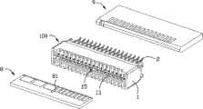
图1为本实用新型连接器及一对接电子模组和电路板的立体图。FIG. 1 is a perspective view of the connector of the present invention and a pair of electronic modules and circuit boards.
图2为图1中电子模组安装于本实用新型连接器上后再安装到电路板上的立体图。Fig. 2 is a perspective view of the electronic module in Fig. 1 installed on the connector of the present invention and then installed on the circuit board.
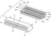
图3为图1中连接器的立体分解图。FIG. 3 is an exploded perspective view of the connector in FIG. 1 .
图4为图1中连接器的另一角度的立体分解图。FIG. 4 is an exploded perspective view of the connector in FIG. 1 from another angle.
图5为本实用新型连接器的剖示示意图。FIG. 5 is a schematic cross-sectional view of the connector of the present invention.
图6为电子模组安装于本实用新型连接器上后再安装到电路板上的剖示示意图。FIG. 6 is a schematic cross-sectional view of the electronic module installed on the connector of the present invention and then installed on the circuit board.
【具体实施方式】【Detailed ways】
请参照图1至图6所示为本实用新型连接器100的较佳实施例,本实用新型连接器100用以与一对接电子模组8电性连接并安装到一电路板9上。所述连接器100包括绝缘本体1及固持于绝缘本体1上的若干导电端子2。所述电子模组8上可设置用以传输电源的电源装置(未图示)以给电路板9上的电子设备提供电源,或其他类似电子装置(未图示)以与电路板9之间传输其他信号。Please refer to FIG. 1 to FIG. 6 , which show a preferred embodiment of the
所述绝缘本体1设有相对设置的顶壁11和底壁12、及位于顶壁11和底壁12之间以插接电子模组8的容置槽13。所述顶壁11设有位于绝缘本体1后端的第一后表面111,所述底壁12设有位于绝缘本体1后端的第二后表面121。所述顶壁11沿电子模组8插入方向延伸的长度小于底壁12沿电子模组8插入方向延伸的长度,从而所述第一后表面111沿电子模组8插入方向位于第二后表面121的前侧并与第二后表面121相平行。所述顶壁11上设有沿电子模组8插入方向贯穿绝缘本体1前后的第一固持槽141以固持导电端子2。所述底壁11上设有沿电子模组8插入方向贯穿绝缘本体1前后的第二固持槽142以固持导电端子2。所述第一固持槽141沿电子模组8插入方向的长度小于第二固持槽142的长度。所述第一固持槽141及第二固持槽142沿绝缘本体1上下方向与容置槽13相贯通,本实用新型中绝缘本体1上下方向与电子模组8插入方向相互垂直。此外,所述绝缘本体1还设有一位于顶壁11和底壁12之间、并将容置槽13分隔成不等长的两部分的挡墙15以防止电子模组8反向插入。所述挡墙15位于容置槽13内并与顶壁11和底壁12垂直设置。所述电子模组8前端设有与该挡墙15相对应设置的凹口81。The insulating housing 1 is provided with a
所述导电端子2包括并排设置于绝缘本体1上的顶壁11内的第一端子21,及与第一端子21相对设置、且并排设置于绝缘本体1的底壁12内的第二端子22,从而使导电端子2成两排平行设置。每一第一端子21设有固持于顶壁11上第一固持槽141内的第一固持部212、自第一固持部212向前延伸的第一接触部211、自第一固持部212末端向上倾斜弯折延伸的第一弯折部214、自第一弯折部214末端向下弯折延伸的第二弯折部215、及自第二弯折部215向下倾斜延伸出绝缘本体1的第一连接部213以连接所述电路板9。所述第一接触部211成一排并排设置、并自第一固持槽141向下延伸入容置槽13内以与电子模组8电性连接。所述第一连接部213与第一接触部211对应设置为一排并焊接在电路板9其中一侧。第一端子21的第一连接部213自第二弯折部215向下弯折以夹持电路板9,从而第二弯折部215与第二端子22沿绝缘本体1上下方向的距离大于第一连接部213与第二端子22之间的距离,以防止电路板9头部与第一端子21后侧干涉而造成第一连接部213与电路板9连接不稳定。此外,所述第一接触部211与第一连接部213沿绝缘本体1上下方向位于第一固持部212的两侧,其中第一接触部211位于第一固持部212的下侧,而第一连接部213位于第一固持部212的上侧。The
每一第二端子22设有固持于底壁12上第二固持槽142内的第二固持部222、自第二固持部222向前延伸的第二接触部221、自第二固持部222末端向上弯折延伸的第三弯折部224、及自第三弯折部224末端向上并向后延伸出绝缘本体1的第二连接部223以连接所述电路板9。所述第二接触部221成一排与第一接触部211相对设置,且所述第二接触部221自第二固持槽142向上延伸入容置槽13内以与第一接触部211共同将电子模组8夹持于容置槽13内。所述第二连接部223与第二接触部221对应设置为一排并焊接在电路板9的另一侧,从而使导电端子2的连接部213、223之间的距离拉大,防止导电端子2之间相互干扰。所述第二接触部221与第二连接部223沿绝缘本体1上下方向均位于第二固持部222的上侧,且第二连接部223位于第二接触部221的上侧。此外,所述第一弯折部214、第三弯折部224及第二弯折部215沿电子模组8插入方向错开设置,且第三弯折部224位于第一弯折部214与第二弯折部215之间。所述第二固持部222沿电子模组8插入方向的长度大于第一固持部212的长度。Each
由以上可得,本实用新型连接器100中第一接触部211与第二接触部221可将电子模组8夹持在容置槽13内,而第一连接部213与第二连接部223相对设置并在两者之间形成收容腔16用以将电路板9夹持在收容腔16内。又由以上导电端子2结构可得,本实用新型中用以收容电子模组8的容置槽13设有沿电子模组8插入方向的中心线L1,所述收容腔16设有与中心线L1平行中心线L2,所述中心线L1相对于中心线L2沿绝缘本体1上下方向偏移设置,且中心线L1位于中心线L2的下方,从而电子模组8上的电源装置可设置在电子模组8的上方位置,此时电源装置顶部沿绝缘本体1上下方向至电路板9顶面的距离在中心线L1向下偏移后得以减小,进而将本实用新型连接器100及电子模组8安装到电子设备上后,可有效利用电路板9两侧的空间,使得电子设备的厚度得以减小,适应电子产品小型化发展的趋势。此外,所述第一后表面111沿电子模组8插入方向位于第二后表面121的前侧,从而在将本实用新型连接器100向电路板9上安装时,第二后表面121可与电路板9相抵持,以防止本实用新型连接器100过度安装时,电路板9前端将第一端子21后侧向上抵顶而导致第一连接部213与电路板9接触不良。From the above, it can be concluded that the
综上所述,以上仅为本实用新型的较佳实施例而已,不应以此限制本实用新型的范围,即凡是依本实用新型权利要求书及实用新型说明书内容所作的简单的等效变化与修饰,皆应仍属本实用新型专利涵盖的范围内。In summary, the above are only preferred embodiments of the utility model, and should not limit the scope of the utility model, that is, any simple equivalent changes made according to the claims of the utility model and the content of the utility model description All should still belong to the scope that the utility model patent covers.
Claims (10)
Translated fromChinesePriority Applications (2)
| Application Number | Priority Date | Filing Date | Title |
|---|---|---|---|
| CN2009203164544UCN201638995U (en) | 2009-12-03 | 2009-12-03 | Connector |
| US12/862,957US8075343B2 (en) | 2009-12-03 | 2010-08-25 | Straddle card edge connector |
Applications Claiming Priority (1)
| Application Number | Priority Date | Filing Date | Title |
|---|---|---|---|
| CN2009203164544UCN201638995U (en) | 2009-12-03 | 2009-12-03 | Connector |
Publications (1)
| Publication Number | Publication Date |
|---|---|
| CN201638995Utrue CN201638995U (en) | 2010-11-17 |
Family
ID=43083500
Family Applications (1)
| Application Number | Title | Priority Date | Filing Date |
|---|---|---|---|
| CN2009203164544UExpired - LifetimeCN201638995U (en) | 2009-12-03 | 2009-12-03 | Connector |
Country Status (2)
| Country | Link |
|---|---|
| US (1) | US8075343B2 (en) |
| CN (1) | CN201638995U (en) |
Cited By (2)
| Publication number | Priority date | Publication date | Assignee | Title |
|---|---|---|---|---|
| CN109196733A (en)* | 2016-05-16 | 2019-01-11 | 3M创新有限公司 | Electric connector for printed circuit board |
| CN112290262A (en)* | 2015-09-08 | 2021-01-29 | 安费诺富加宜(亚洲)私人有限公司 | Power connector |
Families Citing this family (26)
| Publication number | Priority date | Publication date | Assignee | Title |
|---|---|---|---|---|
| TWI411175B (en)* | 2010-10-05 | 2013-10-01 | Advanced Connectek Inc | Improved high speed backplane connector |
| TWI449273B (en)* | 2011-05-04 | 2014-08-11 | Hon Hai Prec Ind Co Ltd | Electrical connector and assembly method |
| CN102801006B (en) | 2011-05-23 | 2014-08-27 | 富士康(昆山)电脑接插件有限公司 | Electric connector |
| US8684757B2 (en)* | 2012-04-27 | 2014-04-01 | International Business Machines Corporation | Memory module connector with air deflection system |
| US9716327B2 (en)* | 2012-09-28 | 2017-07-25 | Intel Corporation | System, circuit module, and circuit module connector |
| CN203135017U (en)* | 2013-01-09 | 2013-08-14 | 富士康(昆山)电脑接插件有限公司 | Card edge connector |
| JP6237368B2 (en)* | 2014-03-18 | 2017-11-29 | 日立金属株式会社 | Communication module and connector for communication module |
| WO2016196641A1 (en)* | 2015-06-01 | 2016-12-08 | Molex, Llc | Connector with dual card slots |
| JP6523802B2 (en)* | 2015-06-09 | 2019-06-05 | 山一電機株式会社 | Transceiver module plug connector |
| CN108701922B (en) | 2015-07-07 | 2020-02-14 | Afci亚洲私人有限公司 | Electrical connector |
| JP6448505B2 (en)* | 2015-10-02 | 2019-01-09 | モレックス エルエルシー | Card edge connector |
| FR3054081B1 (en)* | 2016-07-13 | 2022-07-15 | Zodiac Aero Electric | DEVICE FOR THE ELECTRICAL CONNECTION OF POWER DISTRIBUTION PLATES AND ELECTRIC POWER DISTRIBUTION SYSTEM PROVIDED WITH SUCH A CONNECTION DEVICE |
| US20180034211A1 (en)* | 2016-07-26 | 2018-02-01 | Foxconn Interconnect Technology Limited | Electrical connector assembly |
| CN114512840B (en) | 2017-10-30 | 2024-06-25 | 安费诺富加宜(亚洲)私人有限公司 | Low crosstalk card edge connector |
| JP6981859B2 (en)* | 2017-11-28 | 2021-12-17 | タイコエレクトロニクスジャパン合同会社 | connector |
| JP7298998B2 (en)* | 2018-07-17 | 2023-06-27 | タイコエレクトロニクスジャパン合同会社 | connector |
| CN113169484A (en) | 2018-10-09 | 2021-07-23 | 安费诺商用电子产品(成都)有限公司 | High density edge connector |
| TWI693758B (en)* | 2018-12-03 | 2020-05-11 | 宣德科技股份有限公司 | High frequency connector |
| TWM582251U (en) | 2019-04-22 | 2019-08-11 | 香港商安費諾(東亞)有限公司 | Connector set with hidden locking mechanism and socket connector thereof |
| US11973286B2 (en) | 2020-06-01 | 2024-04-30 | Amphenol Commercial Products (Chengdu) Co., Ltd. | Electrical connector and manufacturing method thereof |
| CN212874843U (en)* | 2020-08-31 | 2021-04-02 | 安费诺商用电子产品(成都)有限公司 | Electrical connector |
| CN114597707A (en) | 2020-12-04 | 2022-06-07 | 安费诺商用电子产品(成都)有限公司 | Card edge connector with locking system |
| CN216488833U (en) | 2021-10-27 | 2022-05-10 | 安费诺商用电子产品(成都)有限公司 | electrical connector |
| CN217215360U (en)* | 2021-12-27 | 2022-08-16 | 安费诺商用电子产品(成都)有限公司 | Card edge connector |
| US11811157B2 (en)* | 2022-03-03 | 2023-11-07 | Dell Products L.P. | Printed circuit board edge connector |
| DE102023123975A1 (en)* | 2023-09-06 | 2025-03-06 | Valeo Schalter Und Sensoren Gmbh | Printed circuit board unit for an electronic device with at least two printed circuit boards which are at least electrically connected to one another by at least one connector, printed circuit board, electronic device and vehicle |
Family Cites Families (12)
| Publication number | Priority date | Publication date | Assignee | Title |
|---|---|---|---|---|
| US3365696A (en)* | 1965-08-30 | 1968-01-23 | Rogers Corp | Simplified connector for male type terminations |
| US3482201A (en)* | 1967-08-29 | 1969-12-02 | Thomas & Betts Corp | Controlled impedance connector |
| JPS6243479U (en)* | 1985-09-02 | 1987-03-16 | ||
| US5160275A (en)* | 1990-09-06 | 1992-11-03 | Hirose Electric Co., Ltd. | Electrical connector for circuit boards |
| US5295852A (en)* | 1993-07-12 | 1994-03-22 | The Whitaker Corporation | Coplanar computer docking system |
| US5531615A (en)* | 1993-08-05 | 1996-07-02 | The Whitaker Corporation | Coplanar computer docking apparatus |
| JP3485555B2 (en) | 1999-11-26 | 2004-01-13 | 株式会社アドバンテスト | connector |
| JP4781237B2 (en)* | 2006-11-15 | 2011-09-28 | モレックス インコーポレイテド | Edge connector |
| US7416452B1 (en)* | 2007-03-15 | 2008-08-26 | Hon Hai Precision Ind. Co., Ltd. | Electrical connector |
| CN201117866Y (en)* | 2007-10-19 | 2008-09-17 | 富士康(昆山)电脑接插件有限公司 | card edge connector |
| JP4753055B2 (en)* | 2008-05-21 | 2011-08-17 | Smc株式会社 | Stacking connector |
| US8282402B2 (en)* | 2009-12-23 | 2012-10-09 | Fci Americas Technology Llc | Card-edge connector |
- 2009
- 2009-12-03CNCN2009203164544Upatent/CN201638995U/ennot_activeExpired - Lifetime
- 2010
- 2010-08-25USUS12/862,957patent/US8075343B2/enactiveActive
Cited By (4)
| Publication number | Priority date | Publication date | Assignee | Title |
|---|---|---|---|---|
| CN112290262A (en)* | 2015-09-08 | 2021-01-29 | 安费诺富加宜(亚洲)私人有限公司 | Power connector |
| US11621511B2 (en) | 2015-09-08 | 2023-04-04 | Fci Usa Llc | Electrical power connector configured for high current density |
| CN109196733A (en)* | 2016-05-16 | 2019-01-11 | 3M创新有限公司 | Electric connector for printed circuit board |
| CN109196733B (en)* | 2016-05-16 | 2020-11-03 | 3M创新有限公司 | Electrical connector for printed circuit board |
Also Published As
| Publication number | Publication date |
|---|---|
| US8075343B2 (en) | 2011-12-13 |
| US20110136388A1 (en) | 2011-06-09 |
Similar Documents
| Publication | Publication Date | Title |
|---|---|---|
| CN201638995U (en) | Connector | |
| US10205256B2 (en) | Plug and electrical connector component | |
| CN201204309Y (en) | electrical connector | |
| CN102354882B (en) | Electrical connector | |
| CN201230069Y (en) | Electric connector | |
| CN201323275Y (en) | Electric connector | |
| CN201397973Y (en) | Electric connector | |
| CN102377053B (en) | Electric connector | |
| CN201285822Y (en) | Electric connector | |
| CN201639018U (en) | Electric connector | |
| CN201285890Y (en) | Electric connector | |
| CN101728663A (en) | Cable connector assembly | |
| CN101771226A (en) | electrical connector | |
| CN102832479A (en) | Electrical connector | |
| CN102882039B (en) | Electric connector | |
| CN201252186Y (en) | Card edge connector | |
| CN204696369U (en) | Electric connector | |
| CN201130742Y (en) | Electrical connectors and electrical connector combinations | |
| CN201178149Y (en) | electrical connector | |
| CN202363647U (en) | Card edge connector assembly | |
| CN201639020U (en) | Electric connector | |
| CN202004177U (en) | Electric connector | |
| CN202004179U (en) | Electric connector | |
| CN101740926B (en) | Electric connector | |
| CN202076488U (en) | Electric connector |
Legal Events
| Date | Code | Title | Description |
|---|---|---|---|
| C14 | Grant of patent or utility model | ||
| GR01 | Patent grant | ||
| CX01 | Expiry of patent term | ||
| CX01 | Expiry of patent term | Granted publication date:20101117 |